Optically and Electrically Tunable Dirac Points and Zitterbewegung in Graphene-Based Photonic Superlattices
Abstract
We demonstrate that graphene-based photonic superlattices provide a versatile platform for electrical and all-optical control of photonic beams with deep-subwavelength accuracy. Specifically, by inserting graphene sheets into periodic metallo-dielectric structures one can design optical superlattices that posses photonic Dirac points (DPs) at frequencies at which the spatial average of the permittivity of the superlattice, , vanishes. Similar to the well-known zero- bandgaps, we show that these zero- DPs are highly robust against structural disorder. We also show that, by tuning the graphene permittivity via the optical Kerr effect or electrical doping, one can induce a spectral variation of the DP exceeding , at mid-IR and THz frequencies. The implications of this wide tunability for the photonic Zitterbewegung effect in a vicinity of the DP are explored too.
pacs:
Valid PACS appear hereIntroduction. One of the most daunting challenges one has to overcome in order to develop ultra-fast active photonic nanodevices is the extremely narrow tunability of physical parameters of optical media. For example, while the conductivity of semiconductors can be varied by orders of magnitude with the help of impurity doping or thermally, the index of refraction of optical media, which is the main parameter defining their optical properties, can hardly be tuned by more than . Several approaches that address this key problem have been proposed, including the resort to plasmonic materials whose optical nonlinearity is enhanced by strong optical fields associated with the resonant excitation of surface-plasmon polaritons (SPPs) szg02prl ; cvb11s ; po04prl , the use of strongly anisotropic materials whose optical response can be controlled via the polarization of the excitation field esz04ol ; obt13prl , reconfigurable metamaterials pak10nl , embedding liquid crystals into a photonic-crystal matrix wkk07oe , and tuning the material refractive index via carrier injection cpz06n . While promising if targeted at specific applications, the efficiency of these methods is generally limited by high-power requirements, slow optical response, and reduced spectral tunability.
A recently introduced photonic platform that contains all the ingredients needed to achieve ultra-fast broad optical tunability at the nanoscale is graphene Bonaccorso ; Chen ; Fei . Compared to the SPPs in metals, graphene plasmons are localized within much smaller regions, provide a much larger optical near-field enhancement, and can pass significantly longer distances Jablan ; Koppens . Equally important, the conductivity of graphene and, implicitly, its electrical permittivity can be varied substantially, locally and ultra-fast, by means of chemical doping or gate voltage Yan ; YanBis ; Yao ; Fang . For example, changing the Fermi level by a mere causes the relative variation of the real part of the permittivity, at the wavelength, by . Depositing graphene onto the surface of specific materials, which may be both dielectrics and metals, a variety of graphene-based layered nanostructures have been designed, and their implementations in functional devices have been demonstrated Yan . The most salient feature of these photonic superlattices is that, by incorporating graphene into their periodic structure, the band-structure and thus their optical response can be dynamically tuned. This key property, in conjunction with relatively low loss and extremely tight confinement of the graphene plasmons, opens up promising applications of tunable graphene photonic superlattices (GPSs) at mid-IR and at THz wavelengths. In addition to these important practical considerations, GPSs can also play a major role at the fundamental level. Specifically, it has been suggested that electron-wave dynamics in graphene heterojunctions are in many ways similar to the propagation of optical beams in photonic superlattices containing positive- and negative-index materials Bliokh , intriguing phenomena such as the Klein tunneling Shytov ; Young and Zitterbewegung (ZB) effect 2DZB ; 1DZB1 ; Nam ; 1DZB2 ; Liang ; 1DZB3 being observed in both physical systems.
In this Rapid Communication we demonstrate that, by including graphene sheets into the unit cell of metallo-dielectric superlattices, one can readily design GPSs that posses electrically and optically tunable Dirac points (DPs) and feature the ZB of optical beams propagating near the DPs. A remarkable property of these DPs is that they form when the spatial average of the permittivity of the superlattice vanishes, , an immediate consequence of this fact being their remarkable robustness against structural disorder. To add specificity to these ideas, we consider, as an example of a GPS, the one-dimensional (1D) periodic structure depicted in Fig. 1(a). It has a three-layer unit cell, graphene-metal-dielectric, the metallic and dielectric layers chosen in this work being silver and silicon, respectively. The dispersion relation of the structure is easily found by using the transfer-matrix method (see Supplemental Material SuplMat for the derivation of this relation), and is given by
| (1) |
where is the Bloch wave vector, the propagation wave vector, , , and are the thickness of the layers, is the period of the supercell, , and , with , where , , and stand for graphene, silicon, and silver, respectively. For convenience, we here define , , and . By fixing frequency in Eq. (1), dependence determines the spatial dispersion relation for the particular frequency.
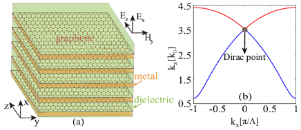
Tunability and robustness of the Dirac points. A peculiar property of the band structure of such GPSs is that, if it possesses two transmission bands, then the bands intersect at the center of the Brillouin zone, , giving rise to the photonic DP [see Fig. 1(b)]. For such a two-band configuration to occur, the thickness of the dielectric and metallic layers should be larger than certain critical values. As mentioned above, a DP in our photonic structure exists provided that the real part of the average permittivity of the superlattice vanishes, namely,
| (2) |
DPs are well known in solid-state physics, being at the origin of many remarkable properties of recently discovered materials, such as graphene and topological insulators. In this case they are singular points in the electron energy-band structure, and the aforementioned similarities between electron and photon wave dynamics suggest that DPs can exist too in the photonic band structure of certain periodic structures, one such example being the GPS presented in Fig. 1(a). As we demonstrate in this study, the graphene component of the present photonic superlattice allows one to tune the wavelength of the photonic DPs by simply varying the chemical potential of graphene, . More specifically, changing by external means (e.g., gate voltage, chemical doping, etc.), one varies the permittivity of graphene and therefore one can tune the wavelength, , at which condition holds. These ideas are illustrated in Fig. 2(a), where we plot the dependence of the wavelength of the DP on . Note that a spectral shift of more than can be achieved changing by . The variation of the corresponding band structure is presented in Fig. 2(b).
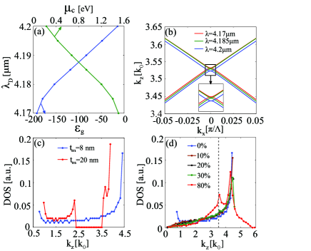
Similar to zero- band-gaps, which are formed when the spatial average of the refractive index of a Bragg grating vanishes, DPs in our photonic structure are particularly robust against disorder added to the system. This behavior is expected because structural disorder weakly affects the spatial average of the permittivity, hence its vanishing, which determines the existence of DPs, persists in the presence of disorder as well. To illustrate this phenomenon, we present in Figs. 2(c) and 2(d) the density of states (DOS) of periodic and disordered GPSs, respectively. In the calculations, we used two superlattices, one selected so as to possess a DP (at ), whereas the other one is a regular superlattice featuring a Bragg gap, at . The DOS of these two superlattices is extracted from , see the results in Fig. 2(c). As expected, while the DOS for the superlattice featuring a Bragg gap exhibits a conspicuous wide region of forbidden states (), the superlattice possessing a DP shows nonvanishing DOS in the whole spectrum. The robustness of the DP against the structural disorder is confirmed in Fig. 2(d), where we display DOS for the disordered superlattice at several different levels of the disorder. It is introduced by assuming random fluctuations of the metallic-layer thickness around its average value, namely, the -th thickness is , where is the average thickness (we choose here), and is a random perturbation. We assume to be uniformly distributed in the interval of , hence the disorder level may be characterized by . The DOSs in Fig. 2(d) clearly demonstrates that, even when the disorder level is increased to , the DP is preserved, appearing as a spectral peak in the DOS, at .
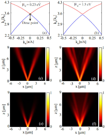
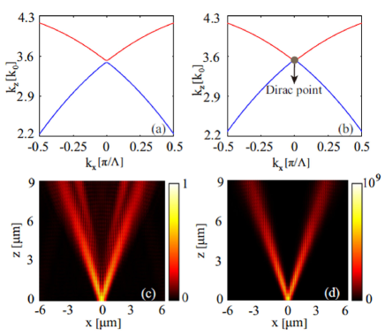
Real-time tunability of the band-structure of the GPS provides an effective way to control the excitation and propagation of optical beams. Figures 3(a) and 3(b) show that, when one varies from to , the band structure transforms from a gapless one, which possesses a DP, to a gapped structure, this effect being accompanied by a dramatic change in the beam-propagation dynamics. At the DP, a normally incident Gaussian beam splits into two, as the upper- and lower-band excitations are not resolved, due to the fact that the two bands have identical slopes near the DP [see Fig. 3(c)]. By contrast, when a gap opens the output pattern exhibits four beams, due to the difference in the slopes of the upper and lower bands near [as per Fig. 3(d)]. Taking losses in graphene and metallic layers into account yields similar patterns of the output optical field [Figs. 3(e) and 3(f)]; however, as expected, the output beams now decay in the course of the propagation. In Figs. 3(e) and 3(f) we used the scattering time, , which was measured in an ionic-liquid gating configuration Ph , the achieved Fermi level being as large as Ye ; Efe .
Optically tunable Dirac points. In addition to electrical means, the wavelength at the DPs can be tuned by means of the intrinsic optical nonlinearity of graphene, or of the dielectric and metallic layers as well. Such nonlinearity-induced tunability of the DP is possible in our superlattices because, as explained above, the DPs form when the real part of the average permittivity is zero. Thus, nonlinear optical effects that change the refractive index can be used to tune the permittivity in or out of the zero-average state, thus providing all-optical means to control the formation of DPs. The optical nonlinearity of graphene is expected to be particularly strong, due to its unusually large third-order nonlinear susceptibility Hendry , as well as the tightly localized optical field supported by graphene sheets.
Figure 4 illustrates the creation/destruction of a DP under the action of the optical Kerr effect, induced in graphene and the neighboring silicon layer. At low optical powers, starting with a superlattice for which , the two transmission bands are separated by a gap, as seen in Fig. 4(a). When the input power increases, both graphene and silicon are affected by the Kerr nonlinearity, their permittivities varying by and , respectively. As a result, the average permittivity of the structure, , gradually increases and the corresponding band structure is modified as well. At some particular value of the optical power, becomes equal to zero, so that, as shown in Fig. 4(b), the photonic gap closes and a DP re-emerges. For the particular case illustrated in Fig. 4, and . The propagation of a TM-polarized Gaussian beam, both in the linear and nonlinear regimes, is presented in Figs. 4(c) and 4(d), respectively. One can see that, when the power of the input beam increases, the beam dynamics changes from the typical discrete diffraction to 1D conical diffraction, which is a manifestation of the formation of the DP in the latter case.
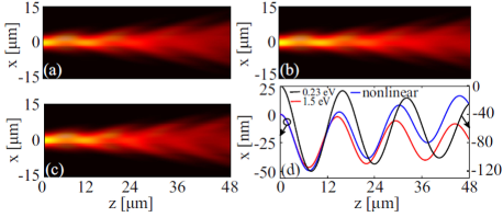
Tunable Zitterbewegung effect. Finally, we point out that the control of the DP and band-structure of GPSs suggest a convenient way to implement, in the classical-optics context, a series of intriguing quantum-mechanical phenomena. As a relevant example, here we consider the ZB effect, which, in the relativistic quantum mechanics, refers to rapid oscillations (trembling) of a moving electron around its average position. The ZB of electrons arises because of the interference of particle and antiparticle components of the wave function. The electron ZB oscillations having extremely high frequencies, of about , therefore this phenomenon is not accessible to experimental observations. Recently, optical analogs of the ZB were studied in 1D 1DZB1 ; Nam ; 1DZB2 ; Liang ; 1DZB3 and 2D 2DZB photonic crystals. Here we demonstrate that GPSs are highly suitable physical systems to study this effect. To this end, we show in Figs. 5(a) and 5(b) the beam propagation at two different values of the chemical potential, and , respectively. Note that in both cases the GPS has gaps in the wave-vector space, the gap at being wider. In the latter case, the ZB has a smaller oscillation amplitude and a larger frequency, which is consistent with the findings reported in Ref. 1DZB2 . This behavior is more clearly observed in Fig. 5(d), where we plot the evolution of the beam center, .
Still more important, GPSs provide a reliable platform to implement “nonlinear quantum mechanics”, as shown in Fig. 5(c), where we examine the ZB dynamics affected by the self-focusing nonlinearity, associated with the graphene and silicon layers. The figure shows that, while the ZB amplitude and frequency remain almost unaltered, the self-focusing nonlinearity leads to a spatial walk-off of the ZB, viz., monotonic spatial drift of the beam’s center in one direction, in the course of its propagation. Note that, as the thickness of the layers of the GPSs can be scaled so that the real part of its averaged permittivity remains equal to zero, one can easily extend the ZB effect, and the emulation of other DP-related quantum phenomena, into the THz and other spectral ranges, different from the standard optical one.
Conclusion. We have proposed graphene-based photonic superlattices which should provide a highly effective and robust approach for the control of photonic beams at the nanoscale. By taking advantage of the strong dependence of the graphene permittivity on the chemical potential, it is demonstrated that, due to the peculiar topology of their photonic band structure, specially designed photonic superlattices, incorporating graphene sheets interlaid with metallic and dielectric layers, feature large electrical and optical tunability. Implications of our findings to applications and studies of fundamental effects, such as Zitterbewegung, are proposed too.
Acknowledgments. The work of H. Deng and F. Ye was supported by Innovation Program of Shanghai Municipal Education Commission (Grant No. 13ZZ022) and the National Natural Science Foundation of China (Grant No. 11104181 and 61475101). The work of N.C.P. was supported by the Engineering and Physical Sciences Research Council, grant No EP/J018473/1. This author acknowledges the hospitality of the Department of Physics and Astronomy of Shanghai Jiao Tong University during a visit to which this paper was written. B.A.M. appreciates a partial support through Grant No. B12024 from “Program of introducing talents of discipline to universities” (China).
References
- (1) I. I. Smolyaninov, A. V. Zayats, A. Gungor, and C. C. Davis, Phys. Rev. Lett. 88, 187402 (2002).
- (2) W. Cai, A. P. Vasudev, and M. L. Brongersma, Science 333, 1720 (2011).
- (3) N. C. Panoiu and R. M. Osgood, Nano Lett. 4, 2427 (2004).
- (4) J. Elliott, I. I. Smolyaninov, N. I. Zheludev, and A. V. Zayats, Opt. Lett. 29, 1414 (2004).
- (5) E. J. Osley, C. G. Biris, P. G. Thompson, R. R. F. Jahromi, P. A. Warburton, and N. C. Panoiu, Phys. Rev. Lett. 110, 087402 (2013).
- (6) I. M. Pryce, K. Aydin, Y. A. Kelaita, R. M. Briggs, and H. A. Atwater, Nano Lett. 10, 4222 (2010).
- (7) D. H. Werner, D.-H. Kwon, I.-C. Khoo, I.-C. Kildishev, A. V. Shalaev, and M. Vladimir, Opt. Express 15, 3342 (2007).
- (8) H.-T. Chen, W. J. Padilla, J. M. O. Zide, A. C. Gossard, A. J. Taylor, and R. D. Averitt, Nature (London)444, 597 (2006).
- (9) F. Bonaccorso, Z. Sun, T. Hasan, and A. C. Ferrari, Nat. Photon. 4, 611 (2010).
- (10) J. Chen, M. Badioli, P. A. Gonzalez, S. Thongrattanasiri, F. Huth, J. Osmond, M. Spasenovic, A. Centeno, A. Pesquera, P. Godignon, A. Z. Elorza, N. Camara, F. J. G. de Abajo, R. Hillenbrand, and F. H. L. Koppens, Nature (London)487, 77 (2012).
- (11) Z. Fei, A. S. Rodin, G. O. Andreev, W. Bao, A. S. McLeod, M. Wagner, L. M. Zhang, Z. Zhao, M. Thiemens, G. Dominguez, M. M. Fogler, A. H. Castro Neto, C. N. Lau, F. Keilmann, and D. N. Basov, Nature (London)487, 82 (2012).
- (12) M. Jablan, H.Buljan, and M. Soljacic, Phys. Rev. B 80, 245435 (2009).
- (13) F. H. L. Koppens, D. E. Chang, and F. J. G. de Abajo, Nano Lett. 11, 3370 (2011).
- (14) H. Yan, X. Li, B. Chandra, G. Tulevski, Y. Wu, M. Freitag, W. Zhu, P. Avouris, F. Xia, Nat. Nanotechnol. 7, 330 (2012).
- (15) H. Yan, F. Xia, Z. Li, and P. Avouris, New J. Phys. 14, 125001 (2012).
- (16) Y. Yao, M. A. Kats, P. Genevet, N. Yu, Y. Song, J. Kong, and F. Capasso, Nano Lett. 13, 1257 (2013).
- (17) Z. Fang, Y. Wang, A. E. Schlather, Z. Liu, P. M. Ajayan, F. J. G. de Abajo, P. Nordlander, X. Zhu, and N. J. Halas, Nano Lett. 14, 299 (2014).
- (18) Y. P. Bliokh, V. Freilikher, and F. Nori, Phys. Rev. B 87, 245134 (2013).
- (19) A. V. Shytov, M. S. Rudner, and L. S. Levitov, Phys. Rev. Lett. 101, 156804 (2008).
- (20) A. F. Young and P. Kim, Nat. Phys. 5, 222 (2009).
- (21) X. Zhang, Phys. Rev. Lett. 100, 113903 (2008).
- (22) S. Longhi, Opt. Lett. 35, 235 (2010).
- (23) S. H. Nam, A. J. Taylor, and A. Efimov, Opt. Express 18, 10120 (2010).
- (24) F. Dreisow, M. Heinrich, R. Keil, A. Tunnermann, S. Nolte, S. Longhi, and A. Szameit, Phys. Rev. Lett. 105, 143902 (2010).
- (25) Q. Liang, Y. Yan, and J. Dong, Opt. Lett. 36, 2513 (2011).
- (26) S. Ding and G. Wang, Opt. Lett. 31, 603 (2014).
- (27) See Supplemental Material at [URL will be inserted by publisher] for 1) description of the physical models of permittivity of noble metals and graphene; 2) derivation of the dispersion relation of the Bloch modes of graphene superlattices; 3) a discussion of the influence of metallic and graphene optical losses on the Zitterbewegung effect; and 4) a discusssion of the effective linear and nonlinear susceptibilities of graphene.
- (28) P. Tassin, T. Koschny, and C. M. Soukoulis, Science 341, 620 (2013).
- (29) J. Ye, M. F. Craciun, M. Koshino, S. Russo, S. Inoue, H. Yuan, H. Shimotani, A. F. Morpurgo, and Y. Iwasa, Proc. Natl. Acad. Sci. 108, 13002 (2011).
- (30) D. K. Efetov and P. Kim, Phys. Rev. Lett. 105, 256805 (2010).
- (31) E. Hendry, P. Hale, J. Moger, A. Savchenko, and S. Mikhailov, Phys. Rev. Lett. 105, 097401 (2010).