Enhanced thermionic-dominated photoresponse in graphene Schottky junctions
Abstract
Vertical heterostructures of van der Waals materials enable new pathways to tune charge and energy transport characteristics in nanoscale systems. We propose that graphene Schottky junctions can host a special kind of photoresponse which is characterized by strongly coupled heat and charge flows that run vertically out of the graphene plane. This regime can be accessed when vertical energy transport mediated by thermionic emission of hot carriers overwhelms electron-lattice cooling as well as lateral diffusive energy transport. As such, the power pumped into the system is efficiently extracted across the entire graphene active area via thermionic emission of hot carriers into a semiconductor material. Experimental signatures of this regime include a large and tunable internal responsivity with a non-monotonic temperature dependence. In particular, peaks at electronic temperatures on the order of the Schottky potential and has a large upper limit ( when ). Our proposal opens up new approaches for engineering the photoresponse in optically-active graphene heterostructures.
pacs:
Vertical heterostructures comprising layers of van der Waals (vdW) materials have recently emerged as a platform for designer electronic interfaces geimvdw . Of special interest are heterostructures which feature tunable interlayer transport characteristics, as exemplified by g/X Schottky junctions gschottky2 ; gschottky1 ; gschottky3 ; gsolar ; gsolar2 ; britnellscience ; ws2heterostructures ; heterostructures ; britnellnanolett ; here ‘g’ denotes graphene, and X is a semiconductor material, such as Si, MoS2 or WSe2. These junctions are characterized by Schottky barriers that span two orders of magnitude and exhibit in situ control through applied bias or by using gate potentials ws2heterostructures ; gschottky2 ; gschottky1 ; britnellscience ; schottkyreport . The wide range of achievable across the g/X interface, combined with the unique graphene photoresponse mediated by long-lived hot carriers (elevated electronic temperatures, , different from those of the lattice, macdonald ; wong ; gabor ; song ; graham ; betz ), make graphene Schottky junctions a prime target for accessing novel vertical energy transport regimes koppens .
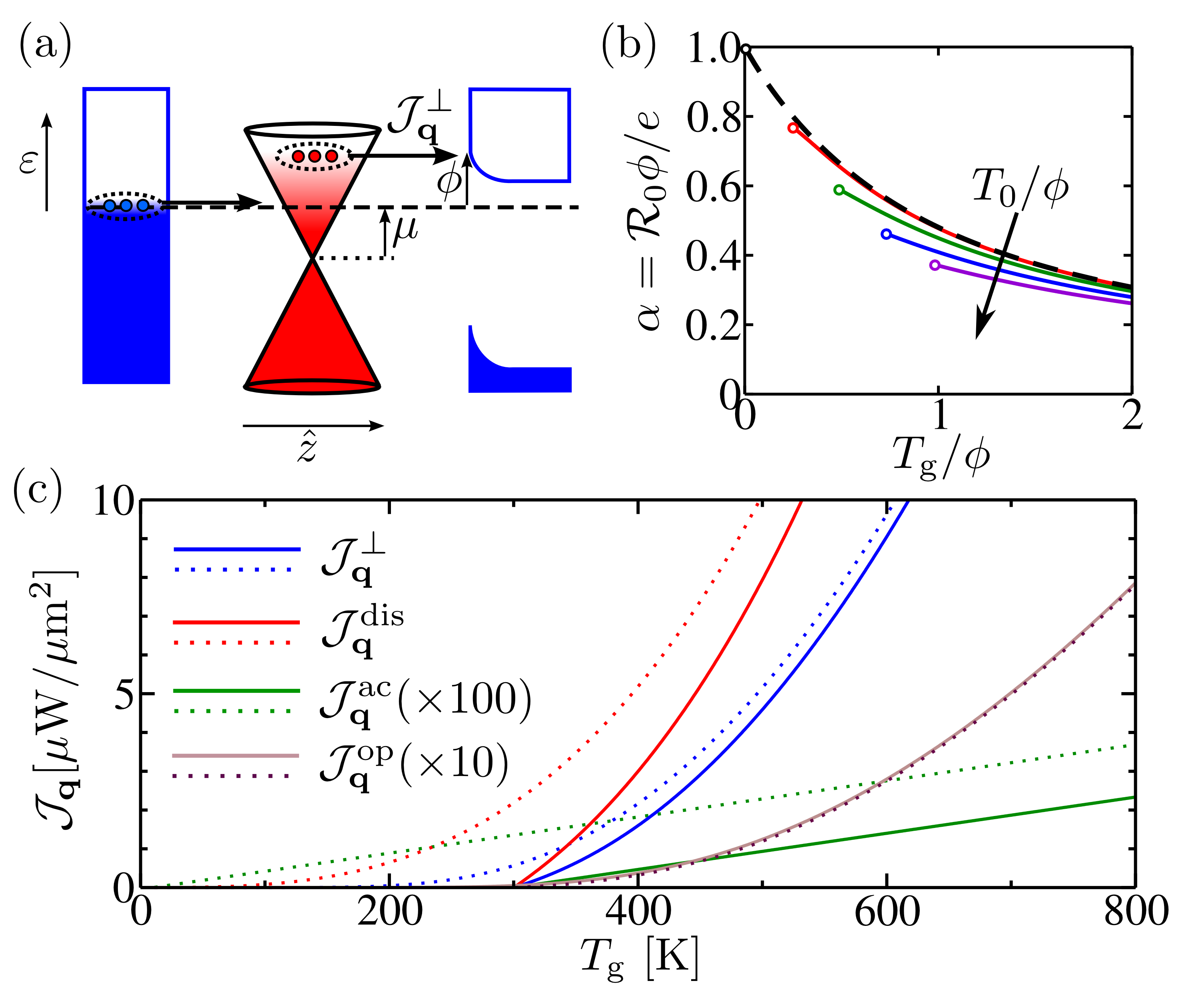
Here we show that specially designed graphene Schottky junctions can host an enhanced thermionic-dominated photoresponse driven by strongly coupled charge and energy currents. Such photoresponse proceeds, as illustrated in Fig. 1a, via the thermionic emission of graphene hot carriers with energy larger than the Schottky barrier. At steady state, an equal number of cold carriers are injected at the Fermi surface through an ohmic contact, giving a net flow of heat out of the graphene electronic system balancing the energy pumped into the system.
Strikingly, thermionic emission yields strong heat transport running vertically out of the hot electron system, which dominates over more conventional electronic cooling channels, e.g. electron-lattice cooling. Indeed, we find that can be significant in graphene (see Fig. 1c) when , dominating over acoustic and optical phonon cooling macdonald ; wong in pristine graphene Schottky junctions; also overwhelms in-plane (lateral) diffusive energy transport. We find that the values of are competitive with disorder-assisted cooling song ; graham ; betz in more dirty devices.
Graphene is essential to our proposal due to a unique combination of electronic characteristics. First, fast intraband Auger-type scattering klaas ; songIE allows the absorbed photon energy flux, , to be efficiently captured as heat by ambient carriers in graphene; this process results in a thermalized hot carrier distribution klaas ; songIE . Second, graphene is characterized by slow electron-lattice cooling mechanisms macdonald ; wong ; gabor ; song ; graham ; betz which enables to drive a strong thermionic current. This is due to the large optical phonon energy in graphene macdonald ; wong as well as the weak electron-acoustic phonon coupling [for a detailed comparison between cooling rates, see Eq.(13) below]. Third, the bias and gate-tunable work function allows an experimentally accessible way to optimize device operation, predicted to occur at , for a range of technologically achievable temperatures and barrier materials. Indeed, whereas other Schottky junctions (e.g. Au/Si, Ag/Si) may also display vertical energy currents, their large Schottky barriers () and fast electron-lattice cooling render the thermionic-dominated regime impractical for these systems.
An important optoelectronic figure of merit is the conversion between incoming photon energy flux, , and detected photocurrent, , encoded in the (internal) responsivity . Importantly, our model yields a large upper limit for . Indeed, energy is transported per carrier extracted across the g/X junction (Fig. 1a) yielding a limiting internal responsivity , occurring in the thermionic-dominated regime (i.e., ) given by
| (1) |
Here is the electron charge, are the dimensionless graphene and ambient temperatures (temperature of the lattice and semiconductor), respectively, and is a dimensionless function (see text below) plotted in Fig. 1b. The function can take values close to unity, allowing to be on the order of , for . For a discussion of net values of in Eq.(1), see Fig.2c.
Since the incident photon energy (e.g. in the visible) can be many multiples of , we anticipate that g/X Schottky photodetectors can provide significant gains in the internal responsivity compared to those in conventional (photovoltaic-based) photodetectors, which are limited by sze . In particular, the ultra-fast electron energy relaxation times in graphene yield multiple hot carriers per absorbed photon klaas ; songIE , in stark contrast to photovoltaic-based schemes that yield a single electron-hole pair per absorbed photon. Naturally, the external responsivity of the device is also affected by the absorption coefficient of the photoactive material. Whereas the absorption coefficient of 2.3% per layer in graphene gabsorption is small compared, for instance, to typical values of 10-50% in Si siabsorption , this small value can be increased using optical waveguides gschottky3 and plasmon enhanced absoption fengnian . These external enhancement mechanisms will not be discussed here.
In addition, g/X photodetectors also enable a boosted photoresponse compared to previous photothermoelectric-based schemes gabor . Indeed, the vertical structure allows to circumvent lateral electronic heat diffusion, which drastically reduces the operating electronic temperatures and efficiencies in photothermoelectric-based schemes.
Another important feature of the g/X photoresponse is the possibility of using the temperature dependence of as a diagnostic of thermionic-dominated photoresponse. Including losses to the lattice via disorder-assisted cooling, we find that is non-monotonic, peaking at an optimal operating hot carrier temperature (Fig. 2c). Since can be controlled by the incident light power and via gate voltage, non-monotonic as a function of provides an easily accessible experimental signature of the strongly coupled charge and energy thermionic transport that is engineered across the g/X interface. Indeed, non-monotonic temperature behavior does not occur in the photovoltaic-based devices, where responsivity is mainly independent of pump power or photon intensity.
We begin by modeling vertical transport across the g/X device, as depicted in Fig. 1a. To describe thermionic transport over the barrier, we adopt a quasielastic but momentum non-conserving approximation jrnnl . This approximation is valid because, at high , a number of momentum scattering mechanisms at the Schottky junction are possible, such as scattering by defects, intrinsic phonons and substrate phonons. Furthermore, the typical energy exchange in these processes is small on the Schottky barrier scale. As a result, we generically write the electron and heat current across the g/X Schottky junction as
| (6) | |||||
| (7) |
Here is a parameter with units of electrical conductance which characterizes the Schottky interface (see discussion below), () is the density of states of graphene (the conduction band of the semiconductor), is the Fermi distribution function, is the energy-dependent tunneling transition matrix element between graphene and semiconductor electronic states, and energies are referenced from the Fermi energy (see Fig. 1a). The function contains all the microscopic information about the relevant mechanisms that couple graphene with material X, such as phonons or hot-spots formed by defects.
Two important assumptions are present in Eq.(7). First, we neglected hole transport between graphene and the valence band of X assuming that the barrier height for hole transport is much larger than the corresponding one for electron transport. Secondly, we assume that the Fermi level and the temperature in graphene and X are spatially fixed. In a more realistic scenario, the pumping power may cause the temperature and Fermi level to spatially vary in the out-of plane direction. In this case, both quantities need to be determined self-consistently by appropriate balance equations. However, these do not introduce any new qualitative features to our simplified model.
When light heats graphene electrons so that , Eq.(7) describes the short-circuit charge current (photocurrent) and the energy current flow, shown schematically in Fig. 1c. At steady state, is determined by energy balance of the incident absorbed power in graphene, , and the energy being dissipated by the graphene electronic system, , that includes both the thermionic channel, , and other dissipative channels, (e.g. electron-lattice cooling, and diffusive heat transport discussed below). Explicitly, we have
| (8) |
where we have fixed to the temperature of the ambient environment, i.e. there is no backflow of hot electrons into graphene. The latter assumption results from the large heat capacity and fast electron-lattice cooling in highly doped semiconductors such as Si sicooling . In what follows, we shall analyze the energy/charge characteristics of g/X Schottky junctions as a function of and ; naturally the values displayed can be attained via a suitably chosen .
The depletion width, for example in g/Si interfacesgsolar2 , can be many times larger than the electron wavelength. As a result, only electrons with energies above the effective barrier formed at the g/X interface contribute to the current; in this way, the photocurrent is thermally activated. Here we adopt a phenomenological approach to capture the essential physics independent of the microscopic details of the device. To this end, we approximate in Eq.(7), with the step-function, in order to aggregate the microscopics of the junction into a single variable that can be easily measured in experiments. This approach does not describe field emission, which is considered negligible because we are limiting our discussion to the zero bias behavior, i.e. the closed circuit photocurrent. We emphasize that this approximation does not affect the qualitative behavior of , or for the range of temperatures of interest, ; further, this approximation represents a conservative estimate of the particle current, since is typically a monotonically increasing function due to the larger density of states available for scattering at larger in graphene. As a side remark, we note that is not the zero-bias junction conductance; this quantity is suppressed by a factor with respect to , as discussed in the paragraph following Eq.(15).
Using a step-like transmission, heat and charge currents can then be expressed in terms of non-dimensional integrals by defining in Eq.(7), yielding
| (9) |
where . It is straight-forward to show that the integrals on the right-hand side of Eq.(9) are related to the well-known complete Fermi integrals,
| (10) |
via . In the low temperature regime, , the value of behaves as , with the Gamma function. In the high temperature regime, , takes values and .
A key feature of thermionic-dominated [] transport is the strong charge-energy current coupling manifested in . Using Eq.(9) above, we obtain Eq.(1) with given by
| (11) |
The general behavior of can be most easily understood by first setting . In this case, in Eq.(1) adopts the simple form
| (12) |
Importantly, is a decreasing function of temperature , as shown in the black dashed curve of Fig. 1b. In particular, for , takes values of order unity, and for , decreases with inverse temperature as (see Fig. 1b). This latter fact means that, although is expressed in units of in Eq.(1), cannot grow indefinitely by making smaller; reaches a saturating value for , as shown in Fig. 1c.
For finite values of , the qualitative behavior of does not depart significantly from that of . As shown in Fig. 1b, where is obtained by numerical integration of Eq.(11) for different values of , the function largely follows the curve and only shifts slightly from with increasing . Further, the range of operating hot electron temperatures is now smaller, , as illustrated in Fig. 1b by curves that now start at . Although is finite at , there is no net current at equal temperatures (as indicated by the empty circles at the beginning of the curves in Fig. 1b); a non-vanishing at arises from the differential ratio that characterizes the responsivity .
Considering losses, Eq.(9) yields that can be sizable (see blue curves in Fig. 1c). In plotting Fig. 1c, we numerically integrated Eq.(9) and used and (see below for estimates). Further, we find that compares favorably with intrinsic electron-lattice cooling in graphene: (i) single-acoustic phonon cooling for pristine graphene (green curves), (ii) optical phonon cooling (magenta curves), and (iii) disorder-assisted cooling (red curves), where we consider the degenerate limit () for all cases macdonald ; wong ; song :
| (13) |
Here the prefactors are , and , with the deformation potential, the graphene mass density, the dimensionless disorder parameter, the lattice constant, the optical phonon frequency, and the Bose distribution. For the cooling mechanisms, we used , , , , and . Indeed, overwhelms both and , and is competitive with , as shown in Fig. 1c.
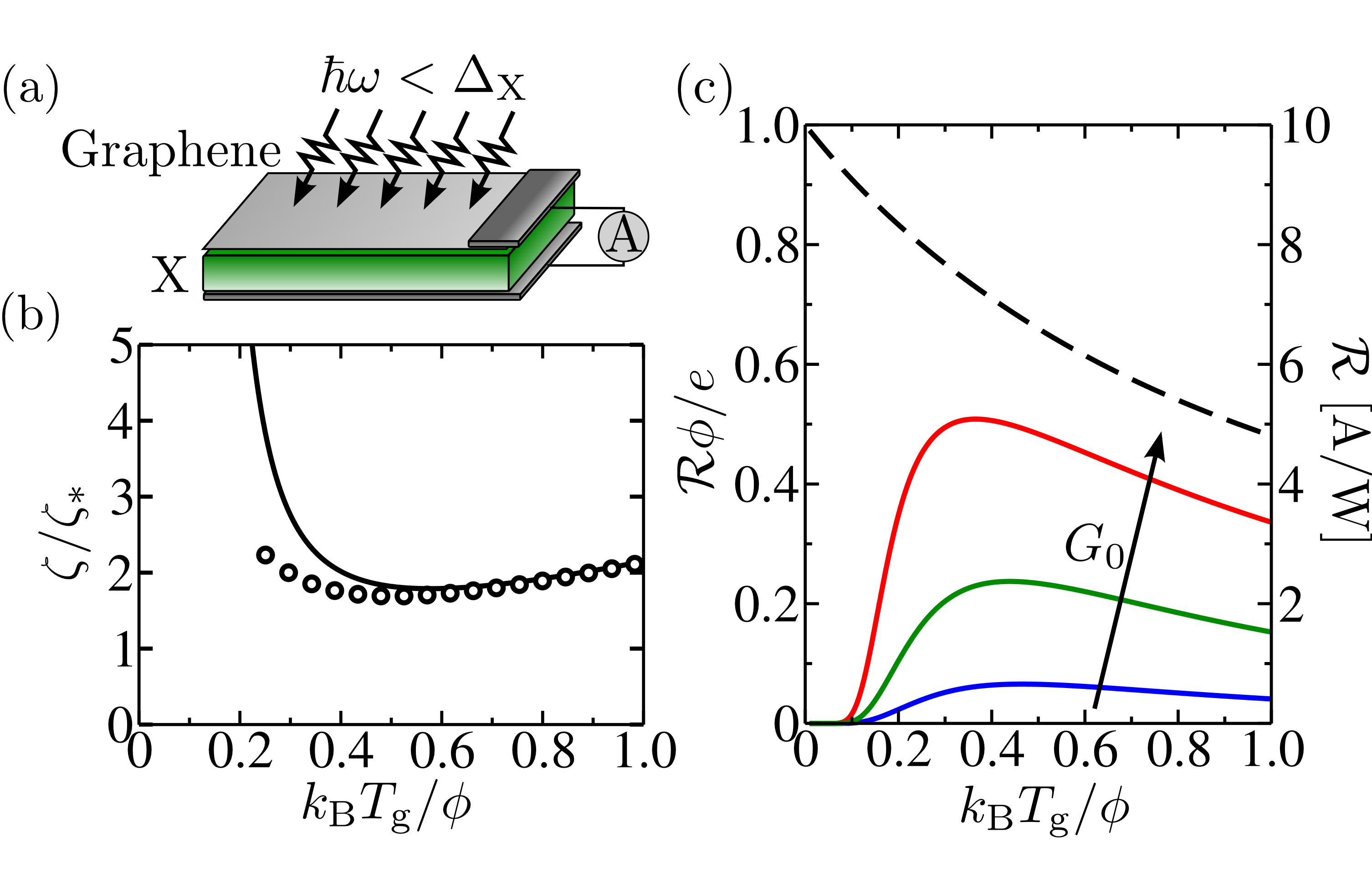
The hot carrier thermionic cooling channel, , and the strong charge-energy current coupling it produces [Eq.(1)], can manifest itself in large and non-monotonic responsivities in g/X photodetectors (Fig. 2a). Accounting for energy balance in Eq.(8) we find a net responsivity given by
| (14) |
where quantifies losses. To estimate for actual devices, we consider the disorder-assisted cooling power in graphene song , as an illustrative example, see Eq.(13). Adopting the same procedure as described above, we find
| (15) |
where the characteristic is set by . As expected, increasing the prefactor , for , increases the losses to phonon scattering embodied in . Alternatively, increasing the conductance across the g/X interface enhances the thermionic channel.
In calculating in Eq.(14), we use the same parameter values as in Fig. 1: and . The value of can be estimated from conductance measured in the dark state, , obtained in actual g/X devices at equilibrium (for example g/Si Schottky junctions in Refs. gschottky1 ; gschottky2 ). Indeed, under an infinitesimally small potential bias , we can approximate in Eq.(11) as due to the small chemical potential difference between G and X. Integrating over in Eq.(11), we obtain . In a typical scenario , the conductance in the dark state is exponentially suppressed with increasing temperature as , in agreement with the qualitative behavior observed in Refs. gschottky1 ; gschottky2 ; gschottky3 ; gsolar ; britnellscience ; ws2heterostructures ; britnellnanolett . To give an estimate of the range of conductances achievable in g/X devices, in these experiments report for with at room temperature. This gives in the ballpark [for in Fig. 2c, we used , which correspond to , see Eq.(15)].
As shown in Fig. 2b, exhibits a clear non-monotonic dependence on characterized by two regimes: (i) small , is exponentially suppressed by the transport barrier , thus dominates, (ii) large , we find that scales as , and rises less steeply than the power law of supercollision cooling. Hence, there is a “sweet spot” for observing a competitive thermionic channel . The optimal value occurs for temperatures (see Fig. 2b), with minimum . This can be estimated from Eq.(15) in the limit and , where the above-mentioned optimal values are obtained from minimization of the equation (Fig. 2b).
The responsivity in Eq.(14) mirrors to display a non-monotonic dependence on , peaking at a temperature , as shown in Fig. 2c. Peak responsivities in the range are obtained within our model. Indeed, for large (corresponding to ), starts to approach the ideal case, (dashed black line). The non-monotonic dependence of as a function of provides a clear fingerprint of the competition between thermionic energy transport and conventional electron-phonon cooling. Since the Schottky barrier heights can be tuned by the applied gate voltage, the peak temperature is gate tunable. Further, the scaling of and the device conductance also provides experimental knobs with which to adjust the responsivity of the device.
The optimal responsivity ocurring at is an important characteristic for the design of graphene photodetectors. Indeed, given that in realistic situations, Schottky barriers in the ballpark allow operation of the g/X photodetector near optimal responsivities (i.e. near minimum ). These values of can be achieved, for instance, in graphene-WS2 devices ws2heterostructures .
Although g/X photodetectors allow in situ control of by electrostatic doping, it is important to note that several parameters of the model vary implicitly with . On the one hand, changes in also induce changes in graphene doping, thus modifying the electronic cooling power. Further, when becomes smaller than the incoming photon energies, photo-emission of primary carriers over the barrier competes with thermalization by electron-electron interactions. In this case, a smaller amount of the incident power is captured in the hot-carrier distribution.
Naturally, there are other mechanisms for losses that affect the responsivity. For instance, lateral (in-plane) heat currents, , can transport heat towards the contacts in small devices. To estimate this effect, we use the Wiedemann-Franz relation, , where is the in-plane electrical conductivity of graphene. For the relevant regime of moderate to high temperatures, , we can approximate [cf. Eq.(7)]. As a result, we find a cooling length coming from the thermionic channel that is independent of . Using a uniform in-plane novoselov , we find , so that vertical energy extraction dominates over in-plane thermal conduction for sufficiently large devices with size .
We note that interactions with the substrate can result in cooling via surface optical phonons. These losses will vary for different substrate (X) choices and are only significant when X is a polar material shytov . Importantly, we do not expect them to be relevant in non-polar materials, e.g. X silicon.
Lastly, it is interesting to note that g/X photodetectors can also operate at low photon energies, . In this regime, conventional Drude absorption from ambient carriers directly captures incident radiation. This contrasts with conventional semiconductor photodetectors, that do not absorb light below the semiconductor bandgap. A tantalizing possibility is to use g/X Schottky junctions within the mid IR - THz bandwidth where presently-available technologies offer lackluster performance chan2007 ; rogalski .
In summary, graphene Schottky junctions host tunable interfaces across which energy transport can be engineered, exemplified by thermionic-dominated transport regime wherein energy and charge currents are strongly coupled. Fingerprints of the thermionic-dominated regime include high responsivities on the order of A/W, and a non-monotonic dependence of on electron temperature (or pump power) in g/X photodetectors. The large degree of in situ tunability allows optimization of the g/X interface for different applications and irradiation conditions; vertical hot carrier convection opens up new vistas to efficiently harvest photon energies over a wide spectral range, utilizing the entire exposed graphene area as a photoactive region.
We are grateful to useful discussions with M. Baldo, M. Kats, L. Levitov. We also thank V. Fatemi, A. Frenzel, and K. Tielrooij for a critical reading. JFRN and MSD acknowledge financial support from the National Science Foundation Grant DMR-1004147. JCWS acknowledges support from a Burke Fellowship at Caltech.
JCWS Current Address: Institute of High Performance Computing Singapore, and Division of Physics and Applied Physics, Nanyang Technological University.
References
- (1) A. K. Geim, I. V. Grigorieva, Nature 499, 7459 (2013).
- (2) X. Miao, S. Tongay, M. K. Petterson, K. Berke, A. G. Rinzler, B. R. Appleton, A. F. Hebard, Nano Letters 12, 2745 (2012).
- (3) X. Wang, Z. Cheng, K. Xu, H. K. Tsang, J.-B. Xu, Nat. Photonics 7, 888 (2013).
- (4) L. Britnell, R. V. Gorbachev, R. Jalil, B. D. Belle, F. Schedin, M. I. Katsnelson, L. Eaves, S. V. Morozov, A. S. Mayorov, N. M. R. Peres, A. H. C. Neto, J. Leist, A. K. Geim, L. A. Ponomarenko, K. S. Novoselov, Nano Letters 12, 1707 (2012).
- (5) W. J. Yu, Z. Li, H. Zhou, Y. Chen, Y. Wang, Y. Huang, Xiangfeng Duan, Nat. Materials 12, 246 (2013).
- (6) X. Li, H. Zhu, K. Wang, A. Cao, J. Wei, C. Li, Y. Jia, Z. Li, D. Wu, Adv. Mater. 22, 2743 (2010).
- (7) C.-C. Chen, M. Aykol, C.-C. Chang, A. F. J. Levi, S. B. Cronin, Nano Letters 11, 1863 (2011).
- (8) H. Yang, J. Heo, S. Park, H. J. Song, D. H. Seo, K.-E. Byun, P. Kim, I. Yoo, H.-J. Chung, K. Kim, Science 336, 1140 (2012).
- (9) L. Britnell, R. V. Gorbachev, R. Jalil, B. D. Belle, F. Schedin, A. Mishchenko, T. Georgiou, M. I. Katsnelson, L. Eaves, S. V. Morozov, N. M. R. Peres, J. Leist, A. K. Geim, K. S. Novoselov, L. A. Ponomarenko, Science 335, 947 (2012).
- (10) T. Georgiou, R. Jalil, B. D. Belle, L. Britnell, R. V. Gorbachev, S. V. Morozov, Y.-J. Kim, A. Gholinia, S. J. Haigh, O. Makarovsky, L. Eaves, L. A. Ponomarenko, A. K. Geim, K. S. Novoselov, A. Mishchenko, Nat Nano 8, 100 (2013).
- (11) A. Di Bartolomeo, Physics Reports 606, 1 (2016).
- (12) R. Bistritzer, A. H. MacDonald, Phys. Rev. Lett. 102 206410 (2009).
- (13) W.-K. Tse, S. Das Sarma, Phys. Rev. B 79, 235406 (2009).
- (14) J. C. W. Song, M. Y. Reizer, L. S. Levitov, Phys. Rev. Lett. 109 106602 (2012).
- (15) M. W. Graham, S.-F. Shi, D. C. Ralph, J. Park, P. L. McEuen, Nature Physics 9, 103 (2013).
- (16) A. C. Betz, S. H. Jhang, E. Pallecchi, R. Ferreira, G. Feve, J.-M. Berroir, B. Placais, Nature Physics 9, 109 (2013).
- (17) N. M. Gabor, J. C. W. Song, Q. Ma, N. L. Nair, T. Taychatanapat, K. Watanabe, T. Taniguchi, L. S. Levitov, P. Jarillo-Herrero, Science 334, 648 (2011).
- (18) Koppens, F. H. L., Mueller, T., Avouris, Ph., Ferrari, A. C., Vitiello, M. S., Polini, M., Nat Nano 9, 780 (2014).
- (19) K. J. Tielrooij, J. C. W. Song, S. A. Jensen, A. Centeno, A. Pesquera, A. Zurutuza Elorza, M. Bonn, L. S. Levitov, F. H. L. Koppens, Nature Physics 9, 248 (2013).
- (20) J. C. W. Song, K. J. Tielrooij, F. H. L. Koppens, L. S. Levitov, Phys. Rev. B 87 155429 (2013).
- (21) S. M. Sze, The physics of semiconductor devices, Wiley, New York (2007).
- (22) R. R. Nair, P. Blake, A. N. Grigorenko, K. S. Novoselov, T. J. Booth, T. Stauber, N. M. R. Peres, and A. K. Geim, Science 320, 1308 (2008).
- (23) K. Rajkanan, R. Singh and J. Shewchun, Solid-State Electronics 22, 793 (1979).
- (24) H. Yan, T. Low, W. Zhu, Y. Wu, M. Freitag, X. Li, F. Guinea, P. Avouris and F. Xia, Nat Photon 7, 394 (2013).
- (25) J. F. Rodriguez-Nieva, M. S. Dresselhaus, and L. S. Levitov, Nano Letters 15, 1451 (2015).
- (26) J. R. Goldman, and J. A. Prybyla, Phys. Rev. Lett. 72 1364 (1994).
- (27) K. S. Novoselov, A. K. Geim, S. V. Morozov, D. Jiang, M. I. Katsnelson, I. V. Grigorieva, S. V. Dubonos and A. A. Firsov, Nature 438, 197 (2005).
- (28) A. S. Price, S. M. Hornett, A. V. Shytov, E. Hendry, D. W. Horsell, Phys. Rev. B 85, 161411 (2012).
- (29) W. L. Chan, J. Deibel, and D. M. Mittleman, Reports on the Progress of Physics 70 1325 (2007).
- (30) A. Rogalski, Infrared Detectors, CRC Press: Boca Raton, Florida (2007).