Photoinduced quantum spin and valley Hall effects and orbital magnetization in monolayer MoS2
Abstract
We theoretically demonstrate that 100% valley-polarized transport in monolayers of MoS2 and other group-VI dichalcogenides can be obtained using off-resonant circularly polarized light. By tuning the intensity of the off-resonant light the intrinsic band gap in one valley is reduced, while it is enhanced in the other valley, enabling single valley quantum transport. As a consequence, we predict (i) enhancement of the longitudinal electrical conductivity, accompanied by an increase in the spin-polarization of the flowing electrons, (ii) enhancement of the intrinsic spin Hall effect, together with a reduction of the intrinsic valley Hall effect, and (iii) enhancement of the orbital magnetic moment and orbital magnetization. These mechanisms provide appealing opportunities to the design of nanoelectronics based on dichalcogenides.
pacs:
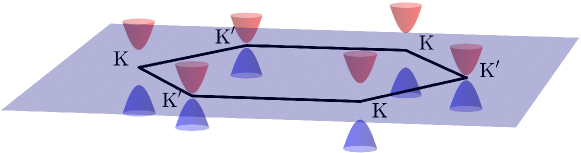
73.63.-b, 72.20.-i, 72.20.Ht, 73.43.-fMonolayers of the transition metal dichalcogenides ( Mo, W; S, Se) are emerging as promising materials for a wide variety of applications in nanoelectronics, due to their exceptional band structures 1 . In particular, the exfoliation of MoS2 monolayers has attracted significant interest since the realization of field-effect-transistors with high on-off ratio 2 . Monolayers of can be regarded as semiconductor analogs of graphene 3 ; 4 , resulting in similar phenomena such Fas spin and valley Hall effects 5 ; 6 . Indeed, MoS2 has a honeycomb lattice with an intrinsic direct band gap of 1 to 2 eV, which is in the visible range. The band-edge is located at the energy degenerate valleys (corners of the hexagonal Brillouin zone) 7 ; 8 .
Thanks to its direct band gap, MoS2 is suitable for optical manipulations and opens access to many optoelectronic applications 7 ; 8 ; 9 . It has been predicted that both valley polarization and valley coherence can be achieved by optical pumping with circularly and linearly polarized light 5 ; 6 ; 10 . First experimental realizations have been reported for MoS2 and WSe2 11 ; 12 ; 13 ; 14 , suggesting that monolayers of could be used for integrated valleytronic devices. Experiments have shown 30% to 50% valley polarization with circularly polarized light in the resonance regime 10 ; 11 ; 12 . Recent works on the optoelectronic properties of MoS2 indicate that the photoresponse of externally biased phototransistors is driven by conductivity alteration upon illumination 15 ; 16 ; 17 . A photovoltaic effect has been reported for MoS2 devices in contact with metallic electrodes that generate large Schottky barriers 18 ; 19 . In addition, ultrasensitive phototransistors with improved mobility have been demonstrated in Ref. 20 . These devices show a photoresponsitivity in the 400 to 680 nm range with a maximum of 880 A/W at a wavelength of 561 nm.
In contrast with the on-resonant optical induction used till now, we propose in this letter a scheme to employ off-resonant light to influence the band structure and corresponding transport properties of monolayers, enabling 100% valley polarization. An important motivation is the development of new experimental probes 21 that make it possible to access non-equilibrium effects, where time-periodic perturbation due to circularly polarized light represents a rich and versatile resource for creating a band gap 22 . An analog has been realized experimentally in a photonic system 23 ; 24 . We show that the band structure of MoS2 is strongly modified by the off-resonant light, resulting in a valley-dependent tuning of the band gap, which is not achievable by on-resonant light. We demonstrate analytically that this valley-dependent band gap results in the emergence of a quantum spin Hall effect, the reduction of the quantum valley Hall effect, and enhancement of the orbital magnetic moment and orbital magnetization.
Off-resonant light cannot generate real photon absorption/emission due to energy conservation, whereas off-resonant light can affect the electron system by second order virtual photon processes (a photon is first absorbed/emitted and then emitted/absorbed). When averaged over time, these processes result in an effective static alteration of the band gap of the system. Therefore, using circularly polarized light, it is possible to distinctively tune the band gap at the and valleys. Off-resonance light-induced gap opening has been predicted for graphene and the surface states of topological insulators 22 as well as for silicene new1 , and has been confirmed experimentally 21 . These studies show that off-resonant light enables quantum phase transitions in two-dimensional systems.
The charge carriers in MoS2 obey a two-dimensional Dirac-like Hamiltonian 5 ; 6 with large intrinsic direct band gap and strong spin-orbit-coupling (SOC). We model MoS2 by an effective Hamiltonian in the -plane in the presence of circularly polarized light,
| (1) |
Here represents the valleys and , respectively, is the mass term that breaks the inversion symmetry, (, , ) is the vector of Pauli matrices (applies to both the valence and conduction bands), is the SOC energy, represents the up and down spins, respectively, and denotes the Fermi velocity of the Dirac fermions. In our notation, the spin-quantization axis is chosen along the -direction. We use the gauge in the two-dimensional canonical momentum , with the vector potential
| (2) |
where is the frequency of the light and with being the amplitude of the electric field . The gauge potential satisfies time periodicity, with . The plus/minus sign refers to right/left circular polarization. As long as the photon energy is much larger than the kinetic energy of the electrons, can be reduced to an effective static (time-independent) Hamiltonian using Floquet theory 22 ; 23 . This method gives results in excellent agreement with experiments 21 ; 23 ; 24 . The effective Hamiltonian is defined through the time evolution operator over one period
| (3) |
where is the time ordering operator. Using perturbation theory and expanding in the limit of large frequencies , we obtain
| (4) |
where is the -th Fourier harmonic of the time-periodic Hamiltonian. Notice that Eq. (4) is only valid under the off-resonance condition ( is the hopping parameter between two nearest neighbors with being the lattice constant) 22 ; new4 . Indeed, when , multiple photon absorption/emission processes must be accounted for, which implies that higher orders in the expansion of should be retained. On the other hand, the condition implies that the frequency must be much larger than the band width of the system, which is difficult to reach in practice. In fact, for such large frequencies, high energy bands might also contribute to the optical processes. In the present work, we focus on the impact of off-resonant light on low energy bands only and assume that any direct optical processes involving high energy bands only weakly affect the low energy band structure. Still, due to the presence of these high energy processes, the effective power of the incident off-resonant light A is reduced.
Applying on Eq. (1), Eq. (4) yields
| (5) |
where is the effective energy term describing the effects of the circularly polarized light, which essentially renormalizes the mass of the Dirac fermions. The plus/minus sign refers to right/left circular polarization. For right circular polarization the gap is increased in the valley and reduced in the valley, whereas for left circular polarization the effect is opposite. After diagonalization we obtain the eigenvalues
| (6) |
and the corresponding eigenfunctions
| (7) |
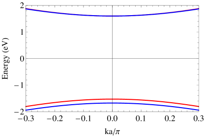
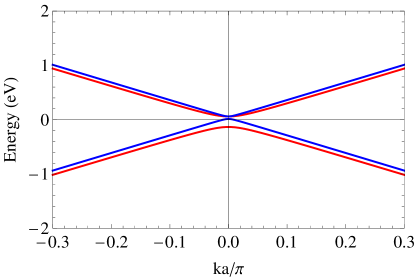
Here represents the conduction and valence bands, respectively, with , and . The impact of off-resonant light on the band structure is illustrated in Figs. 1 and 2 for MoS2 ( eV, eV, m/s, Å, and eV 5 ). We set , which corresponds to a gap variation of eV for eV. Such a large value of ensures that the low energy bands are only affected by virtual emission/absorption processes, while higher energy processes are assumed to only affect the effective power of the incident light (see also Refs. 22 ; new1 ; new4 ). The energy correction can be tuned by varying the amplitude of the electric field or frequency of the light.
Two aspects are worth noticing. First, as mentioned above, the effect of the off-resonant light is to enhance the gap for the valley and reduce it for the valley ( eV and eV in our example). In this case only one valley (here ) becomes relevant for electronics purposes, enabling almost 100% valley polarization of the transport. Second, the SOC-induced splitting is enhanced in the conduction band, while it remains essentially unchanged in the valence band. Indeed, in the absence of off-resonant light the SOC is only active in the valence bands and leaves the conduction bands almost unaffected. The reduction of the band gap in the valley correspondingly empowers SOC-induced splitting in the conduction bands which become spin-polarized. Nevertheless, we stress that due to the fact that the two valence bands () are non-degenerate at it is still possible to obtain fully spin-polarized hole transport by tuning the Fermi level, while the conduction band can be at most partially spin-polarized. Since the system is fully valley-polarized, only the conduction band of the valley () contributes to the transport properties discussed in this work.
We calculate the longitudinal conductivity using the Kubo formula and perform a perturbative expansion in terms of the short-range impurity potential within the first Born approximation. We use the Streda 26 version of the Kubo formula 27
| (8) |
where the velocity components () are given by and . The superscript minus represents the valley, is the Fermi distribution function, and are the advanced and retarded perturbed Green’s functions. The unperturbed retarded Green’s function is given by . Using Eq. (5) with , we obtain
| (9) |
The perturbed Green’s function is given by , where is the retarded self-energy. Considering short range randomly distributed impurities in the first Born approximation, we have
| (10) |
where is the impurity concentration and is the impurity potential. We obtain
| (11) |
where is the energy broadening due to the finite quasi-particle lifetime . Using Eq. (11) in Eq. (8) and addressing the limit of zero temperature with chemical potential , we arrive at
| (12) |
As expected, the conductivity is enhanced under off-resonant light, since the effective band gap is reduced. More interestingly, the gap reduction is accompanied by a spin-polarization of the longitudinal electron flow. Indeed, since the mass of the carriers is reduced, the impact of SOC is stronger, leading to a polarization
| (13) |
The intrinsic Hall conductivity due to anomalous trajectories of free electrons under the action of the electric field is expressed in terms of the Berry curvature in -space as 5 ; 27 ; 28
| (14) |
where denotes the Fermi distributions of the electrons and holes, respectively. From Eqs. (6) and (7), we obtain the Berry curvature as
| (15) |
Using Eq. (15) in Eq. (14) and performing the integral over k, we obtain the intrinsic Hall conductivity when the Fermi level is in the band gap (indicated by a subscript 0)
| (16) |
which yields the quantum spin and valley Hall effects. For we have , which results in a vanishing quantum spin Hall effect and finite quantum valley Hall effect . For we have , which results in a vanishing quantum valley Hall effect and finite quantum spin Hall effect . Using meV we obtain for meV a value of eV for eV, which may be varied by alteration of via the intensity of the off-resonant light and is consistent with Fig. 2. These results can be compared with Ref. 6 where the quantum spin Hall effect is zero in the limit of zero off-resonant light, while the quantum valley Hall effect is similar to what we obtain above in Eq. (16), see Eq. (12d) of Ref. 6 . Note that the SOC is stronger in WS2 (107.5 meV) than in MoS2 (37.5 meV) so that the quantum spin Hall effect is easier to detect 5 .
When the Fermi level is in the conduction band (indicated by a subscript 1), the Hall conductivity is
| (17) |
This anomalous conductivity is similar to that reported in Refs. 5 ; 6 in the limit . However, the valley selectivity introduced by the circularly polarized off-resonant light dramatically changes the situation. Indeed, as mentioned in Refs. 5 ; 6 , for monolayer MoS2 in the absence of off-resonant light both valleys contribute equally to the spin and valley Hall conductivities. However, in the presence of off-resonant light, since the effective band gap becomes valley-dependent, the spin Hall effect is dominated by one valley only ( in the present case) so that it is enhanced, while the valley Hall effect is correspondingly reduced. Since the system is fully valley-polarized, only the conduction band contributes, so that the spin () and valley () Hall conductivities are
| (18) |
When the gap is quenched () the spin Hall effect is simply proportional to the longitudinal polarization, see Eq. (13). The spin and valley Hall conductivies obtained from Eq. (18) can be compared to their counterparts and in the absence of light (see, e.g., Eq. (12e) in Ref. 6 ) and we obtain
| (19) |
which explicitly reveals the role of the light-induced gap. The extrinsic corrections to the anomalous velocity from side jump and skew scattering have been explicitly calculated in the case of a gapped two-dimensional Dirac Hamiltonian in Ref. 27 . Interestingly, they vanish when the chemical potential approaches the gap. By its large gap (1.66 eV), this is the case for MoS2. Additionally, skew scattering contributions are inversely proportional to the impurity concentration and thus vanish in the limit of strong impurity scattering, compare Ref. new3 .
The last aspect to be discussed is the enhancement of the orbital magnetic moment. Indeed, in classical electromagnetism, charges moving with a velocity along a loop of diameter generate an orbital magnetic moment . Recently, values up to have been reported in 5 nm wide carbon nanotubes 29 . In general, while the orbital contribution to the magnetization is vanishingly small in 3 transition metal ferromagnets, it turns out to become significant in systems involving orbital degrees of freedom such as nanotubes and graphene-like structures 28 ; 30 . The orbital magnetic moment can be related to the Berry curvature through the relation 28 ; 30
| (20) |
For finite or the orbital magnetic moment has a peak at . For zero SOC we obtain for meV a single valley orbital magnetic moment of 35 Bohr magnetons. This may be varied by alteration of by modifying the intensity of the off-resonant light. The orbital magnetic moment turns out to be inversely proportional to the band gap.
The corresponding orbital magnetization is 28 ; 30
| (21) |
and we calculate analytically
| (22) |
Interestingly, this expression has a similar structure as the Hall conductivity, Eq. (17), and can be enhanced by reducing the band gap using off-resonant light. As a reference, for a Fermi energy of 100 meV and a layer thickness of typically 0.6 nm, we would have an orbital magnetization of 0.05 Tesla, which is easily detectable and tunable by varying . The orbital magnetization can be probed by various experimental techniques, including susceptibility measurements, electron paramagnetic resonance, x-ray magnetic circular dichroism, and neutron diffraction 31 ; 32 ; 33 . The orbital contribution to the magnetization affects a variety of properties and phenomena such as the nuclear magnetic resonance 34 and electron paramagnetic resonance 35 g-tensors, which both are related to the derivative of the orbital magnetization as well as to the magnetic susceptibility, the orbital magnetoelectric response 36 ; 37 ; 38 , and the quantum spin Hall conductivity 39 .
We propose to use off-resonant circularly polarized light to enable valley-polarized nanoelectronics in group-VI dichalcogenide monolayers such as MoS2. We theoretically demonstrate that under such illumination the band gaps of the and valleys are oppositely tuned, leading to 100% valley polarization. This phenomenon leads to a number of remarkable effects: (i) Enhancement of the longitudinal conductivity, accompanied by an increase in the spin-polarization of the flowing electrons, (ii) enhancement of the intrinsic spin Hall effect, together with a reduction of the intrinsic valley Hall effect, and (iii) enhancement of the orbital magnetic moment and orbital magnetization. Our predictions cna be realized experimentally by the setup used in Ref. new5 for studying WS2. The discussed findings expand the horizon of fundamental investigations of the electronic properties of two-dimensional dichalcogenide systems and presents promising opportunities to the design of tunable phototransistors 15 ; 16 ; 17 ; 18 ; 19 ; 20 , photothermoelectric devices 40 , and related transport devices.
Acknowledgements.
A. M. acknowledges fruitful discussions with Dr. T. Korn.References
- (1) A. K. Geim and I. V. Grigorieva, Nature 499, 419 (2013).
- (2) B. Radisavljevic, A. Radenovic, J. Brivio, V. Giacometti, and A. Kis, Nat. Nanotechnol. 6, 147 (2011).
- (3) K. S. Novoselov, A. K. Geim, S. Morozov, D. Jiang, Y. Zhang, S. Dubonos, I. Grigorieva, and A. A. Firsov, Science 306, 666 (2004).
- (4) A. H. Castro Neto, F. Guinea, N. M. R. Peres, K. S. Novoselov, and A. K. Geim, Rev. Mod. Phys. 81, 109 (2009).
- (5) D. Xiao, G.-B. Liu, W. Feng, X. Xu, and W. Yao, Phys. Rev. Lett. 108, 196802 (2012).
- (6) Z. Li and J. P. Carbotte, Phys. Rev. B 86, 205425 (2012).
- (7) K. F. Mak, C. Lee, J. Hone, J. Shan, and T. F. Heinz, Phys. Rev. Lett. 105, 136805 (2010).
- (8) A. Splendiani, L. Sun, Y. Zhang, T. Li, J. Kim, C. Y. Chim, G. Galli, and F. Wang, Nano Lett. 10, 1271 (2010).
- (9) A. Kuc, N. Zibouche, and T. Heinz, Phys. Rev. B 83, 245213 (2011).
- (10) T. Cao, G. Wang, W. Han, H. Ye, C. Zhu, J. Shi, Q. Niu, P. Tan, E. Wang, B. Liu, and J. Feng, Nat. Commun. 3, 887 (2012).
- (11) K. F. Mak, K. He, J. Shan, and T. F. Heinz, Nat. Nanotechnol. 7, 494 (2012).
- (12) H. Zeng, J. Dai, W. Yao, D. Xiao, and X. Cui, Nat. Nanotechnol. 7, 490 (2012).
- (13) S.Wu, J. S. Ross,G.-B. Liu, G. Aivazian, A. Jones, Z. Fei, W. Zhu, D. Xiao, W. Yao, D. Cobden, and X. Xu, Nat. Phys. 9, 149 (2013).
- (14) A. M. Jones, H. Yu, N. J. Ghimire, S. Wu, G. Aivazian, J. S. Ross, B. Zhao, J. Yan, D. G. Mandrus, D. Xiao, W. Yao, and X. Xu, Nat. Nanotechnol. 8, 634 (2013).
- (15) Z. Yin, H. Li, L. Jiang, Y. Shi, Y. Sun, G. Lu, Q. Zhang, X. Chen, H. Zhang, ACS Nano 6, 74 (2012).
- (16) H. S. Lee, S. W. Min, Y. G. Chang, M. K. Park, T. Nam, H. Kim, J. H. Kim, S. Ryu, and S. Im, Nano Lett. 12, 3695 (2012).
- (17) W. Choi, M. Y. Cho, A. Konar, J. H. Lee, G. -B. Cha, S. C. Hong, S. Kim, J. Kim, D. Jena, J. Joo, S. Kim, Adv. Mater. 24, 5832 (2012).
- (18) M. Fontana, T. Deppe, A. K. Boyd, M. Rinzan, A. Y. Liu, M. Paranjape, and P. Barbara, Sci. Rep. 3, 1634 (2013).
- (19) M. Shanmugam, C. A. Durcan, B. Yu, Nanoscale 4, 7399 (2012).
- (20) O. L. Sanchez, D. Lembke, M. Kayci, A. Radenovic, and A. Kis, Nat. Nanotechnol. 8, 497 (2013).
- (21) Y. H. Wang, H. Steinberg, P. J. Herrero, and N. Gedik, Science 342, 453 (2013).
- (22) T. Kitagawa, T. Oka, A. Brataas, L. Fu, E. Demler, Phys. Rev. B 84, 235108 (2011).
- (23) T. Kitagawa, M. A. Broome, A. Fedrizzi, M. S. Rudner, E. Berg, I. Kassal, A. A. Guzik, E. Demler, and A. G. White, Nat. Commun. 3, 882 (2012).
- (24) M. C. Rechtsman, J. M. Zeuner, Y. Plotnik, Y. Lumer, D. Podolsky, F. Dreisow, S. Nolte, M. Segev, and A. Szameit, Nature 496, 196 (2013).
- (25) K. F. Mak, C. Lee, J. Hone, J. Shan, and T. F. Heinz, Phys. Rev. Lett. 105, 136805 (2010).
- (26) M. Ezawa, Phys. Rev. Lett. 110, 026603 (2013).
- (27) Á. Gómez-León, P. Deplace, and G. Platero, Phys. Rev. B 89, 205408 (2014).
- (28) J. S. Barriga, A. Varykhalov, J. Braun, S.-Y. Xu, N. Alidoust, O. Kornilov, J. Minar, K. Hummer, G. Springholz, G. Bauer, R. Schumann, L. V. Yashina, H. Ebert, M. Z. Hasan, and O. Rader, Phys. Rev. X 4, 011046 (2014).
- (29) P. Streda, J. Phys. C 15, L717 (1982).
- (30) N. A. Sinitsyn, J. E. Hill, H. Min, J. Sinova, and A. H. MacDonald, Phys. Rev. Lett. 97, 106804 (2006).
- (31) D. Xiao, W. Yao, and Q. Niu, Phys. Rev. Lett. 99, 236809 (2007).
- (32) S. Onoda, N. Sugimoto, and N. Nagaosa, Phys. Rev. Lett. 97, 126602 (2006).
- (33) E. D. Minot, Y. Yaish, V. Sazonova, and P. L. McEuen, Nature 428, 536 (2004).
- (34) T. Thonhauser, Int. J. Mod. Phys. B 25, 1429 (2011).
- (35) L. L. Hirsh, Rev. Mod. Phys. 69, 607 (1997).
- (36) R. M. White, Quantum Theory of Magnetism (Springer, Berlin, 2007).
- (37) Magnetism and Synchrotron Radiation, edited by E. Beaurepaire, H. Bulou, F. Scheurer, and J.-P. Kappler, Springer Proceedings in Physics Vol. 133 (Springer, Berlin, 2010). See also the references therein.
- (38) T. Thonhauser, D. Ceresoli, A. A. Mostofi, N. Marzari, R. Resta, and D. Vanderbilt, J. Chem. Phys. 131, 101101 (2009).
- (39) D. Ceresoli, U. Gerstmann, A. P. Seitsonen, and F. Mauri, Phys. Rev. B 81, 060409(R) (2010).
- (40) A. M. Essin, J. E. Moore, and D. Vanderbilt, Phys. Rev. Lett. 102, 146805 (2009).
- (41) A. Malashevich, I. Souza, S. Coh, and D. Vanderbilt, New J. Phys. 12, 053032 (2010).
- (42) A. M. Essin, A. M. Turner, J. E. Moore, and D. Vanderbilt, Phys. Rev. B 81, 205104 (2010).
- (43) S. Murakami, Phys. Rev. Lett. 97, 236805 (2006).
- (44) E. J. Sie, J. W. McIver, Y.-H. Lee, L. Fu, J. Kong, and N. Gedik, ArXiv:1407.1825 (2014).
- (45) M. Buscema, M. Barkelid, V. Zwiller, H. S. J. van der Zant, G. A. Steele, and A. C. Gomez, Nano Lett. 13, 358 (2013).