Size dependent line broadening in the emission spectra of single GaAs
quantum dots:
Impact of surface charges on spectral diffusion
Abstract
Making use of droplet epitaxy, we systematically controlled the height of self-assembled GaAs quantum dots by more than one order of magnitude. The photoluminescence spectra of single quantum dots revealed the strong dependence of the spectral linewidth on the dot height. Tall dots with a height of 30 nm showed broad spectral peaks with an average width as large as meV, but shallow dots with a height of 2 nm showed resolution-limited spectral lines ( eV). The measured height dependence of the linewidths is in good agreement with Stark coefficients calculated for the experimental shape variation. We attribute the microscopic source of fluctuating electric fields to the random motion of surface charges at the vacuum-semiconductor interface. Our results offer guidelines for creating frequency-locked photon sources, which will serve as key devices for long-distance quantum key distribution.
pacs:
78.67.Hc, 78.55.Cr, 73.21.LaIntroduction. Numerous photonic applications using semiconductor quantum dots rely on the discrete and delta-function-like density of states Michler (2003); *michler_book09. However, various single dot spectroscopy studies have confirmed significant line broadening in the photoluminescence spectra that is normally much broader than the transform limited width determined by the spontaneous emission rate. The line broadening mechanism is commonly attributed to spectral diffusion, where the transition frequency randomly changes through the fluctuation of a local electric field in the vicinity of dots Empedocles, Norris, and Bawendi (1996); *Empedocles_JPC99; Blanton, Hines, and Guyot-Sionnest (1996); Seufert et al. (2000); Türck et al. (2000). The fluctuating spectral line becomes integrated into a relatively broad peak thanks to the long time scales of signal integration compared with those of environmental motion.
Some progress has been made in studying the short time scale dynamics of the spectral fluctuation. Photon correlation measurement can elucidate spectrally diffusive photoluminescence with subnanosecond characteristic times Sallen et al. (2010); *Sallen_PRB11; Abbarchi et al. (2012). The correlation functions routinely show monoexponent decays, which implies efficient coupling between a single dot and a small number of environment configurations. In contrast, resonant fluorescence measurements reveal broad-band noise spectra in the Hz to 100 kHz range, where contributions can be expected from a large number of environment configurations Kuhlmann et al. (2013). Photon counting statistics of resonant fluorescence further reveal the Gaussian distribution of the random environmental shifts, which might be a consequence of the central limit theorem adopted for a large ensemble Matthiesen et al. (2014). By contrast, high-resolution Fourier transform measurement confirms a motionally narrowed Lorentzian lineshape associated with rapid environmental fluctuation Berthelot et al. (2006). More recent work on field-effect devices identifies charge traps at the barrier/well interface Houel et al. (2012) or impurity centers Hauck et al. (2014) as a dominant field source. Thus, the timescales and magnitudes of spectral diffusion vary greatly depending on the sample and the measurement conditions. We still lack a global understanding of the microscopic mechanism of spectral diffusion, however it is needed for developing frequency-locked photon sources as basic elements in long-distance quantum key distribution, e.g., quantum repeaters for extending the key transmission distance.
In this work we experimentally analyze the dependence of quantum dot morphology on environment-mediated spectral broadening. For this purpose we focus on GaAs quantum dots grown by droplet epitaxy, which enables us to continuously control the quantum dot height by more than one order of magnitude. The morphology tunability contrasts with that of traditional quantum dot growth using the Stranski-Krastanow mode, where the dot profile is essentially fixed by strain relaxation and surface energies. The spectral linewidth of a single dot emission depends strongly on the dot height. The measured height dependence agrees with that of Stark coefficients along the growth direction (normal to the sample surface). We attribute the source of the electric field fluctuation to the change in the microscopic configuration of surface charges at the vacuum-semiconductor interface Wang et al. (2004); Majumdar, Kim, and Vučković (2011). Thus, morphology engineering is an alternative route to achieving narrower emitter linewidths without the need for feedback techniques to suppress spectral fluctuation Prechtel et al. (2013); Hansom et al. (2014).
Experimental procedure. GaAs quantum dots were self-assembly grown in Al0.3Ga0.7As by droplet epitaxy on semi-insulating GaAs(100) substrates Watanabe, Koguchi, and Gotoh (2000); Mano et al. (2009). These dots are free from strain thanks to the negligible lattice mismatch between GaAs and Al0.3Ga0.7As. After the growth of a 100 nm Al0.3Ga0.7As layer, different amounts of gallium () with 1.5, 2, 3, 5, 7.5, or 10 monolayers (ML) were deposited at 0.5 ML/s and 200 ∘C. This step enabled the formation of gallium droplets. Then, an As4 flux was supplied at Torr and 200 ∘C, and the gallium droplets were fully crystalized to GaAs dots. Note that the As4 flux was roughly two orders of magnitude higher than that used for the self-assembly of quantum ring structures Mano et al. (2005); *Kuroda_PRB05.
After the dots were grown, the sample was annealed at 400 ∘C in situ (under a weak As4 supply) for 10 min, and partially capped with a 20 nm Al0.3Ga0.7As layer. The temperature was then increased to 580 ∘C, while the capping continued with a 30 nm Al0.3Ga0.7As layer followed by a 10 nm GaAs layer. GaAs dots on a 2 ML Al0.3Ga0.7As layer were additionally grown on the top of samples for atomic force microscopy (AFM) analysis. Finally, rapid thermal annealing was carried out at 800 ∘C for 4 min in a N2 atmosphere. All the samples with different amounts of exhibited well-defined dots; see AFM top views in Supplementary Fig. 1. The dot density depended only slightly on from cm-2 (1.5 ML) to cm-2 (10 ML). Thus, we assume that the volumes per dot are nearly proportional to .
We used a continuous-wave laser that emitted at a wavelength of 532 nm as an excitation source. The laser illumination generated photocarriers in the Al0.3Ga0.7As barrier. The excitation polarization was set to be linear in order to avoid a spectral shift of nuclear origin Belhadj et al. (2008); Sallen et al. (2014). Our confocal setup combined an objective lens with a numerical aperture of and a hemispherical solid immersion lens (SIL) with a refractive index of two. The use of the high-index SIL enabled us to reduce the focusing diameter to m Yoshita et al. (1998), where approximately 25 dots were inside the spot. The excitation density was kept sufficiently low so that the carrier population was less than , and the influence of strong optical injection on line broadening was fairly removed. Photoluminescence signals were fed into a spectrometer of a 50 cm focusing length, and analyzed with a full width at half maximum (FWHM) resolution of 120 eV. All the experiments were carried out at 10 K.
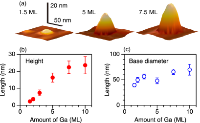
Morphology analysis. Figure 1(a) shows AFM three-dimensional views whose height increases significantly with the amount of . Figures 1(b) and 1(c) show the average dot height and the base diameter, respectively, which were determined by statistical analysis. When the amount of was increased from 1.5 to 10 ML, the dot height increased from to nm, i.e., by a factor of ten. In contrast, the base size increased only by a factor of less than two. Thus, the dot height increased considerably as the dot volume increased, while the base size remained almost unchanged. The mechanism responsible for the volume-dependent aspect ratio is explained in terms of the two-step crystallization process involved in droplet epitaxy, see Supplementary Discussion.
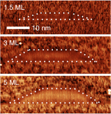
Figure 2 shows the morphology of GaAs quantum dots capped with an Al0.3Ga0.7As matrix that was measured using cross-sectional scanning tunneling microscopy (X-STM) Bocquel et al. (2014). They have a truncated pyramidal shape, which agrees with the AFM cross-sections of uncapped dots. Thus, GaAs dots are embedded in Al0.3Ga0.7As while maintaining their original shape. This is due to the small diffusion length of aluminum atoms, which further gives rise to the formation of a distinct dot-barrier interface. This observation is in stark contrast to commonly studied InAs/GaAs dot systems, where indium atoms diffuse efficiently, and composition mixing leads to the deformation of dots with capping. This shape conservation allows the determination of the shape of embedded dots from AFM measurements of free-standing references
Photoluminescence spectra. Figure 3(a) shows the spectra of a large ensemble of quantum dots. They were measured using long-focus optics. The spectral peaks at eV originate from impurity-bound excitons in the GaAs substrate. Signals associated with quantum dots are observed at 1.85, 1.8, and 1.67 eV in the 1.5, 2, and 5 ML samples, respectively. The emission peak, therefore, shifts to a lower energy side with increasing droplet volume. The 7.5 ML sample shows a relatively narrow peak at 1.55 eV, which is close to the bulk band gap of GaAs.
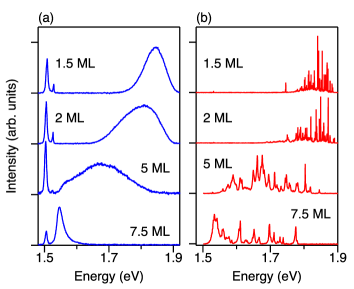
Figure 3(b) shows the emission spectra of a small ensemble of quantum dots that were spatially selected using a micro objective setup. The spectra of both the 1.5 and 2 ML samples consist of sharp lines, whose linewidths are close to, or less than, the instrumental response of our spectrometer. There are around 70 spectral lines, which is approximately three times the expected number of dots inside a focusing spot. The discrepancy is reasonable because each dot is able to generate three to four emission lines through the formation of different types of charged/neutral exciton complexes Abbarchi et al. (2010).
In contrast, the 5 and 7.5 ML samples exhibit relatively broad peaks that dominate the emission signals at energies below 1.75 eV. Note that a few sharp lines are also observed at energies higher than 1.8 eV, as found with the spectral lines of the 1.5 and 2 ML samples. Thus, the broad peaks for low-energy dots and narrow peaks for high-energy dots are not sample-specific signatures, but universal size-dependent behaviors.
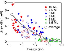
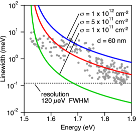
Figure 4 shows linewidth statistics as a function of emission energy. Here we evaluate the FWHM of all the spectral lines by fitting without distinguishing between the neutral and charged transitions. Such treatment is sufficient to clarify the general trend of size-dependent broadening, since the difference between the neutral and charged exciton linewidths is much smaller than the observed dot-to-dot variation, as confirmed previously Abbarchi et al. (2008). The compiled statistics demonstrate a clear correlation between line broadening and emission energy. The smooth transition over the data points of different samples confirms that the linewidth reaches several meV for tall dots, and decreases monotonically to the resolution limit with decreasing dot height. The similar linewidth dependence on emission energies has recently been reported for polar nitride quantum dots Kindel et al. (2014).
Environment-induced line broadening. The effect of the environment on spectral shifts is twofold. First, hyperfine coupling between an electron and nuclei induces the Overhauser field, which acts as an effective magnetic field in the tens of mT range Urbaszek et al. (2013). Second, a charge distribution in the vicinity of dots induces a local electric field. However, the effect of nuclear fluctuation on line broadening is considered to be negligible at least in the present samples, because a typical value for a nuclear field is 10 mT, which corresponds to a spectral shift of 0.25 eV for GaAs Sallen et al. (2014). This is much smaller than the observed linewidth, which reaches several meV. Thus, the following discussion deals only with the effect of electric field fluctuation on line broadening.
A local electric field has various microscopic origins. A common example of a field source is charge particles trapped in impurities or defects. However, their densities are normally very low in samples grown with molecular beam epitaxy (MBE, cm-3). Hence, it is difficult for the bulk impurities or defects to realize line broadening that are comparable to the measured spectra, as also discussed later. Despite the charging and discharging of trapping centers close to dots, here we propose the fluctuation of charge carriers trapped by the vacuum-semiconductor interface as a field source.
The formation of surface states, which trap charge carriers, is linked to the presence of electronically active defects at the vacuum-semiconductor interface Bardeen (1947). It is known that the surface state density depends on orientations and chemical treatments, and reaches cm-2 for a naturally oxidized GaAs(100) surface Nannichi et al. (1988). Charge carriers are efficiently trapped by the surface states, and induce a local electric field normal to the surface on average. The phenomenon also serves as the origin of band bending and Fermi-level pinning Yu and Cardona (2010). When the sample is optically excited, some of the photoinjected carriers recombine with surface charges, and others occupy different surface states. Consequently, the microscopic charge arrangement changes randomly, which gives rise to field fluctuation and spectral broadening through time integration. The effect is orientation dependent, and taller dots become more sensitive to the induced field.
Size-dependent Stark coefficients. Qualitative explanation of the measured line broadening is based on the derivation of Stark coefficients and the simulation of field fluctuation. The Stark shift of a single-particle level is described by the second-order perturbation of the interaction Hamiltonian, i.e.,
| (1) |
where is an electric field, and are the single particle eigen energies of the ground state and the th excited state, respectively, and is a dipole moment along a direction parallel to the field. The above equation demonstrates the size dependence of Stark shifts, where the dipole moment is proportional to the confinement length , the energy denominator is scaled by , hence the Stark coefficient is enhanced as the fourth power of the effective dot size along a built-in field.
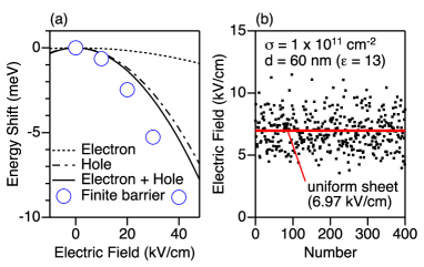
Figure 5(a) shows the field dependence of spectral shifts calculated for a 12-nm-high GaAs dots. The lines show the analytic dependence for a model based on infinite-potential quantum boxes with , and the circles are the results obtained with a more precise model, which takes account of the finite GaAs/Al0.3Ga0.7As potential and the effect of valence-band mixing in terms of four-band perturbation. Both models exhibit parabolic dependence, as expected. Enhanced shifts in the finite-potential dot with respect to the infinite-potential dot arise due to the extended wave function. These results imply that an energy shift as large as 1 meV, which is a typical linewidth in the measured spectra, requires a field strength of the order of 10 kV/cm, which is expected at a position only nm from a point charge. Accompanying impurities or defects in such close proximity to dots is fairly uncommon for MBE grown samples. This is why we have excluded bulk trapping centers and proposed surface charges as a field source.
Simulation of field fluctuation. We evaluate the field fluctuation using a Monte Carlo simulation, where an electric field is induced by randomly positioned charge particles in a flat layer. Figure 5(b) shows the field strength distribution at a point 60 nm from the surface (dielectric constant ). This condition reproduces the geometry of our structure. We found that the field changes randomly with different charge arrangements. The statistics yields a mean field strength of 7 kV/cm and a standard deviation of 1.4 kV/cm for a charge density of cm-2. The validity of this simulation is confirmed by the agreement between the observed mean strength and the value predicted for a uniform charge sheet, , where denotes a charge density. We performed the simulation for different values of , and found that the magnitude of field fluctuation is nearly proportional to .
We assume that transfers proportionally to line broadening , i.e.,
| (2) |
The substitution of Eq. 1 into Eq. 2 yields the line broadening dependence on the transition energy of dots, see Supplementary Discussion for calculation details. Figure 6 compares the experimental linewidths and the calculated spectral fluctuation for different charge densities. There is fairly good agreement between the experimental widths and calculated broadening when the charge density is of the order of cm-2, which is a reasonable value Yablonovitch et al. (1987).
Note that the lower bound of the measured linewidths is limited by our spectrometer resolution, though a previous investigation on similar dot systems using a higher-resolution spectrometer revealed the linewidths as large as a few tens of eV at wavelengths around 1.8 eV Mano et al. (2009). Note also that the model curves exceed the measured linewidths at low energies. These inconsistent asymptotes are attributed to the fact that the present model ignored the effect of Coulomb binding. The quantum confined Stark shifts are associated with the wavefunction separation between electrons and holes. Coulomb attraction would inhibit such separation, and suppress energy shifts. The upper bound of line broadening is therefore roughly limited by the exciton binding energies, which were predicted to be a few tens of meV for GaAs/AlGaAs dots Abbarchi et al. (2010).
Conclusions. Spectral diffusion in the photoluminescence of single quantum dots is an interesting phenomenon that bridges microscopic random dynamics and macroscopic optical response. Here we studied morphologically controlled GaAs quantum dots grown by droplet epitaxy to understand the source of environmental fluctuation, and demonstrated the impact of fluctuating surface charges on dot line broadening.
From a technological point of view, however, the line broadening phenomenon is unfavorable for practical applications of quantum dots to photon emitting devices. The present results suggest several ways to engineer spectral broadening. First, we expect to suppress line broadening by creating dots with a sufficiently low aspect ratio that are robust as regards a random electric field normal to surface. Second, we expect to achieve narrower spectra by embedding dots more deeply in the barrier matrix, where the effect of random charges at the surface would be effectively smoothed out. Line broadening is expected to decrease with the inverse of the dot-surface distance, see Supplementary Figure 3 for the simulation result. Finally, the use of a substrate with a chemically stable surface, such as a gallium terminated (111)A surface Xu et al. (2009); Mano et al. (2010); *Kuroda_PRB13; Ha et al. (2014); *Liu_PRB14, and/or defect passivation technologies Nannichi et al. (1988); Yablonovitch et al. (1987); Robertson, Guo, and Lin (2015) are another potential route by which to reduce surface charge fluctuation.
This work was partially supported by Grant-in-Aid from Japan Society for the Promotion of Science.
References
- Michler (2003) P. Michler, ed., Single Quantum Dots: Fundamentals, Applications and New Concepts, Topics in Applied Physics (Springer, 2003).
- Michler (2009) P. Michler, ed., Single Semiconductor Quantum Dots, NanoScience and Technology (Springer, 2009).
- Empedocles, Norris, and Bawendi (1996) S. A. Empedocles, D. J. Norris, and M. G. Bawendi, “Photoluminescence spectroscopy of single CdSe nanocrystallite quantum dots,” Phys. Rev. Lett. 77, 3873 (1996).
- Empedocles and Bawendi (1999) S. A. Empedocles and M. G. Bawendi, “Influence of spectral diffusion on the line shapes of single CdSe nanocrystallite quantum dots,” J. Chem. Phys. B 103, 1826–1830 (1999).
- Blanton, Hines, and Guyot-Sionnest (1996) S. A. Blanton, M. A. Hines, and P. Guyot-Sionnest, “Photoluminescence wandering in single CdSe nanocrystals,” Appl. Phys. Lett. 69, 3905 (1996).
- Seufert et al. (2000) J. Seufert, R. Weigand, G. Bacher, T. Kümmell, A. Forchel, K. Leonardi, and D. Hommel, “Spectral diffusion of the exciton transition in a single self-organized quantum dot,” Appl. Phys. Lett. 76, 1872 (2000).
- Türck et al. (2000) V. Türck, S. Rodt, O. Stier, R. Heitz, R. Engelhardt, U. W. Pohl, D. Bimberg, and R. Steingrüber, “Effect of random field fluctuations on excitonic transitions of individual CdSe quantum dots,” Phys. Rev. B 61, 9944–9947 (2000).
- Sallen et al. (2010) G. Sallen, A. Tribu, T. Aichele, R. André, L. Besombes, C. Bougerol, M. Richard, S. Tatarenko, K. Kheng, and J.-P. Poizat, “Subnanosecond spectral diffusion measurement using photon correlation,” Nat. Photon. 4, 696–699 (2010).
- Sallen et al. (2011) G. Sallen, A. Tribu, T. Aichele, R. André, L. Besombes, C. Bougerol, M. Richard, S. Tatarenko, K. Kheng, and J.-P. Poizat, “Subnanosecond spectral diffusion of a single quantum dot in a nanowire,” Phys. Rev. B 84, 041405 (2011).
- Abbarchi et al. (2012) M. Abbarchi, T. Kuroda, T. Mano, M. Gurioli, and K. Sakoda, “Bunched photon statistics of the spectrally diffusive photoluminescence of single self-assembled GaAs quantum dots,” Phys. Rev. B 86, 115330 (2012).
- Kuhlmann et al. (2013) A. V. Kuhlmann, J. Houel, A. Ludwig, L. Greuter, D. Reuter, A. D. Wieck, M. Poggio, and R. J. Warburton, “Charge noise and spin noise in a semiconductor quantum device,” Nat. Phys. 9, 570–575 (2013).
- Matthiesen et al. (2014) C. Matthiesen, M. J. Stanley, M. Hugues, E. Clarke, and M. Atatüre, “Full counting statistics of quantum dot resonance fluorescence,” Sci. Rep. 4, 4911 (2014).
- Berthelot et al. (2006) A. Berthelot, I. Favero, G. Cassabois, C. Voisin, C. Delalande, P. Roussignol, R. Ferreira, and J. M. Gérard, “Unconventional motional narrowing in the optical spectrum of a semiconductor quantum dot,” Nat. Phys. 2, 759–764 (2006).
- Houel et al. (2012) J. Houel, A. V. Kuhlmann, L. Greuter, F. Xue, M. Poggio, B. D. Gerardot, P. A. Dalgarno, A. Badolato, P. M. Petroff, A. Ludwig, D. Reuter, A. D. Wieck, and R. J. Warburton, “Probing single-charge fluctuations at a interface using laser spectroscopy on a nearby ingaas quantum dot,” Phys. Rev. Lett. 108, 107401 (2012).
- Hauck et al. (2014) M. Hauck, F. Seilmeier, S. E. Beavan, A. Badolato, P. M. Petroff, and A. Högele, “Locating environmental charge impurities with confluent laser spectroscopy of multiple quantum dots,” Phys. Rev. B 90, 235306 (2014).
- Wang et al. (2004) C. F. Wang, A. Badolato, I. Wilson-Rae, P. M. Petroff, E. Hu, J. Urayama, and A. Imamoğlu, “Optical properties of single InAs quantum dots in close proximity to surfaces,” Appl. Phys. Lett. 85, 3423–3425 (2004).
- Majumdar, Kim, and Vučković (2011) A. Majumdar, E. D. Kim, and J. Vučković, “Effect of photogenerated carriers on the spectral diffusion of a quantum dot coupled to a photonic crystal cavity,” Phys. Rev. B 84, 195304 (2011).
- Prechtel et al. (2013) J. H. Prechtel, A. V. Kuhlmann, J. Houel, L. Greuter, A. Ludwig, D. Reuter, A. D. Wieck, and R. J. Warburton, “Frequency-stabilized source of single photons from a solid-state qubit,” Phys. Rev. X 3, 041006 (2013).
- Hansom et al. (2014) J. Hansom, C. H. H. Schulte, C. Matthiesen, M. J. Stanley, and M. Atatüre, “Frequency stabilization of the zero-phonon line of a quantum dot via phonon-assisted active feedback,” Appl. Phys. Lett. 105, 172107 (2014).
- Watanabe, Koguchi, and Gotoh (2000) K. Watanabe, N. Koguchi, and Y. Gotoh, “Fabrication of GaAs quantum dots by modified droplet epitaxy,” Jpn. J. Appl. Phys. 39, L79 (2000).
- Mano et al. (2009) T. Mano, M. Abbarchi, T. Kuroda, C. A. Mastrandrea, A. Vinattieri, S. Sanguinetti, K. Sakoda, and M. Gurioli, “Ultra-narrow emission from single GaAs self-assembled quantum dots grown by droplet epitaxy,” Nanotechnology 20, 395601 (2009).
- Mano et al. (2005) T. Mano, T. Kuroda, S. Sanguinetti, T. Ochiai, T. Tateno, J. Kim, T. Noda, M. Kawabe, K. Sakoda, G. Kido, and N. Koguchi, “Self-assembly of concentric quantum double rings,” Nano Lett. 5, 425–428 (2005).
- Kuroda et al. (2005) T. Kuroda, T. Mano, T. Ochiai, S. Sanguinetti, K. Sakoda, G. Kido, and N. Koguchi, “Optical transitions in quantum ring complexes,” Phys. Rev. B 72, 205301 (2005).
- Belhadj et al. (2008) T. Belhadj, T. Kuroda, C.-M. Simon, T. Amand, T. Mano, K. Sakoda, N. Koguchi, X. Marie, and B. Urbaszek, “Optically monitored nuclear spin dynamics in individual GaAs quantum dots grown by droplet epitaxy,” Phys. Rev. B 78, 205325 (2008).
- Sallen et al. (2014) G. Sallen, S. Kunz, T. Amand, L. Bouet, T. Kuroda, T. Mano, D. Paget, O. Krebs, X. Marie, K. Sakoda, and B. Urbaszek, “Nuclear magnetization in gallium arsenide quantum dots at zero magnetic field,” Nat Commun 5, 3268 (2014).
- Yoshita et al. (1998) M. Yoshita, T. Sasaki, M. Baba, and H. Akiyama, “Application of solid immersion lens to high-spatial resolution photoluminescence imaging of GaAs quantum wells at low temperatures,” Appl. Phys. Lett. 73, 635–637 (1998).
- Bocquel et al. (2014) J. Bocquel, A. D. Giddings, T. Mano, T. J. Prosa, D. J. Larson, and P. M. Koenraad, “Composition profiling of GaAs/AlGaAs quantum dots grown by droplet epitaxy,” Appl. Phys. Lett. 105, 153102 (2014).
- Abbarchi et al. (2010) M. Abbarchi, T. Kuroda, T. Mano, K. Sakoda, C. A. Mastrandrea, A. Vinattieri, M. Gurioli, and T. Tsuchiya, “Energy renormalization of exciton complexes in GaAs quantum dots,” Phys. Rev. B 82, 201301(R) (2010).
- Abbarchi et al. (2008) M. Abbarchi, F. Troiani, C. Mastrandrea, G. Goldoni, T. Kuroda, T. Mano, K. Sakoda, N. Koguchi, S. Sanguinetti, A. Vinattieri, and M. Gurioli, “Spectral diffusion and line broadening in single self-assembled GaAs/AlGaAs quantum dot photoluminescence,” Appl. Phys. Lett. 93, 162101 (2008).
- Kindel et al. (2014) C. Kindel, G. Callsen, S. Kako, T. Kawano, H. Oishi, G. Hönig, A. Schliwa, A. Hoffmann, and Y. Arakawa, “Spectral diffusion in nitride quantum dots: Emission energy dependent linewidths broadening via giant built-in dipole moments,” Phys. Status Solidi Rapid Res. Lett. 8, 408–413 (2014).
- Urbaszek et al. (2013) B. Urbaszek, X. Marie, T. Amand, O. Krebs, P. Voisin, P. Maletinsky, A. Högele, and A. Imamoglu, “Nuclear spin physics in quantum dots: An optical investigation,” Rev. Mod. Phys. 85, 79–133 (2013).
- Bardeen (1947) J. Bardeen, “Surface states and rectification at a metal semi-conductor contact,” Phys. Rev. 71, 717–727 (1947).
- Nannichi et al. (1988) Y. Nannichi, J.-F. Fan, H. Oigawa, and A. Koma, “A model to explain the effective passivation of the GaAs surface by (NH4)2Sx treatment,” Jpn. J. Appl. Phys. 27, L2367 (1988).
- Yu and Cardona (2010) P. Y. Yu and M. Cardona, “Fundamentals of semiconductors,” (Springer, 2010) Chap. 8.3.
- Yablonovitch et al. (1987) E. Yablonovitch, C. J. Sandroff, R. Bhat, and T. Gmitter, “Nearly ideal electronic properties of sulfide coated GaAs surfaces,” Appl. Phys. Lett. 51, 439–441 (1987).
- Xu et al. (2009) M. Xu, Y. Q. Wu, O. Koybasi, T. Shen, and P. D. Ye, “Metal-oxide-semiconductor field-effect transistors on GaAs (111)A surface with atomic-layer-deposited Al2O3 as gate dielectrics,” Appl. Phys. Lett. 94, 212104 (2009).
- Mano et al. (2010) T. Mano, M. Abbarchi, T. Kuroda, B. McSkimming, A. Ohtake, K. Mitsuishi, and K. Sakoda, “Self-assembly of symmetric GaAs quantum dots on (111)A substrates: Suppression of fine-structure splitting,” Appl. Phys. Express 3, 065203 (2010).
- Kuroda et al. (2013) T. Kuroda, T. Mano, N. Ha, H. Nakajima, H. Kumano, B. Urbaszek, M. Jo, M. Abbarchi, Y. Sakuma, K. Sakoda, I. Suemune, X. Marie, and T. Amand, “Symmetric quantum dots as efficient sources of highly entangled photons: Violation of Bell’s inequality without spectral and temporal filtering,” Phys. Rev. B 88, 041306 (2013).
- Ha et al. (2014) N. Ha, X. Liu, T. Mano, T. Kuroda, K. Mitsuishi, A. Castellano, S. Sanguinetti, T. Noda, Y. Sakuma, and K. Sakoda, “Droplet epitaxial growth of highly symmetric quantum dots emitting at telecommunication wavelengths on InP(111)A,” Appl. Phys. Lett. 104, 143106 (2014).
- Liu et al. (2014) X. Liu, N. Ha, H. Nakajima, T. Mano, T. Kuroda, B. Urbaszek, H. Kumano, I. Suemune, Y. Sakuma, and K. Sakoda, “Vanishing fine-structure splittings in telecommunication-wavelength quantum dots grown on (111)A surfaces by droplet epitaxy,” Phys. Rev. B 90, 081301 (2014).
- Robertson, Guo, and Lin (2015) J. Robertson, Y. Guo, and L. Lin, “Defect state passivation at III-V oxide interfaces for complementary metal-oxide-semiconductor devices,” J. Appl. Phys. 117, 112806 (2015).