Present Address:]Kavli Institute of Nanoscience, Delft University of Technology, 2600 GA Delft, The Netherlands.
Impact of Heterostructure Design on Transport Properties in the Second Landau Level of in-situ Back-Gated Two-Dimensional Electron Gases
Abstract
We report on transport in the second Landau level in in-situ back-gated two-dimensional electron gases in GaAs/AlxGa1-xAs quantum wells. Minimization of gate leakage is the primary heterostructure design consideration. Leakage currents resulting in dissipation as small as 10 pW can cause noticeable heating of the electrons at 10 mK, limiting the formation of novel correlated states. We show that when the heterostructure design is properly optimized, gate voltages as large as 4V can be applied with negligible gate leakage, allowing the density to be tuned over a large range from depletion to over 4 1011 cm-2. As a result, the strength of the state can be continuously tuned from onset at n cm-2 to a maximum mK at n = cm-2. An unusual evolution of the reentrant integer quantum Hall states as a function of density is also reported. These devices can be expected to be useful in experiments aimed at proving the existence of non-Abelian phases useful for topological quantum computation.
I Introduction
Since the discovery of the fractional quantum Hall effect (FQHE) at Willett et al. (1987), this state has drawn intense scrutiny. Much of the motivation for the study of the state comes from the fact that numerical work Morf (1998); Rezayi and Haldane (2000); Peterson et al. (2008); Storni et al. (2010) has shown strong overlaps with the Pfaffian wavefunction Moore and Read (1991) and its particle-hole conjugate state, the so-called anti-Pfaffian Lee et al. (2007); Levin et al. (2007), both of which are non-Abelian and could find uses in topologically protected quantum computation Kitaev (2003); Das Sarma et al. (2005); Nayak et al. (2008). There have also, however, been theoretically proposed wavefunctions for the state that exhibit Abelian statistics (see Bishara et al. (2009); Yang and Feldman (2013) for a summary of candidate states). To date, the experimental tests to determine the nature of the ground state at have failed to agree on the identity of the wavefunction. Experiments probing the temperature dependence of tunneling between the edge states at have been proposed Fendley et al. (1995) and conducted Radu et al. (2008); Lin et al. (2012) as a way to measure the quasiparticle effective charge and Luttinger liquid interaction parameter in order to discriminate between proposed wavefunctions. These experiments, however, were inconclusive as tunneling experiments performed on the same Hall bar mesa but with different electrostatic confinement potentials gave results consistent with the non-Abelian anti-Pfaffian and states Radu et al. (2008) and the Abelian 331 state Lin et al. (2012). Later experients by a different group Baer et al. (2014) were most consistent with the 331 state, but recent measurements of the spin polarization at using NMR techniques Tiemann et al. (2012); Stern et al. (2012) indicate a fully spin-polarized electron gas which is inconsistent with the unpolarized 331 state Halperin (1983). Interferometry experiments showing an alternating Aharanov-Bohm period Willett et al. (2009, 2010) are also consistent with a non-Abelian state at and thus appear to rule out the 331 state. As it is unclear how possible edge reconstruction Chamon and Wen (1994) due to shallow confining potentials might influence the interpretation of the tunneling experiments, it is possible that the different confinement parameters in the previously studied devices could be responsible for this apparent discrepancy.
Given the complications associated with these experiments, it would therefore be desirable to examine transport in nanostructures in the quantum Hall regime in samples in which the electron density and confining potential could be tuned simultaneously in a single structure. A variable density would also allow for direct comparisons between experimental results in the 2 Landau level (LL) and the more well-understood lowest LL in a single device without the need for extremely large magnetic fields. In addition, the original proposal de C. Chamon et al. (1997) for an edge-state interferometer designed to directly measure the quantum statistics of the quasiparticles at called for a device with a global back-gate to allow magnetic field sweeps at a constant filling fraction. As such, there is strong motivation for back-gated devices exhibiting strong FQHE in the 2 LL concomitant with a large range of density tuneability.
II Device Growth and Fabrication
In order to undertake such experiments, however, it is necessary to have a thorough understanding of how heterostructure design and device fabrication parameters affect device yields and the quality of transport in the 2 LL. Towards this aim, we have grown and processed a series of high quality, in-situ backgated two-dimensional electron gases (2DEGs). The processing of similar devices of lower mobility has been reported Meirav et al. (1988); Ritchie et al. (1991); Hamilton et al. (1992); Hirayama et al. (1998); Kawaharazuka et al. (2000); Muraki et al. (2000); Kawaharazuka et al. (2001); Valeille et al. (2008) and a similar high mobility device has been used to examine the energy gaps of FQHE states in the 2 LL Nuebler et al. (2010). However, to our knowledge there has not been a published systematic study of heterostructure design and processing conditions and their impact on the visibility of states in the 2 LL.
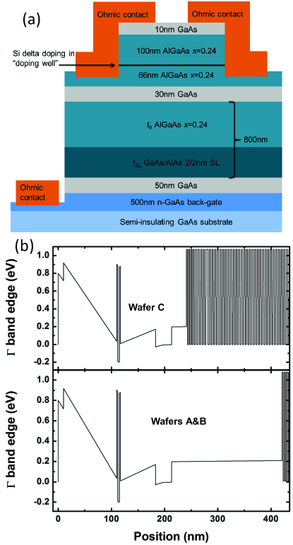
We studied three wafers utilizing two heterostructure designs summarized in Fig. 1 to study the impact of the heterostructure on the gate leakage and the low temperature transport. Both designs feature a 2DEG located approximately 200 nm from the surface in a 30 nm GaAs quantum well flanked by Al0.24Ga0.76As barriers modulation doped from the top side only at a setback of 70 nm. The dopants were incorporated in a so-called doping well scheme (also known as a short-period superlattice) Eisenstein et al. (2002); Pfeiffer and West (2003); Umansky et al. (2009); Manfra (2014) which has been found empirically to maximize the FQHE energy gaps in the 2 LL. The in-situ gate consisted of an n+ GaAs layer situated 850 nm below the bottom interface of the quantum well. The key difference between the two designs was that in design #1 an Al0.24Ga0.76As barrier of thickness nm separated the quantum well from a GaAs/AlAs (2/2 nm) superlattice while in design #2 was decreased to 20 nm while keeping the overall gate setback fixed at 850 nm. Wafers A and B utilized design #1 while wafer C utilized design #2.
Device fabrication began by etching via holes to the gate layer using an etchant consisting of 50:5:1 water:phosphoric:peroxide followed by a second, 160 nm deep etch to define 1 mm Van der Pauw square mesas. Ohmic contacts consisted of a 8/80/160/36 nm stack of Ni/Ge/Au/Ni and were annealed for 1 min in forming gas at a variety of temperatures. Following the annealing, large TiAu pads off of the mesa were deposited in order to facilitate wirebonding.
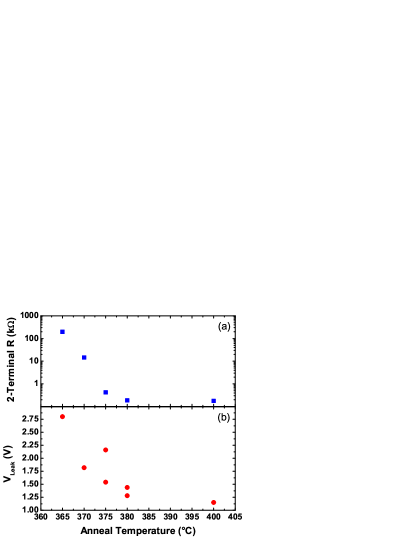
Figure 2 shows the effect of annealing temperature on the quality of the contacts and the gate leakage measured in the dark at T = 4 K on devices fabricated from wafer B. The lead resistance of the measurement setup was 1 , so the 2-terminal resistance values quoted here are reasonable proxies for the true contact resistance. At an annealing temperature of 360 ∘C, the contacts were electrically open at low temperature, and the contact morphology was extremely smooth, indicating that the metal did not melt or diffuse significantly during the anneal. Figure 2b displays the effect of the annealing on the gate leakage. To quantify the leakage from our devices, we defined V as the gate voltage V at which the gate leakage current reached 1 nA; thus high values of V are expected for a high quality gate insulating layer. Both the 2-terminal resistance and V decrease monotonically as the annealing temperature is increased and the NiAuGe diffuses further into the semiconductor.
To further study the impact of mask design and processing parameters on the gate leakage and contact resistance, we fabricated a set of test structures (not shown) which gave evidence that the gate leakage was primarily through the annealed contacts and not through the bulk of the mesa. In addition, the test structures gave evidence that the leakage current density through annealed metal in etched regions was larger than that through annealed metal in un-etched regions. The increased electric field due to the decreased gate-contact separation in the etched regions was insufficient to account for this increase in leakage density. This observation appears to imply that the etching procedure enhances the subsequent diffusion of the contacts. With this in mind, we designed our lithographic mask sets to minimize the total Ohmic area, particularly in the region off of the etched mesa. In our final design the total Ohmic area was 1.5 104 m2 per device, and the total Ohmic overhang off each mesa was 6000 m2. By minimizing the total time the etched sidewall of the mesa was exposed to air between the etch step and the metallization (typically 3-4 hours) and optimizing the geometry of the Ohmic contacts to include 45∘ scallops, we were able to produce devices with acceptably low contact resistances in the range of a few hundred Ohms while minimizing the gate leakage.

Next, we examined the impact of heterostructure design on device performance. Using our optimized fabrication recipe and mask set, we fabricated devices on both wafers B and C, using an annealing temperature of 375 ∘C. Figure 3 is a histogram of the leakage turn-on V for devices from each wafer. The leakage in the majority of devices from wafer B (black bars) turned on around 2.2 V while the leakage in devices from wafer C (red bars) typically turned on around 3.8 V. Evidently, the proximity of the superlattice to the quantum well has a pronounced effect on the gate leakage.
The dashed line in Fig. 3 represents the gate voltage required in our geometry to reach a 2DEG density of 3.2 1011 cm-2, roughly twice the zero-bias density and the approximate electron density of 2DEGs exhibiting state-of-the-art energy gaps in the 2 LL (see for instance references Deng et al. (2014); Samani et al. (2014); Manfra (2014)). As the devices from wafer C clearly could be biased well beyond the point necessary to study the FQHE of the 2 LL, we fabricated Hall bar devices with larger contacts on wafer C to check how much less stringent the device design and fabrication requirements were for this wafer to exhibit acceptable gate leakage. These devices were based on a design Miller et al. (2007) known to both exhibit high quality transport in the 2 LL and allow the incorporation of nanostructures. The total Ohmic area per device was 3.0 105 m2 with 4.6 104 m2 overhanging the edge of the mesa. Even though the Ohmic area in the etch field increased by a factor of 8 and the total Ohmic area increased by a factor of 20 from our optimized mask design, the leakage turn-on in most devices was still beyond 2.5 V, further highlighting the importance of proper heterostructure design.
We speculate that the large reduction in gate leakage in wafer C is due to two effects. First, the alternating layers of the superlattice act as a diffusion barrier Petroff et al. (1984); Schaff et al. (1984) to the metal from the Ohmic contacts; thus, by moving the superlattice closer to the quantum well, less metal is able to diffuse towards the gate, thereby reducing the shorting of the Ohmics to the gate. In addition, Fowler-Nordheim tunneling Lenzlinger and Snow (1969); Weinberg (1982); Smoliner et al. (1987); Hickmott et al. (1984); Jensen (2003) from the bulk of the 2DEG to the gate can be expected to be reduced by moving the tall AlAs barriers of the superlattice closer to the 2DEG.
While moving the superlattice closer to the quantum well has the benefit of dramatically increasing the maximum achievable density, it also has the undesirable consequence of placing a significant amount of AlAs close to the quantum well. It is known that Al is an effective getter of vacuum impurities during MBE growth Pfeiffer and West (2003), and thus moving the superlattice closer to the 2DEG may degrade the quality of the FQHE states. Indeed, the average maximum electron mobility in devices from wafer B was cm2/Vs while that from wafer C was cm2/Vs. Wafers B and C were grown on the same day, so it appears likely that the decrease in mobility can be attributed to the change in heterostructure design. That being said, it has become clear in recent years that the zero field mobility is not a good predictor of energy gaps in the 2 LL Nuebler et al. (2010); Deng et al. (2014); Das Sarma and Hwang (2014); Manfra (2014). Consequently, it was necessary to examine the magnetotransport at low temperature to make any definitive statement on the potential negative impact of moving the superlattice closer to the 2DEG.
III Impact of Heat Sinking and Heterostructure Design on RIQHE States

Figure 4 illustrates the importance of minimizing the gate leakage and properly heat sinking the sample in order to study the 2 LL at low temperatures (T mK). The data shown were taken from an early device from wafer A which was fabricated prior to the final optimization of our processing recipe. During the first cool down of the device, the Joule heating of the electrons due to the gate leakage current evidently caused the electron temperature to depart from the mixing chamber temperature T for a gate leakage current (power) 4 pA ( 3.5 pW) as evinced by weakening of the reentrant integer quantum Hall effect (RIQHE) features (data not shown). By contrast, the excitation current of 2.1 nA contributed a neglible power dissipation of 45 fW at . In order to facilitate wire bonding, we mounted the device on a commercial bondable ceramic chip carrier during the first cool-down. This meant, however, that the sample was only cooled through the 18 m thick Au bond wires. To improve the heat sinking, we re-wired the same device on a homemade header. In this design the sample was mounted to a strip of Cu with Ag paint, and the Cu strip was screwed directly onto the Cu cold finger of the mixing chamber resulting in a continuous metal connection between the mixing chamber and sample. With this improved heat sinking, heating of the electrons was not evident until a gate leakage current (power) 56 pA (67pW). Figure 4 illustrates the vast improvement in electron temperature achieved by improving the heat sinking of the sample. For a fixed density and approximately constant gate leakage current, the data taken with the Cu strip header show strong RIQHE features while the data taken with the ceramic chip carrier shows no RIQHE features. To quantify T during the first cool-down, we show data (green curve in Fig. 4) taken at T = 51 mK during the second cooldown. The insulating peaks in R in the vicinity of at T = 51 mK during the second cool-down are comparable to those seen at T = 11 mK during the first cool-down. This allows us to estimate T 50 mK for the black curves in Fig. 4.
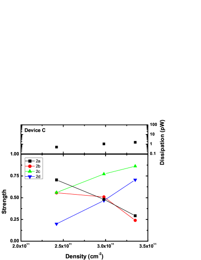
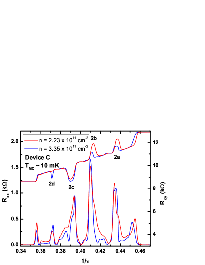
After optimizing our fabrication recipe, we cooled one exemplary device each from wafers B (device B) and C (device C) to low temperature ( mK) to examine the transport as a function of density at low temperature. The RIQHE states in device C (from wafer C) showed an interesting evolution with density as shown in Fig. 5. In order to quantitatively compare the states, we defined the strength of the RIQHE states as
| (1) |
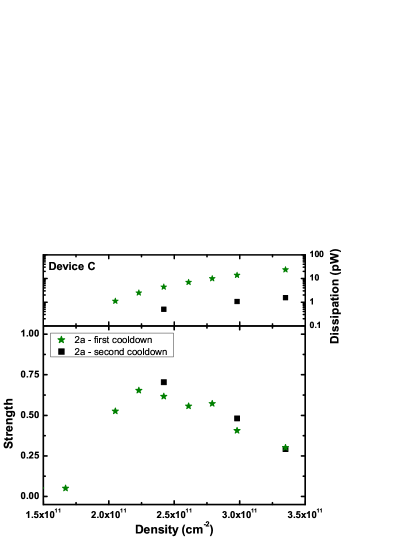
where is the the classical Hall resistance at the filling fraction of interest, is the actual Hall resistance at the peak position, and is the resistance of the nearest integer Hall plateau. Using this definition, a fully quantized RIQHE state has a strength of 1 while a completely absent state has a strength of 0. Figure 5 shows the evolution of the RIQHE states in device C during its second cool-down. The states on the high field side of , 2a and 2b ( 2.29 and 2.42, respectively), are seen to weaken over the measured density range while states 2c and 2d ( 2.56 and 2.70, respectively) continue to strengthen. Figure 6 shows a comparison of the evolution of state 2a in device C as a function of density for two different cooldowns. Even though the power dissipation from the gate leakage varied by 1 order of magnitude between the two cool-downs (possibly due to slightly different illumination conditions), the data show the same trend. Comparisons between the other three states for the two cool-downs show similar agreement. This appears to indicate that the observed evolution in strength is driven primarily by the 2DEG density and not by heating from the gate leakage. At present, the origin of this behavior is not understood. Regardless of the mechanism that causes states 2a and 2b to weaken with increasing density, this behavior is qualitatively different than that seen in states 2c and 2d and may point to a difference in the underlying localization mechanisms. In contrast, the strength of all the RIQHE states in device B (from wafer B) with the larger superlattice setback (data not shown) were seen to increase with density up to a density (power dissipation) of cm-2 (6.4 pW) after which all the RIQHE states weakened. While we cannot identify the mechanisms that alter localization, it appears that the different proximity of the superlattice to the 2DEG in wafers B and C has a significant impact.
| Device | P1 (pW) | P2 (pW) |
|---|---|---|
| A - Copper Header | 1.5 | 67 |
| B - Copper Header | 6.4 | 114 |
| C - Copper Header | 1.6 | 38 |
Finally, to estimate the maximum acceptable power dissipation, we summarize the measured data points on either side of the heating threshold at which all the RIQHE states started to weaken with increasing density in Table 1. Given that the maximum strength in device B was observed for a power dissipation of 6.4 pW and the RIQHE states in device C had begun to weaken by 38 pW, we set 10 pW as the upper bound on acceptable power dissipation from the gate in our devices given the setup of our cryostat. This extremely low power level serves to highlight the necessity of minimizing the gate leakage in order to study the 2 LL.
IV Impact of Heterostructure Design on the FQHE states
We now turn to the central result of our work. Figure 7 shows low temperature transport (T 10 mK) at two different densities for device C after illumination with a red LED. The device shows excellent transport with all four RIQHE states present and well developed FQHE states at = 14/5, 8/3, 5/2, and 7/3. In addition, nascent states at and begin to develop at high density. This is, to our knowledge, the first time these states have been observed in a back-gated device, and their presence in spite of their extreme fragility Xia et al. (2004); Kumar et al. (2010); Zhang et al. (2012) further points to the high quality of the 2DEG. The presence of the state at is particularly interesting as this state has been proposed as a host of Fibonacci anyons which could be used for universal topological quantum computation Nayak et al. (2008).
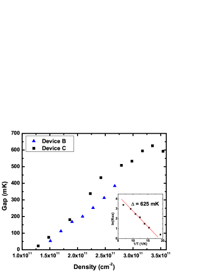
We examined the strength of the FQHE in each device quantitatively by measuring the gap at (). Figure 8 displays the gap at as a function of density for devices B and C. It is clear that, within the experimental resolution, the gaps are nearly identical for both devices at low density (n cm-2). Evidently, neither the day-to-day variation in the MBE growth conditions nor the uncontrolled sample degradation from device fabrication nor the proximity of the superlattice to the 2DEG significantly affect the gap at . Device C, however, allows investigation of much higher 2DEG densities. Moreover, the magnitude of the gaps are very large with the gap in device C reaching a maximum value of 625 mK, the highest reported to date, at a density of cm-2.
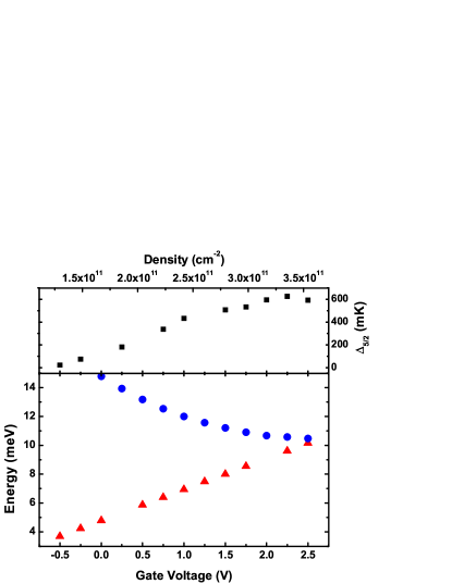
One noticeable feature of the data from device C in Fig. 8 is that at the highest density measured the gap shows a pronounced drop. It has been previously reported Liu et al. (2011) that the gap at drops suddenly when the energy difference between the Fermi energy E and the first excited electric sub-band in the quantum well equals the cyclotron energy. In this case, there is a level crossing and the ground state is pushed into the lowest LL of the anti-symmetric sub-band. Figure 9 shows the calculated nex energy spacing along with the cyclotron energy as a function of density. As expected, the experimentally measured gap at is seen to drop suddenly when the cyclotron energy becomes approximately equal to the gap between E and the second sub-band. Taken together, our calculations and experimental data indicate that larger gaps at even higher densities could potentially be achieved if the quantum well were made more narrow to further separate the ground and excited sub-bands.
V Conclusion
To summarize, we have examined the effect of heterostructure design and device processing on the performance of in-situ back-gated 2DEGs in the 2 LL. We found that the position of the GaAs/AlAs superlattice barrier relative to quantum well has a large impact on the leakage characteristics of the device due to its effectiveness in blocking the diffusion of the Ohmic contacts towards the gate and minimizing Fowler-Nordheim tunneling. Moving the superlattice closer to the 2DEG greatly increases the range of low-leakage gating without significantly degrading the strength of the gap at or other correlated states in the 2 LL. In addition, we found that gate leakage dissipation powers as small as a few pW are sufficient to cause electronic heating that impacts transport in the 2 LL. By improving the heat sinking of the lattice, the acceptable power dissipation is increased to 10 pW. Moreover, it is likely that the FQHE gaps would continue to rise at higher density beyond what we report here if the electric sub-bands were spaced sufficiently far apart. Thus, examining gaps as a function of density in narrower quantum wells could potentially yield important results on the density dependence of the gap at other states potentially useful for topological quantum computation such as . As we have demonstrated a robust recipe for these structures and as the FQHE states in the 2 LL are very strong over a wide range of density, these devices should prove useful in experiments intended to test for the presence of non-Abelian statistics in quantum Hall systems.
ACKNOWLEDGEMENTS
This work was supported by the US DOE Office of Basic Energy Sciences, Division of Materials Sciences and Engineering Award DE-SC0006671. J.D.W. thanks L.A. Tracy and R.L. Willett for helpful discussions regarding device processing.
References
- Willett et al. (1987) R. Willett, J. P. Eisenstein, H. L. Störmer, D. C. Tsui, A. C. Gossard, and J. H. English, “Observation of an Even-Denominator Quantum Number in the Fractional Quantum Hall Effect,” Phys. Rev. Lett. 59, 1776 (1987).
- Morf (1998) R. H. Morf, “Transition from Quantum Hall to Compressible States in the Second Landau Level: New Light on the Enigma,” Phys. Rev. Lett. 80, 1505 (1998).
- Rezayi and Haldane (2000) E. H. Rezayi and F. D. M. Haldane, “Incompressible Paired Hall State, Stripe Order, and the Composite Fermion Liquid Phase in Half-Filled Landau Levels,” Phys. Rev. Lett. 84, 4685 (2000).
- Peterson et al. (2008) M. R. Peterson, T. Jolicoeur, and S. Das Sarma, “Finite-Layer Thickness Stabilizes the Pfaffian State for the 5/2 Fractional Quantum Hall Effect: Wave Function Overlap and Topological Degeneracy,” Phys. Rev. Lett. 101, 016807 (2008).
- Storni et al. (2010) M. Storni, R. H. Morf, and S. Das Sarma, “Fractional Quantum Hall State at and the Moore-Read Pfaffian,” Phys. Rev. Lett. 104, 076803 (2010).
- Moore and Read (1991) G. Moore and N. Read, “Nonabelions in the Fractional Quantum Hall Effect,” Nucl. Phys. B 360, 362 (1991).
- Lee et al. (2007) S. -S. Lee, S. Ryu, C. Nayak, and M. P. A. Fisher, “Particle-Hole Symmetry and the Quantum Hall State,” Phys. Rev. Lett. 99, 236807 (2007).
- Levin et al. (2007) M. Levin, B. I. Halperin, and B. Rosenow, “Particle-Hole Symmetry and the Pfaffian State,” Phys. Rev. Lett. 99, 236806 (2007).
- Kitaev (2003) A. Y. Kitaev, “Fault-Tolerant Quantum Computation by Anyons,” Ann. Phys. 303, 2 (2003).
- Das Sarma et al. (2005) S. Das Sarma, M. Freedman, and C. Nayak, “Topologically Protected Qubits from a Possible Non-Abelian Fractional Quantum Hall State,” Phys. Rev. Lett. 94, 166802 (2005).
- Nayak et al. (2008) C. Nayak, S. H. Simon, A. Stern, M. Freedman, and S. Das Sarma, “Non-Abelian Anyons and Topological Quantum Computation,” Rev. Mod. Phys. 80, 1083 (2008).
- Bishara et al. (2009) W. Bishara, P. Bonderson, C. Nayak, K. Shtengel, and J. K. Slingerland, “Interferometric Signature of Non-Abelian Anyons,” Phys. Rev. B 80, 155303 (2009).
- Yang and Feldman (2013) Guang Yang and D. E. Feldman, “Influence of Device Geometry on Tunneling in the Quantum Hall Liquid,” Phys. Rev. B 88, 085317 (2013).
- Fendley et al. (1995) P. Fendley, A. W. W. Ludwig, and H. Saleur, “Exact Nonequilibrium Transport Through Point Contacts in Quantum Wires and Fractional Quantum Hall Devices,” Phys. Rev. B 52, 8934 (1995).
- Radu et al. (2008) I. P. Radu, J. B. Miller, C. M. Marcus, M. A. Kastner, L. N. Pfeiffer, and K. W. West, “Quasi-Particle Properties from Tunneling in the = 5/2 Fractional Quantum Hall State,” Science 320, 899 (2008).
- Lin et al. (2012) X. Lin, C. Dillard, M. A. Kastner, L. N. Pfeiffer, and K. W. West, “Measurements of Quasiparticle Tunneling in the Fractional Quantum Hall State,” Phys. Rev. B 85, 165321 (2012).
- Baer et al. (2014) S. Baer, C. Rössler, T. Ihn, K. Ensslin, C. Reichl, and W. Wegscheider, “Experimental Probe of Topological Orders and Edge Excitations in the Second Landau Level,” Phys. Rev. B 90, 075403 (2014).
- Tiemann et al. (2012) L. Tiemann, G. Gamez, N. Kumada, and K. Muraki, “Unraveling the Spin Polarization of the = 5/2 Fractional Quantum Hall State,” Science 335, 828 (2012) .
- Stern et al. (2012) M. Stern, B. A. Piot, Y. Vardi, V. Umansky, P. Plochocka, D. K. Maude, and I. Bar-Joseph, “NMR Probing of the Spin Polarization of the Quantum Hall State,” Phys. Rev. Lett. 108, 066810 (2012).
- Halperin (1983) B. I. Halperin, “Theory of the Quantized Hall Conductance,” Helv. Phys. Acta 56, 75 (1983).
- Willett et al. (2009) R. L. Willett, L.N. Pfeiffer, and K. W. West, “Measurement Of Filling Factor 5/2 Quasiparticle Interference with Observation of Charge e/4 and e/2 Period Oscillations,” Proc. Natl. Acad. Sci. U.S.A. 106, 8853 (2009).
- Willett et al. (2010) R. L. Willett, L. N. Pfeiffer, and K. W. West, “Alternation and Interchange of e/4 and e/2 Period Interference Oscillations Consistent with Filling Factor 5/2 Non-Abelian Quasiparticles,” Phys. Rev. B 82, 205301 (2010).
- Chamon and Wen (1994) C. de C. Chamon and X. G. Wen, “Sharp and Smooth Boundaries of Quantum Hall Liquids,” Phys. Rev. B 49, 8227 (1994).
- de C. Chamon et al. (1997) C. de C. Chamon, D. E. Freed, S. A. Kivelson, S. L. Sondhi, and X. G. Wen, “Two Point-Contact Interferometer for Quantum Hall Systems,” Phys. Rev. B 55, 2331 (1997).
- Meirav et al. (1988) U. Meirav, M. Heiblum, and F. Stern, Appl. Phys. Lett. 52, 1268 (1988).
- Ritchie et al. (1991) D.A. Ritchie, J.E.F. Frost, D.C. Peacock, E.H. Linfield, A. Hamilton, and G.A.C. Jones, “The Growth and Characterisation of Back-Gated High Mobility Two-Dimensional Electron Gas Structures,” J. Cryst. Growth 111, 300 (1991).
- Hamilton et al. (1992) A. R. Hamilton, J. E. F. Frost, C. G. Smith, M. J. Kelly, E. H. Linfield, C. J. B. Ford, D. A. Ritchie, G. A. C. Jones, M. Pepper, D. G. Hasko, and H. Ahmed, “Back-Gated Split-Gate Transistor: A One-Dimensional Ballistic Channel with Variable Fermi Energy,” Appl. Phys. Lett. 60, 2782 (1992).
- Hirayama et al. (1998) Y. Hirayama, K. Muraki, and T. Saku, “Two-Dimensional Electron Gas Formed in a Back-Gated Undoped Heterostructure,” Appl. Phys. Lett. 72, 1745 (1998).
- Kawaharazuka et al. (2000) A. Kawaharazuka, T. Saku, Y. Hirayama, and Y. Horikoshi, “Formation of a Two-Dimensional Electron Gas in an Inverted Undoped Heterostructure with a Shallow Channel Depth,” J. Appl. Phys. 87, 952 (2000).
- Muraki et al. (2000) K. Muraki, N. Kumada, T. Saku, and Y. Hirayama, “n-GaAs Back-Gated Double-Quantum-Well Structures with Full Density Control,” Jpn. J. Appl. Phys. 39, 2444 (2000).
- Kawaharazuka et al. (2001) A. Kawaharazuka, T. Saku, C. A. Kikuchi, Y. Horikoshi, and Y. Hirayama, “Free GaAs Surfaces Studied Using a Back-Gated Undoped Heterostructure,” Phys. Rev. B 63, 245309 (2001).
- Valeille et al. (2008) A. Valeille, K. Muraki, and Y. Hirayama, “Highly Reproducible Fabrication of Back-Gated GaAs/AlGaAs Heterostructures Using AuGeNi Ohmic Contacts With Initial Ni Layer,” Appl. Phys. Lett. 92, 152106 (2008).
- Nuebler et al. (2010) J. Nuebler, V. Umansky, R. Morf, M. Heiblum, K. von Klitzing, and J. Smet, “Density Dependence of the Energy Gap: Experiment and Theory,” Phys. Rev. B 81, 035316 (2010).
- Eisenstein et al. (2002) J. P. Eisenstein, K. B. Cooper, L. N. Pfeiffer, and K. W. West, “Insulating and Fractional Quantum Hall States in the First Excited Landau Level,” Phys. Rev. Lett. 88, 076801 (2002).
- Pfeiffer and West (2003) L. Pfeiffer and K. W. West, “The Role of MBE in Recent Quantum Hall Effect Physics Discoveries,” Physica E 20, 57 (2003).
- Umansky et al. (2009) V. Umansky, M. Heiblum, Y. Levinson, J. Smet, J. Nuebler, and M. Dolev, “MBE Growth of Ultra-Low Disorder 2DEG with Mobility Exceeding 35 x 106 cm2/vs,” J. Cryst. Growth 311, 1658 (2009).
- Manfra (2014) M. J. Manfra, “Molecular Beam Epitaxy of Ultra-High-Quality AlGaAs/GaAs Heterostructures: Enabling Physics in Low-Dimensional Electronic Systems,” Annu. Rev. Condens. Matter Phys. 5, 347 (2014).
- Deng et al. (2014) N. Deng, G. C. Gardner, S. Mondal, E. Kleinbaum, M. J. Manfra, and G. A. Csáthy, “ Fractional Quantum Hall State in the Presence of Alloy Disorder,” Phys. Rev. Lett. 112, 116804 (2014).
- Samani et al. (2014) M. Samani, A. V. Rossokhaty, E. Sajadi, S. Lüscher, J. A. Folk, J. D. Watson, G. C. Gardner, and M. J. Manfra, “Low-Temperature Illumination and Annealing of Ultrahigh Quality Quantum Wells,” Phys. Rev. B 90, 121405 (2014).
- Miller et al. (2007) J. B. Miller, I. P. Radu, D. M. Zumbuehl, E. M. Levenson-Falk, M. A. Kastner, C. M. Marcus, L. N. Pfeiffer, and K. W. West, “Fractional Quantum Hall Effect in a Quantum Point Contact at Filling Fraction 5/2,” Nat. Phys. 3, 561 (2007).
- Petroff et al. (1984) P. M. Petroff, R. C. Miller, A. C. Gossard, and W. Wiegmann, “Impurity Trapping, Interface Structure, and Luminescence of GaAs Quantum Wells Grown by Molecular Beam Epitaxy,” Appl. Phys. Lett. 44, 217 (1984).
- Schaff et al. (1984) W. J. Schaff, L. F. Eastman, B. Van Rees, and B. Liles, “Superlattice Buffers for GaAs Power MESFET’s Grown by MBE,” J. Vac. Sci. Technol. B 2, 265 (1984).
- Lenzlinger and Snow (1969) M. Lenzlinger and E. H. Snow, “Fowler-Nordheim Tunneling into Thermally Grown SiO2,” J. Appl. Phys. 40, 278 (1969).
- Weinberg (1982) Z. A. Weinberg, “On Tunneling in Metal-Oxide-Silicon Structures,” J. Appl. Phys. 53, 5052 (1982).
- Smoliner et al. (1987) J. Smoliner, R. Christanell, M. Hauser, E. Gornik, G. Weimann, and K. Ploog, “Fowler–Nordheim Tunneling and Conduction-Band Discontinuity in GaAs/GaAlAs High Electron Mobility Transistor Structures,” Appl. Phys. Lett. 50, 1727 (1987).
- Hickmott et al. (1984) T. W. Hickmott, P. M. Solomon, R. Fischer, and H. Morkoç, “Resonant Fowler–Nordheim Tunneling in n-GaAs-Undoped AlxGa1-xAs-n+GaAs Capacitors,” Appl. Phys. Lett. 44, 90 (1984).
- Jensen (2003) K. L. Jensen, “Electron Emission Theory and Its Application: Fowler-Nordheim Equation and Beyond,” J. Vac. Sci. Technol., B 21, 1528 (2003).
- Das Sarma and Hwang (2014) S. Das Sarma and E. H. Hwang, “Mobility Versus Quality in Two-Dimensional Semiconductor Structures,” Phys. Rev. B 90, 035425 (2014).
- Xia et al. (2004) J. S. Xia, W. Pan, C. L. Vicente, E. D. Adams, N. S. Sullivan, H. L. Stormer, D. C. Tsui, L. N. Pfeiffer, K. W. Baldwin, and K. W. West, “Electron Correlation in the Second Landau Level: A Competition Between Many Nearly Degenerate Quantum Phases,” Phys. Rev. Lett. 93, 176809 (2004).
- Kumar et al. (2010) A. Kumar, G. A. Csáthy, M. J. Manfra, L. N. Pfeiffer, and K. W. West, “Nonconventional Odd-Denominator Fractional Quantum Hall States in the Second Landau Level,” Phys. Rev. Lett. 105, 246808 (2010).
- Zhang et al. (2012) C. Zhang, C. Huan, J. S. Xia, N. S. Sullivan, W. Pan, K. W. Baldwin, K. W. West, L. N. Pfeiffer, and D. C. Tsui, “Spin Polarization of the Fractional Quantum Hall State,” Phys. Rev. B 85, 241302 (2012).
- Deng et al. (2012) N. Deng, A. Kumar, M. J. Manfra, L. N. Pfeiffer, K. W. West, and G. A. Csáthy, “Collective Nature of the Reentrant Integer Quantum Hall States in the Second Landau Level,” Phys. Rev. Lett. 108, 086803 (2012).
- Liu et al. (2011) Y. Liu, D. Kamburov, M. Shayegan, L. N. Pfeiffer, K. W. West, and K. W. Baldwin, “Anomalous Robustness of the Fractional Quantum Hall State Near a Sharp Phase Boundary,” Phys. Rev. Lett. 107, 176805 (2011).
- (54) Nextnano3 simulator ©2012-2015 Walter Schottky Institute. http://www.nextnano.de/nextnano3/index.htm .