Induced superconductivity in high mobility two dimensional electron gas in GaAs heterostructures.
Introduction of a Josephson field effect transistor (JoFET) concept Clark et al. (1980) sparked active research on proximity effects in semiconductors. Induced superconductivity and electrostatic control of critical current has been demonstrated in two-dimensional gases in InAsTakayanagi and Kawakami (1985); Akazaki et al. (1996), grapheneHeersche et al. (2007) and topological insulatorsSacepe et al. (2011); Williams et al. (2012); Veldhorst et al. (2012); Qu et al. (2012); Pribiag2014, and in one-dimensional systemsDoh et al. (2005); Jarillo-Herrero et al. (2006); Xiang et al. (2006) including quantum spin Hall edgesHart et al. (2014); Yu et al. (2014). Recently, interest in superconductor-semiconductor interfaces was renewed by the search for Majorana fermionsRokhinson et al. (2012); Mourik et al. (2012), which were predicted to reside at the interfaceFu and Kane (2009); Lutchyn et al. (2010); Alicea (2010). More exotic non-Abelian excitations, such as parafermions (fractional Majorana fermions)Clarke et al. (2012); Mong et al. (2014); Zuo et al. (2014) or Fibonacci fermions may be formed when fractional quantum Hall edge states interface with superconductivity. In this paper we develop transparent superconducting contacts to high mobility two-dimensional electron gas (2DEG) in GaAs and demonstrate induced superconductivity across several microns. Supercurrent in a ballistic junction has been observed across 0.6 m of 2DEG, a regime previously achieved only in point contacts but essential to the formation of well separated non-Abelian states. High critical fields ( Tesla) in NbN contacts enables investigation of a long-sought regime of an interplay between superconductivity and strongly correlated states in a 2DEG at high magnetic fieldsZyuzin (1994); Fisher (1994); Hoppe et al. (2000); Kim et al. (2004); Giazotto et al. (2005); van Ostaay et al. (2011).
Proximity effects in GaAs quantum wells have been intensively investigated in the past and Andreev reflection has been observed by several groupsLenssen et al. (1993); Moore and Williams (1999); Verevkin et al. (1999); Takayanagi et al. (2002). Unlike in InAs, where Fermi level () at the surface resides in the conduction band, in GaAs is pinned in the middle of the gap which results in a high Schottky barrier between a 2DEG and a superconductor and low transparency non-ohmic contacts. Heavy doping can move into the conduction band and, indeed, superconductivity has been induced in heavily-doped bulk n++ GaAsKutchinsky et al. (2001). In quantum wells similar results were obtained by annealing indium contactsMarsh et al. (1994), however the critical field of indium is mT which is well below the fields where quantum Hall effect is observed.
In conventional quantum well structures AlGaAs barrier between 2D electron gas (2DEG) and the surface of the sample adds an extra 0.3 eV to the Schottky barrier when contacts are defused from the top. We alleviated these problems by growing an inverted heterojunction structures, where a 2DEG resides at the GaAs/AlGaAs interface but the AlGaAs barrier with modulation doping is placed below the 2DEG, see Fig. 1. Contacts are recessed into the top GaAs layer in order to bring superconductor closer to the 2DEG. A thin layer of AuGe and NbN superconductor form low resistance ohmic contacts to the 2DEG after annealing. The inverted heterostructure increases the contact area of side contacts compared to quantum well structures by utilizing all GaAs layer above the heterointerface for carrier injection ( nm in our inverted heterostructure vs nm in typical quantum wells).
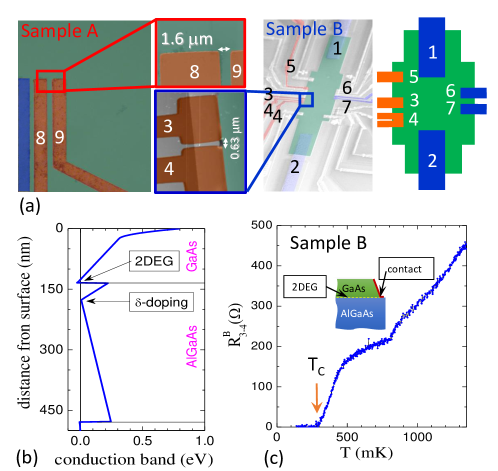
Here we report induced superconductivity in two devices from different wafers, sample A has long ( m) contacts separated by m of 2DEG, for sample B contacts are formed to the edge of a mesa with m separation. Details of device fabrication are described in Methods. When cooled down to 4 K in the dark both samples show resistance in excess of M. After illumination with red light emitting diode (LED) a 2DEG is formed and 2-terminal resistance drops to . As shown in Fig. 1d sample resistance gradually decreases upon cooldown from 4 K to the base temperature and the S-2DEG-S junctions becomes superconducting at K.
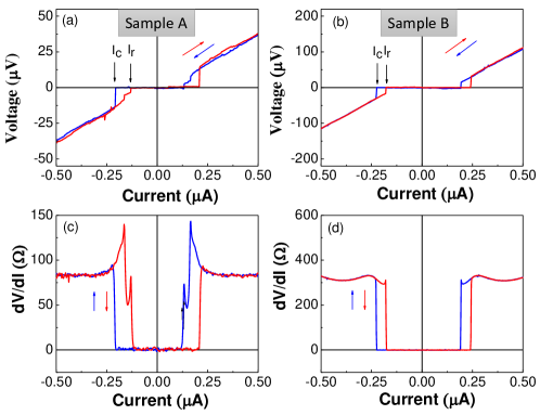
Voltage-current characteristics for two S-2DEG-S junctions (between 8-9 for sample A and between 3-4 for sample B) are shown in Fig. 2. Both samples show zero resistance state at small currents with abrupt switching into resistive state at critical currents A and A for samples A and B respectively. characteristics are hysteretic most likely due to the Joule heating in the normal state.
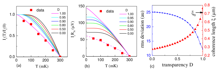
The most attractive property of a high mobility 2DEG is large mean free path , with m and the BCS coherence length m for sample B. Here is the Fermi velocity, is a 2D gas density, is an effective mass, and eV is the induced superconducting gap. Evolution of with is shown Fig. 3a. Experimentally obtained -dependence of is best described by the Kulik-Omelyanchuk theory for ballistic junctions ()Kulik and Omel’yanchuk (1977), the blue curve on Fig. 3b. For comparison we also plot dependence for the dirty limit Kulik and Omel’yanchuk (1975), which exhibits characteristic saturation of at low temperatures.
In short ballistic junctions the product does not depend on the junction length . For this product is reduced by a factor Bagwell (1992). The measured V for sample B is in a good agreement with an estimate V. For sample A the V while the estimated product is V. The reduction is consistent with the geometry of sample A, where a region of the 2DEG with induced superconductivity is shunted by a large region of a 2DEG in a normal state.
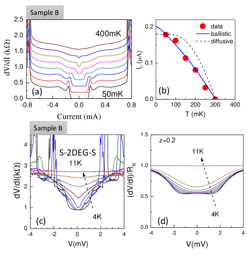
Transparency of superconducting contacts can be estimated from the suppression of the superconducting gap in the S-2DEG-S junction between 3-4 in sample B. In one-dimensional junctions the induced gap depends on the broadening of Andreev levels within the semiconductorSau et al. (2012) , where we introduce contacts transparencies and . We assume for simplicity that , where is a interface barrier strength introduced in Blonder et al. (1982), and Bagwell’s effective channel length . Using NbN superconducting gap (NbN is a strong-coupling superconductor, K) we obtain . This value is consistent with the fit of the vs dependence with as a free parameter, see Supplementary Material for details. Similar values of can be estimated from the analysis of the shape of characteristics at elevated temperatures, as shown in Fig. 3. At Andreev reflection at S-2DEG interfaces results in an excess current flowing through the junction for voltage biases within the superconducting gap and corresponding reduction of a differential resistance by a factor of 2. In the presence of a tunneling barrier normal reflection competes with Andreev reflection and reduced excess current near zero bias, resulting in a peak in differential resistance. Within the BTK theoryBlonder et al. (1982) a flat within , observed in our experiments, is expected only for contacts with very high transparency . For larger a peak at low biases is expected (see Supplementary Material). Several features of the experimental need to be mentioned. First, we observe several sharp peaks in the resistance at high biases (around 2 mV and 4 mV for K). Similar sharp resonances has been observed previously Gao et al. (1994), where authors attributed their appearance to the formation of Fabry-Pérot resonances between superconducting contacts. In our devices the superconducting region is shunted by a low resistance () 2DEG, thus appearance of k resonances cannot be explained by resonant electron trapping between contacts. These resonances are also observed in characteristics of a single S-2DEG interface (measured in the S-2DEG-N configuration between contacts 3-6, see Supplementary Material Fig. S2). Differential resistance does not change substantially across resonances, ruling out transport through a localized state. We speculate that in the contacts where these resonances are observed superconductivity is carried out by quasi-1D channels, and jumps in I/V characteristics are due to flux trapping at high currents. This scenario is consistent with the observation that peaks shift to lower currents at higher fields, see Fig. 4. The second notable feature of our data is reduction of the zero-bias resistance by at low temperatures, while Andreev reflection limits the reduction to the factor of 2. We attribute this reduction to the multiple Andreev reflection between two closely-spaced contacts, for contacts with larger separation ( m) multiple Andreev reflection is suppressed and the reduction of resistance by a factor of 2 is observed, see Supplementary Material Fig. S2.
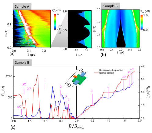
Finally, we present magnetic field dependence of induced superconductivity. The low-field data is shown in Fig. 4(a,b), where black regions correspond to zero differential resistance. Induced superconductivity is suppressed at T in both samples. In sample A a narrow region of a 2DEG with induced superconductivity is confined between large NbN superconducting leads with rigid phases. Perpendicular magnetic field twists the phase in the 2DEG resulting in Fraunhofer-like oscillations of the critical current. In this sample, though, the 2DEG extends beyond the narrow region between the contacts and does not decrease to zero and abrupt jumps in reflect multiple flux jumps. The period of oscillations is mT which corresponds to an area of 4.1 m2, much smaller than the area of the 2DEG between the contacts ( m2). This observation is consistent with the reduced product measured for this sample as discussed above. In sample B contacts are fabricated along the edge of the mesa and 2D gas is not enclosed between the contacts. Consequently, is a smooth function of .
Competition between superconductivity and chiral quantum Hall edge states is shown in Fig. 4c, where resistance is measured in a 3-terminal configuration over a wide range of magnetic fields. Simple Landauer-Buttiker model of edge states predicts zero resistance for negative and quantized Hall resistance for positive field direction for IQHE and FQHE states, which is clearly seen in a sample with all normal ohmic contacts (red curve). When a superconducting contact serves as a current injector (blue curve), integer and fractional and 3/5 states are well developed for , while the same states are not quantized at proper QHE values for . If we assume that current injection via a superconducting contact results in an extra voltage offset at the contact , the measured voltage will be reduces by . The magenta bars for indicate corrected resistance for V. While this offset may explain the measured values for fractional states, a twice smaller is needed to reconcile the resistance at . Note that induced gap is smaller at higher . At low fields states , 4 and 5 have resistance minima for indicating partial equilibration of chiral edge currents with the superconducting contact, while resistance near has a maximum. Zero resistance at and large resistance at are in contrast to the theoretical prediction that state should be stronger coupled to a superconducting contact than Fisher (1994).
Methods
The GaAs/AlGaAs inverted heterojunctions were grown by molecular beam epitaxy (MBE) on semi-insulating (100) GaAs substrates with the heterointerface placed 130 nm below the surface and -doping layer 30-40 nm below the GaAs/AlGaAs interface. Samples were fabricated from two wafers with density and mobility cm-2, Vs/cm2 (sample A) and cm-2, Vs/cm2 (sample B). Superconducting contacts were defined by standard electron beam lithography. First, a 120 nm - deep trench was created by wet etching. Next, samples were dipped into HCl:H2O solution for 2 s and loaded into a thermal evaporation chamber, where Ti/AuGe (5nm/50nm) was deposited. Finally, 70 nm of NbN was deposited by DC magnetron sputtering in Ar/N2 () plasma at a total pressure of 2 mTorr. The deposition conditions were optimized for producing high quality NbN films ( K and Tesla) with minimal strainGlowacka et al. (2014). The contacts were annealed at C for 10 min in a forming gas. The measurements were performed in a dilution refrigerator with base temperature mK, high temperature data was obtained in a variable temperature 3He system. Samples were illuminated with red LED at 4 K in order to form a 2D gas, 2-terminal resistance drops from M before illumination to after illumination.
Acknowledgements
The work at Purdue was supported by the National Science Foundation grant DMR-1307247 (Z.W. and L.P.R.), by the Purdue Center for Topological Materials (Z.W.), and by the U.S. Department of Energy, Office of Basic Energy Sciences, Division of Materials Sciences and Engineering under Awards DE-SC0008630 (A.K.) and DE-SC0006671 (M.J.M.). The work at Princeton was funded by the Gordon and Betty Moore Foundation through Grant GBMF 4420, and by the National Science Foundation MRSEC at the Princeton Center for Complex Materials.
Authors contribution
L.P.R. and M.J.M conceived the experiments, Z.W. fabricated samples, Z.W. and L.P.R performed experiments, Z.W. and L.P.R wrote the manuscript with comments from M.J.M, L.N.P. and K.W.W. designed and grew wafers, A.K. contributed to the fabrication and low temperature experiments.
Additional information
Supplementary information is available in the online version of the paper. Correspondence
should be addressed to L.P.R.
Competing financial interests
The authors declare no competing financial interests.
References
- Clark et al. (1980) T. D. Clark, R. J. Prance, and A. D. C. Grassie, “Feasibility of hybrid Josephson field effect transistors,” Journal of Applied Physics 51, 2736–2743 (1980).
- Takayanagi and Kawakami (1985) Hideaki Takayanagi and Tsuyoshi Kawakami, “Superconducting proximity effect in the native inversion layer on InAs,” Phys. Rev. Lett. 54, 2449–2452 (1985).
- Akazaki et al. (1996) Tatsushi Akazaki, Hideaki Takayanagi, Junsaku Nitta, and Takatomo Enoki, “A Josephson field effect transistor using an InAs inserted channel In0.52Al0.48As/In0.53Ga0.47As inverted modulation-doped structure,” Applied Physics Letters 68, 418–420 (1996).
- Heersche et al. (2007) Hubert B. Heersche, Pablo Jarillo-Herrero, Jeroen B. Oostinga, Lieven M. K. Vandersypen, and Alberto F. Morpurgo, “Bipolar supercurrent in graphene,” Nature 446, 56–59 (2007).
- Sacepe et al. (2011) Benjamin Sacepe, Jeroen B. Oostinga, Jian Li, Alberto Ubaldini, Nuno J.G. Couto, Enrico Giannini, and Alberto F. Morpurgo, “Gate-tuned normal and superconducting transport at the surface of a topological insulator,” Nat. Commun. 2, 575 (2011).
- Williams et al. (2012) J. R. Williams, A. J. Bestwick, P. Gallagher, Seung Sae Hong, Y. Cui, Andrew S. Bleich, J. G. Analytis, I. R. Fisher, and D. Goldhaber-Gordon, “Unconventional Josephson effect in hybrid superconductor-topological insulator devices,” Physical Review Letters 109, 056803 (2012).
- Veldhorst et al. (2012) M. Veldhorst, M. Snelder, M. Hoek, T. Gang, V. K. Guduru, X. L. Wang, U. Zeitler, W. G. van der Wiel, A. A. Golubov, H. Hilgenkamp, and A. Brinkman, “Josephson supercurrent through a topological insulator surface state,” Nat. Mater. 11, 1–4 (2012).
- Qu et al. (2012) Fanming Qu, Fan Yang, Jie Shen, Yue Ding, Jun Chen, Zhongqing Ji, Guangtong Liu, Jie Fan, Xiunian Jing, Changli Yang, and Li Lu, “Strong superconducting proximity effect in Pb-Bi2Te3 hybrid structures,” Sci. Rep. 2, 339 (2012).
- Doh et al. (2005) Yong-Joo Doh, Jorden A. van Dam, Aarnoud L. Roest, Erik P. A. M. Bakkers, Leo P. Kouwenhoven, and Silvano De Franceschi, “Tunable supercurrent through semiconductor nanowires,” Science 309, 272–275 (2005).
- Jarillo-Herrero et al. (2006) Pablo Jarillo-Herrero, Jorden A. van Dam, and Leo P. Kouwenhoven, “Quantum supercurrent transistors in carbon nanotubes,” Nature 439, 953–956 (2006).
- Xiang et al. (2006) Jie Xiang, A. Vidan, M. Tinkham, R.M. Westervelt, and C.M. Lieber, “Ge/Si nanowire mesoscopic Josephson junctions,” Nature Nanotechnology 1, 208 – 213 (2006).
- Hart et al. (2014) Sean Hart, Hechen Ren, Timo Wagner, Philipp Leubner, Mathias Muhlbauer, Christoph Brune, Hartmut Buhmann, Laurens W. Molenkamp, and Amir Yacoby, “Induced superconductivity in the quantum spin hall edge,” Nat. Phys 10, 638–643 (2014).
- Yu et al. (2014) Wenlong Yu, Yuxuan Jiang, Chao Huan, Xunchi Chen, Zhigang Jiang, Samuel D. Hawkins, John F. Klem, and Wei Pan, “Superconducting proximity effect in inverted InAs/GaSb quantum well structures with Ta electrodes,” (2014), arXiv:1402.7282 .
- Rokhinson et al. (2012) Leonid P. Rokhinson, Xinyu Liu, and Jacek K. Furdyna, “The fractional a.c. Josephson effect in a semiconductor-superconductor nanowire as a signature of Majorana particles,” Nat. Phys. 8, 795 – 799 (2012).
- Mourik et al. (2012) V. Mourik, K. Zuo, S. M. Frolov, S. R. Plissard, E. P. A. M. Bakkers, and L. P. Kouwenhoven, “Signatures of Majorana fermions in hybrid superconductor-semiconductor nanowire devices,” Science 336, 1003 – 1007 (2012).
- Fu and Kane (2009) Liang Fu and C. L. Kane, “Josephson current and noise at a superconductor/quantum-spin-Hall-insulator/superconductor junction,” Phys. Rev. B 79, 161408 (2009).
- Lutchyn et al. (2010) Roman M. Lutchyn, Jay D. Sau, and S. Das Sarma, “Majorana fermions and a topological phase transition in semiconductor-superconductor heterostructures,” Phys. Rev. Lett. 105, 077001 (2010).
- Alicea (2010) Jason Alicea, “Majorana fermions in a tunable semiconductor device,” Phys. Rev. B 81, 125318 (2010).
- Clarke et al. (2012) David J. Clarke, Jason Alicea, and Kirill Shtengel, “Exotic non-Abelian anyons from conventional fractional quantum Hall states,” Nat. Commun. 4, 1348 (2012).
- Mong et al. (2014) Roger S. K. Mong, David J. Clarke, Jason Alicea, Netanel H. Lindner, Paul Fendley, Chetan Nayak, Yuval Oreg, Ady Stern, Erez Berg, Kirill Shtengel, and Matthew P. A. Fisher, “Universal topological quantum computation from a superconductor-Abelian quantum hall heterostructure,” Phys. Rev. X 4, 011036 (2014).
- Zuo et al. (2014) Zheng-Wei Zuo, L. Sheng, and D.Y. Xing, “Crossed Andreev reflections in superconductor and fractional quantum Hall liquids hybrid system,” Solid State Communications 184, 17 – 20 (2014).
- Zyuzin (1994) A. Yu. Zyuzin, “Superconductor-normal-metal-superconductor junction in a strong magnetic field,” Phys. Rev. B 50, 323–329 (1994).
- Fisher (1994) Matthew P. A. Fisher, “Cooper-pair tunneling into a quantum Hall fluid,” Phys. Rev. B 49, 14550–14553 (1994).
- Hoppe et al. (2000) H. Hoppe, U. Zülicke, and Gerd Schön, “Andreev reflection in strong magnetic fields,” Phys. Rev. Lett. 84, 1804–1807 (2000).
- Kim et al. (2004) Eun-Ah Kim, Smitha Vishveshwara, and Eduardo Fradkin, “Cooper-pair tunneling in junctions of singlet quantum Hall states and superconductors,” Phys. Rev. Lett. 93, 266803 (2004).
- Giazotto et al. (2005) F. Giazotto, M. Governale, U. Zülicke, and F. Beltram, “Andreev reflection and cyclotron motion at superconductor/normal-metal interfaces,” Phys. Rev. B 72, 054518 (2005).
- van Ostaay et al. (2011) J. A. M. van Ostaay, A. R. Akhmerov, and C. W. J. Beenakker, “Spin-triplet supercurrent carried by quantum Hall edge states through a Josephson junction,” Phys. Rev. B 83, 195441 (2011).
- Lenssen et al. (1993) K-M. H. Lenssen, M. Matters, C. J. P. M. Harmans, J. E. Mooij, M. R. Leys, W. van der Vleuten, and J. H. Wolter, “Andreev reflection at superconducting contacts to GaAs/AlGaAs heterostructures,” Applied Physics Letters 63, 2079–2081 (1993).
- Moore and Williams (1999) T. D. Moore and D. A. Williams, “Andreev reflection at high magnetic fields,” Phys. Rev. B 59, 7308–7311 (1999).
- Verevkin et al. (1999) A.A. Verevkin, N.G. Ptitsina, K.V. Smirnov, B.M. Voronov, G.N. Gol’tsman, E.M. Gershenson, and K.S. Yngvesson, “Multiple Andreev reflection in hybrid AlGaAs GaAs structures with superconducting NbN contacts,” semiconductors 33, 551–554 (1999).
- Takayanagi et al. (2002) Hideaki Takayanagi, Tatsushi Akazaki, Minoru Kawamura, Yuichi Harada, and Junsaku Nitta, “Superconducting junctions using AlGaAs/GaAs heterostructures with high hc2 NbN electrodes,” Physica E 4, 922 – 926 (2002).
- Kutchinsky et al. (2001) Jonatan Kutchinsky, Rafael Taboryski, Claus Birger Sørensen, Jørn Bindslev Hansen, and Poul Erik Lindelof, “Experimental investigation of supercurrent enhancement in s-n-s junctions by non-equilibrium injection into supercurrent-carrying bound Andreev states,” Physica C: Superconductivity 352, 4 – 10 (2001).
- Marsh et al. (1994) A.M. Marsh, D. A. Williams, and H. Ahmed, “Supercurrent transport through a high-mobility two-dimensional electron gas,” Phys. Rev. B 50, 8118–8121 (1994).
- Snider et al. (1990) G. L. Snider, I.-H. Tan, and E. L. Hu, “Electron states in mesa-etched one-dimensional quantum well wires,” J. Appl. Phys. 68, 2849 (1990).
- Kulik and Omel’yanchuk (1977) I.O. Kulik and A.N. Omel’yanchuk, “Properties of superconducting microbridges in the pure limit.” Sov. J. Low Temp. Phys. 3, 459 – 461 (1977).
- Kulik and Omel’yanchuk (1975) I.O. Kulik and A.N. Omel’yanchuk, “Microscopic theory of the Josephson effect in superconducting bridges,” Pisma v ZETF 21, 216 – 19 (1975).
- Bagwell (1992) Philip F. Bagwell, “Suppression of the Josephson current through a narrow, mesoscopic, semiconductor channel by a single impurity,” Phys. Rev. B 46, 12573–12586 (1992).
- Blonder et al. (1982) G. E. Blonder, M. Tinkham, and T. M. Klapwijk, “Transition from metallic to tunneling regimes in superconducting microconstrictions: Excess current, charge imbalance, and supercurrent conversion,” Phys. Rev. B 25, 4515–4532 (1982).
- Sau et al. (2012) J. D. Sau, S. Tewari, and S. Das Sarma, “Experimental and materials considerations for the topological superconducting state in electron and hole doped semiconductors: searching for non-Abelian Majorana modes in 1d nanowires and 2d heterostructures,” Phys. Rev. B 85, 064512 (2012).
- Gao et al. (1994) JR Gao, JP Heida, B.J. van Wees, T.M. Klapwijk, G. Borghs, and C.T. Foxon, “Superconductors coupled with a two-dimensional electron gas in GaAs/AlGaAs and InAs/AlGaSb heterostructures,” Surface Science 305, 470–475 (1994).
- Glowacka et al. (2014) D. M. Glowacka, D. J. Goldie, S. Withington, H. Muhammad, G. Yassin, and B. K. Tan, “Development of a NbN deposition process for superconducting quantum sensors,” (2014), arXiv:1401.2292 .
- Haberkorn et al. (1978) W. Haberkorn, H. Knauer, and J. Richter, “A theoretical study of the current-phase relation in Josephson contacts,” Physics Status Solidi 47, K161–K164 (1978).
- Neurohr et al. (1996) K. Neurohr, A. A. Golubov, Th. Klocke, J. Kaufmann, Th. Schäpers, J. Appenzeller, D. Uhlisch, A. V. Ustinov, M. Hollfelder, H. Lüth, and A. I. Braginski, “Properties of lateral Nb contacts to a two-dimensional electron gas in an In0.77Ga0.23As/InP heterostructure,” Phys. Rev. B 54, 17018–17028 (1996).
Supplementary Materials
Superconductivity in ballistic junctions in high mobility two dimensional electron gas in GaAs heterostructures.
Zhong Wan, Michael Manfra, Loren Pfeiffer, Ken West, and Leonid P. Rokhinson
I Temperature dependence of the critical current
Haberkorn et al. Haberkorn et al. (1978) generalized Kulik-Omelyanchuk current-phase relationsKulik and Omel’yanchuk (1977, 1975) to the case of arbitrary transparency of a tunnel barrier inserted into the Josephson junction by directly solving Gor’kov’s equations. They obtain the following current-phase relation:
| (S1) |
where is the BCS gap. For this equation interpolated between diffusive () and ballistic () junctions. Critical current can be found as . We introduce coefficient to account for the reduction of the critical current due to the finite length of the junction , Bagwell (1992). The best fit of the experimental dependence assuming both and as free parameters is obtained for and , see Fig. S1(a,b). For the contact spacing m this corresponds to m, consistent with the BCS coherence length m. Transparency can be related to the dimensionless barrier strength introduced in the Blonder-Tinkham-Klapwijk (BTK) theoryBlonder et al. (1982), , and the fit sets the upper limit on , . The quality of the fit parameters can be assessed from Fig. S1(c), where rms error for the best fit with a fixed and as a free parameter is plotted for different . The rms deviation has a clear global minimum at . Note that the coherence length for , obtained from the fitting parameter , becomes smaller than the estimated .
II Analysis of excess current above the induced superconductivity gap
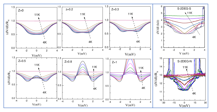
Transparency of the superconductor-semiconductor interface can be estimated from the shape of the characteristic, where competition between Andreev and normal reflections results in a peak in differential resistance when a tunneling barrier is present at the superconductor-semiconductor interface (transmission ). Differential resistance for different temperatures can be calculated using Blonder-Tinkham-Klapwijk (BTK) theoryBlonder et al. (1982):
| (S2) |
where is the Fermi Dirac function and and are energy-dependent Andreev and normal reflection coefficients, respectively. Both coefficients depend on the gap of NbN with K and the interface barrier strength . In Fig. S2 we plot differential resistance for different values of . At low for the barrier is transparent () and all incident electrons are Andreev reflected, which leads to the a reduction of differential resistance by a factor of 2 within the energy gap . When is finite, part of the incident electrons undergoes normal reflection which results in the increase of the resistance within the gap.
The exact shape of experimental curves differ from the shape predicted by the BKT theory, the most important deviation being sharp minima near observed at close to as compared to a much smoother BKT dependence. To account for a similar sharpening of a zero-bias peak in less transparent contacts () it has been assumed that a thin normal region is formed between NbN contacts and a 2DEGNeurohr et al. (1996). This more elaborate theory introduces two more fitting parameters for the superconducting-normal and normal-2DEG interfaces, but does not change the main qualitative prediction of a simpler BTK theory: appearance of a peak near for in characteristics.
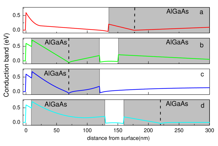
III Comparison between conventional heterostructures and inverted single interface heterostructure
Comparison between conventional heterostructures and inverted heterostructures used in this work is shown in Fig. S3. In conventional quantum well (b,d) and single interface heterostructures AlGaAs barrier between 2D gas and the surface adds 0.3 eV to the Schottky barrier if contacts are defused from the surface. For side contacts inverted single heterointerface (a) increases the exposed GaAs cross section for Cooper pair injection.