Why graphene growth is very different on the C face than on the Si face of SiC: Insights from surface equilibria and the (33)-3C-SiC() reconstruction
Abstract
We address the stability of the surface phases that occur on the C-side of 3C-SiC() at the onset of graphene formation. In this growth range, experimental reports reveal a coexistence of several surface phases. This coexistence can be explained by a Si-rich model for the unknown (33) reconstruction, the known (22)C adatom phase, and the graphene covered (22)C phase. By constructing an ab initio surface phase diagram using a van der Waals corrected density functional, we show that the formation of a well defined interface structure like the “buffer-layer” on the Si side is blocked by Si-rich surface reconstructions.
pacs:
61.48.Gh, 68.35.B, 68.35.Md, 68.65.PGraphene grown on silicon carbide (SiC) is one of the most promising material combinations for future graphene applications.Berger et al. (2006); Emtsev et al. (2009); Lin et al. (2011); Hertel et al. (2012); de Heer (2011); Guo et al. (2013) On SiC, graphene growth is achieved by thermal decomposition of the substrate.Van Bommel et al. (1975); Forbeaux et al. (2000); Berger et al. (2004) The electronic properties of few-layer graphene films grown on the C-side of the polar SiC surface are similar to those of an isolated monolayer graphene film with very high electron mobilities.Hass et al. (2008a); Sprinkle et al. (2009); Berger et al. (2010) However, controlling the layer thickness of the graphene films remains a challenge.Mathieu et al. (2011) While some groups report the successful growth of large-scale monolayer graphene Hu et al. (2012); Ruan et al. (2012), other reports suggest that the pure monolayer growth regime is difficult to achieve on the C face of SiC. Mathieu et al. (2011) This is very different from the Si side, where nearly perfect, monolayer graphene films can be grown over large areas.Emtsev et al. (2009); de Heer (2011) Investigating the relative phase stability of the competing surface phases in the thermodynamic range of graphitisation is an important step for a better understanding of graphene growth.
For epitaxial graphene films on the Si-side of 3C-SiC(111), we have recently shown by ab initio atomistic thermodynamics that individual phases, the ()-R30∘ zero layer and monolayer graphene (ZLG and MLG) can form as near equilibrium phases under certain external conditions (represented by the C and Si chemical potentials that are controlled by temperature and background gas pressure in experiment, see also Eq. (1) below).Nemec et al. (2013) What is not a priori clear is whether on the C face of SiC, graphene films can also be thermodynamically stable. To address this question, atomistic models are required for the different competing phases, in particular for the C rich conditions close to the graphitization regime.
We here present first-principles evidence that the formation of monolayer graphene films on the C face is hindered by stable Si rich phases. This is a major and unexpected difference to the case of the Si face, where the formation of a C-rich, so-called “buffer layer” phase is actually aided by the formation of heterogeneous C-Si bonds. To shed light on the phase mixture at the graphitisation limit on the C face, we use a possible model of the unknown (33) reconstruction. The central feature of this model is a capping layer of Si atoms, minimizing dangling bonds in the same way as the known Si-rich (33) phase on the Si face of SiC.Starke et al. (1998); Schardt et al. (2000)
On the C-side, a series of different surface structures have been observed during annealing.Van Bommel et al. (1975); Starke (1997); Hoster et al. (1997); Li and Tsong (1996); Bernhardt et al. (1999a); Seubert et al. (2000); Magaud et al. (2009); Hiebel et al. (2009); Starke and Riedl (2009); Hiebel et al. (2012) Graphene growth starts either with a Si rich (22) phase in an Si rich environmentBernhardt et al. (1999a); Li and Tsong (1996) or with an oxidic () reconstruction.Bernhardt et al. (1999b); Li and Tsong (1996) In the absence of a Si background like disilane, a (11) phase is observed, which exhibits the periodicity of bulk SiC underneath a disordered oxidic layer.Starke (1997) Continued heating leads to a (33) phase. Using qualitative low-energy electron diffraction (LEED), Bernhardt et al. Bernhardt et al. (1999a) showed that the (33) reconstructions originating from different starting structures and environments are equivalent.Bernhardt et al. (1999a) Further annealing leads to a (22) Si ad-atom phase, referred to as (22) (notation taken from Bernhardt et al. (1999a)). Just before graphene forms on the surface, a coexistence of the two surface phases, the (33) as well as the (22), is observed. Bernhardt et al. (1999a); Veuillen et al. (2010) In addition, different groups reported strong experimental evidence that both reconstructions persist underneath the graphene films with the (33) phase gradually fading, but never disappearing.Hass et al. (2007); Hiebel et al. (2008); Emtsev et al. (2008); Hass et al. (2008b); Starke and Riedl (2009); Veuillen et al. (2010); Hiebel et al. (2012); Moreau et al. (2013) While the atomic structure of the (22) reconstruction was resolved by quantitative LEED Seubert et al. (2000), the (33) reconstruction and the graphene/ SiC interface remain a puzzle.
In the past, several structural models were suggested for the (33) phase on the C face.Li and Tsong (1996); Hoster et al. (1997); Hiebel et al. (2012); Deretzis and La Magna (2013) We here summarise its experimentally observed characteristics. Its stoichiometry was found to be Si-rich by Auger electron spectroscopy (AES).Hoster et al. (1997); Bernhardt et al. (1999a) The corresponding filled state scanning tunneling microscope (STM) image is consistent with three adatoms residing at the same height.Deretzis and La Magna (2013); Hiebel et al. (2012) Scanning tunnelling spectroscopy shows a semiconducting surface with a eV band gap.Hiebel et al. (2009)
For the graphene/SiC interfaces on the C-side two different scenarios have been invoked. a) The first carbon layer is strongly bound to the substrate.Varchon et al. (2007); Mathieu et al. (2011); Srivastava et al. (2012) In this scenario, the Si sublimation rate during graphene growth is controlled by either working in an inert gas atmosphere Emtsev et al. (2009), by using a confined geometry Hass et al. (2008b), or by providing an external Si gas phase Srivastava et al. (2012); Forbeaux et al. (2000) for example disilane. It is not clear, however, if the different groups observe the same structures. Based on their LEED data, Srivastava et al. Srivastava et al. (2012) proposed a -R SiC substrate with a (88) carbon mesh rotated by with respect to the substrate (’-R’).Srivastava et al. (2012) The detailed atomic structure of this interface is not known.He et al. (2013) b) For samples prepared under ultra-high vacuum conditions, the first carbon layer is weakly bound to the substrate, showing the characteristic behavior of the -band at the -point of the Brillouin zone. Here an inhomogeneous interface is present since the (33) as well as a (22) reconstruction is observed underneath the graphene layers.Hiebel et al. (2008); Emtsev et al. (2008); Starke and Riedl (2009) A recent study on graphene grown by molecular beam epitaxy (MBE) on the C-side exhibited the same structural characteristics as graphene grown by high-temperature annealing.Moreau et al. (2013) This is a strong indication that indeed the (22) as well as the (33) reconstruction prevails below the graphene films.
To our knowledge, the different (33) models suggested in the literature and likewise the remaining phases including the graphene/SiC interfaces have not yet been placed in the context of a surface phase diagram. We employ density-functional theory (DFT) using the FHI-aims all-electron code Blum et al. (2009); Havu et al. (2009) with the ELPA eigensolver library.Auckenthaler et al. (2011); Marek et al. (2014) We use the van der Waals (vdW) corrected Tkatchenko and Scheffler (2009) Perdew-Burke-Enzerhof (PBE) generalised gradient approximationPerdew et al. (1997) (PBE+vdW) and the Heyd-Scuseria-Ernzerhof hybrid functional (HSE06+vdW) Krukau et al. (2006); Tkatchenko and Scheffler (2009) for the exchange correlation functional. Unless otherwise noted the calculations are non-spinpolarised. Technical parameters and bulk lattice constants are listed in the supplemental material (SM)sup . In contrast to hexagonal polytypes, at the surface of 3C-SiC only one type of stacking order is present Starke (1997). Although the growth process La Via et al. (2014) and the electronic structure Pankratov et al. (2012) differ among polytypes, the surface reconstruction does not seem to be affected Furthmüller et al. (1998); Schardt et al. (2000); Pankratov et al. (2012).
A good indicator for finding the most likely (33) reconstruction or interface structures is a comparison of the respective surface free energies as formulated in the ab initio atomistic thermodynamics approach.Weinert and M. (1986); Scheffler (1988); Scheffler and Dabrowski (1988); Reuter and Scheffler (2001); Reuter et al. (2005) We neglect vibrational and configurational entropy contributions to the free energy, although in the coexistence region they might lead to small shifts. In the limit of sufficiently thick slabs, the surface energy of a two-dimensional periodic SiC slab with a C face and a Si face is given as
| (1) |
and denote the number of Si and C atoms in the slab, respectively. and refer to the chemical potentials of Si and C. The stability of the SiC bulk dictates where is the total energy of a bulk SiC unit cell. All surface energies are given in eV per area () of a (11) SiC unit cell. The letter denotes total energies for a given atomic geometry throughout this work. The chemical potential limits of the C and Si reservoirs are fixed by the requirement that the underlying SiC bulk is stable against decomposition Nemec et al. (2013), leading to: . Because of the close competition between the diamond and graphite structure for C Berman and Simon (1955); Yin and Cohen (1984); Yu et al. (2014), we include both limiting phases in our analysis.
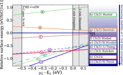
The surface energies of the (22) surface model by Seubert et al. and the different models for the SiC-(33) reconstruction are shown as a function of in Fig. 1. The structure with the lowest energy for a given corresponds to the most stable phase. We here briefly discuss the alternative surface phases of the SiC C face (for more details see SM sup ). Hoster, Kulakov, and Bullemer suggested a geometric configuration for the (33) reconstruction on the basis of STM measurements without specifying the chemical composition.Hoster et al. (1997) Highest in surface energy is the variation suggested by Hiebel et al. Hiebel et al. (2012) labeled h, followed by a carbon rich composition suggested by Deretzis and La Magna Deretzis and La Magna (2013) labeled g. We added a modification with all adatoms chosen to be Si, labeled e. Of all the Hoster-type models that we tested, this is the most stable chemical composition. Hiebel et al. suggested a new model, labeled f. Hiebel et al. (2012) Li and Tsong proposed a tetrahedrally shaped cluster as reconstruction.Li and Tsong (1996) They suggested a Si and C rich configuration. We tested both configurations and included an additional Si tetrahedron (for details see SM sup ). Here, we include only the most stable cluster formed by 4 Si atoms, labeled d. Finally, we added a model originally proposed as a Si rich structure for the 6H-SiC()-(33) reconstruction by Kulakov, Henn, and Bullemer Kulakov et al. (1996), labeled c. To summarise Fig. 1, all the alternative models we tested are too high in energy at the graphite line to coexist with the (22) adatom model.
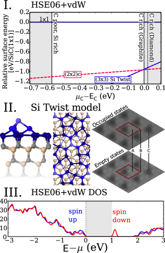
We next show that a conceptual model for the (33) reconstruction based on a Si-rich termination performs much better at explaining the various surface characteristics. To create a plausible termination, we base our model on the Si twist model Starke et al. (1998); Schardt et al. (2000), known from the 3C-SiC()–(33) reconstruction. In Fig. 2 (II) its geometry is shown in a side view and from atop. The top bulk C layer is covered by a Si adlayer forming heterogeneous Si-C bonds. Three Si adatoms form a triangle twisted by with respect to the top SiC layer. In comparison, the twist angle on the Si side amounts to . The topmost Si adatom is positioned on top of the triangle. In the surface diagram (Fig. 1), this phase has the lowest energy of all previously proposed (33) models. Its formation energy crosses that of the (22) phase just at the C rich limit (graphite) of the chemical potential. To coexist with the (22) phase and to be present at the onset of graphite formation, the (33) phase has to cross the graphite line very close to the crossing point between the graphite line and the (22) phase. The Si twist model shown in Fig. 2 satisfies this condition.
In agreement with the AES experiments our model is Si-rich. We also compared the surface energetics of the coexisting phases (22) and the Si twist model using the higher level HSE06+vdW hybrid functional with fully relaxed structures and unit cells, shown in Fig. 2 (I). As can be seen, the phase coexistence does not depend on the chosen functional. However, to distinguish between a phase coexistence or a close competition between the two phases, the inclusion of entropy terms would be the next step.Feibelman and Alavi (2004)
In Fig. 2 (III), we show the spin-polarised electronic density of states (DOS) for the spin down (in red) and spin up (in blue) channel. While the spin down surface state gives rise to a peak in the band gap above the Fermi-level, the spin up surface state is in resonance with the SiC bulk states. The DOS clearly demonstrates that the surface is semiconducting in agreement with experiment, featuring a band gap of eV. Thus, the conceptual Si twist model - inspired by the Si side - appears to satisfy the existing experimental constraints well.
Furthermore, our simulated STM images Fig. 2 (II) reproduce the measured height modulation,Hiebel et al. (2012) but the experimentally observed difference in intensity between occupied and empty state images is not captured by our simulated images. The disagreement in the STM images might be an indication that a different structure is observed in the STM measurements. We started an exhaustive structure search Kloppenburg et al. (2014) to find a surface model that is even lower in energy than the Si twist model and that reproduces all experimental observations, including the STM images. However, if an alternative model were to be found, its surface energy would have to be close to the Si twist model at the graphite line to still coexist with the (22) phase. As a result, it would very likely coexist with the Si twist model.
In the following we use the Si twist model as a representative model to shed light on the SiC-graphene interface on the C face. In particular, we will make a simple qualitative argument why the C-rich ZLG interface, critical towards MLG formation on the Si face, does not form. Figure 3 shows the PBE+vdW surface energies of four different interface structures, the (22) surface phase and the proposed (33) Si twist model.
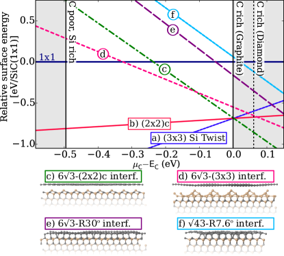
As a first step we constructed an interface structure similar to the ZLG phase known from the Si face - a 6 -R30∘-interface, labeled e in Fig. 3. This structure crosses the graphite line eV above the crossing point of the (33) Si twist model, rendering it unstable. As a second structure, we included a purely C based model of the -R 7.6∘-interface, labeled f in the surface phase diagram of Fig. 3. In our calculations, this structure is even higher in energy than the -R30∘-interface.
The 6 -R30∘- and -R 7.6∘-interface are models of a strongly bound interface. Since the Gibbs energy of formation for SiC is quite large ( eV in experiment Kleykamp (1998), eV in DFT-PBE+vdW and eV in DFT-HSE06+vdW), the formation of SiC bonds is favorable. This explains why the (22) and (33) Si twist model are more stable, because they contain a large number of Si-C bonds. Conversely, the -R30∘- and the -R 7.6∘-interface are made up of energetically less favorable C-C bonds, which increases the surface energy considerably.
For the weakly bound interface a (22) and (33) LEED pattern was observed underneath graphene Hiebel et al. (2008); Emtsev et al. (2008); Starke and Riedl (2009). A typical feature of the LEED structure is a ring like pattern originating from the rotational disorder of graphene films grown on the C face.Hass et al. (2006, 2008a); Hiebel et al. (2008); Veuillen et al. (2010); Hiebel et al. (2008) To model the interface, we limited our study to a 30∘ rotation between the substrate and the graphene film. This choice was motivated by the LEED study of Hass et al.Hass et al. (2008a), who showed that graphene sheets on the C face appear mainly with a 30∘ and a rotation. A 30∘ rotation has also be seen in STM measurements for the graphene covered (22) and (33) phases Hiebel et al. (2008), from here on called (22) and (33). We therefore chose a () SiC supercell covered by a graphene cell rotated by 30∘ with respect to the substrate.
The (22)-interface covers 27 unit cells of the (22) reconstruction (labeled c in Fig. 3). It crosses the (22) reconstruction just to the right of the graphite limit at a chemical potential of meV and a surface energy of eV. This finding demonstrates that the observed LEED pattern underneath the graphene layer is indeed consistent with the well known (22) reconstruction. Our model of the graphene covered (33) phase consist of the same (1313) graphene supercell, covering 12 units of the (33) Si twist model (labeled d in Fig. 3). The surface energy difference between (22)- and the (33)-interface amounts to eV at the graphite line, favoring the (22)-interface.
To put our results into context, we revisit the growth process. In experiment, growth starts with a clean (33) reconstruction. The sample is annealed until the surface is covered by graphene. At this stage, the (33) reconstruction is the dominant phase underneath graphene.Hiebel et al. (2012) However, a shift from the SiC (33) to the (22) surface reconstruction at the graphene/ SiC interface can be stimulated by an additional annealing step at a temperature below graphitisation (950C∘ - 1000C∘) leaving the graphene layer unaffected.Hiebel et al. (2012) Graphene growth starts at a point where bulk SiC decomposes. The interface is determined by the momentary stoichiometry at which the sublimation stopped - a coexistence of different phases is observed. The final annealing step shifts the chemical potential into a regime in which SiC bulk decomposition stops and the graphene layer does not disintegrate, but the SiC surface at the interface moves closer to local equilibrium, in agreement with the phase diagram in Fig. 3, forming an interface structure between the (22) reconstruction and graphene.
In summary, we shed new light on the central aspects of the thermodynamically stable phases that govern the onset of graphene formation on SiC(). In our view, the main difference between the Si face and the C face is the fact that Si-terminated phases are more stable on the C face due to the formation of heterogeneous Si-C bonds. The Si rich phases are thus stable practically up to the graphite line, allowing the surface to form graphene only at the point where bulk SiC itself is no longer stable. This makes monolayer graphene growth on the C side more difficult than on the Si face.
Acknowledgements.
The authors thank Dr. Fanny Hiebel, Dr. Ulrich Starke, and Renaud Puybaret for fruitful discussions during the preparation of this work. This work was partially supported by the DFG collaborative research project 951 “HIOS”.References
- Berger et al. (2006) C. Berger, Z. Song, X. Li, X. Wu, N. Brown, C. Naud, D. Mayou, T. Li, J. Hass, and A. Marchenkov, Science 312, 1191 (2006).
- Emtsev et al. (2009) K. V. Emtsev, A. Bostwick, K. Horn, J. Jobst, G. L. Kellogg, L. Ley, J. L. McChesney, T. Ohta, S. A. Reshanov, J. Röhrl, E. Rotenberg, A. K. Schmid, D. Waldmann, H. B. Weber, and T. Seyller, Nature Materials 8, 203 (2009).
- Lin et al. (2011) Y. Lin, A. Valdes-Garcia, S. Han, D. Farmer, I. Meric, Y. Sun, Y. Wu, C. Dimitrakopoulos, A. Grill, P. Avouris, et al., Science 332, 1294 (2011).
- Hertel et al. (2012) S. Hertel, D. Waldmann, J. Jobst, A. Albert, M. Albrecht, S. Reshanov, A. Schöner, M. Krieger, and H. B. Weber, Nature Comm. 3, 957 (2012).
- de Heer (2011) W. A. de Heer, MRS Bulletin 36, 632 (2011).
- Guo et al. (2013) Z. Guo, R. Dong, P. S. Chakraborty, N. Lourenco, J. Palmer, Y. Hu, M. Ruan, J. Hankinson, J. Kunc, J. D. Cressler, C. Berger, and W. A. de Heer, Nano Letters 13, 942 (2013).
- Van Bommel et al. (1975) A. J. Van Bommel, J. E. Crombeen, and A. Van Tooren, Surface Science 48, 463 (1975).
- Forbeaux et al. (2000) I. Forbeaux, J.-M. Themlin, A. Charrier, F. Thibaudau, and J.-M. Debever, Applied Surface Science 162 - 163, 406 (2000).
- Berger et al. (2004) C. Berger, Z. Song, T. Li, X. Li, A. Ogbazghi, R. Feng, Z. Dai, A. Marchenkov, E. Conrad, N. Phillip, et al., J. Phys. Chem. B 108, 19912 (2004).
- Hass et al. (2008a) J. Hass, F. Varchon, J. E. Millán-Otoya, M. Sprinkle, N. Sharma, W. A. de Heer, C. Berger, P. N. First, L. Magaud, and E. H. Conrad, Phys. Rev. Lett. 100, 125504 (2008a).
- Sprinkle et al. (2009) M. Sprinkle, D. Siegel, Y. Hu, J. Hicks, A. Tejeda, A. Taleb-Ibrahimi, P. Le Fèvre, F. Bertran, S. Vizzini, H. Enriquez, S. Chiang, P. Soukiassian, C. Berger, W. A. de Heer, A. Lanzara, and E. H. Conrad, Phys. Rev. Lett. 103, 226803 (2009).
- Berger et al. (2010) C. Berger, J.-Y. Veuillen, L. Magaud, P. Mallet, V. Olevano, M. Orlita, P. Plochocka, C. Faugeras, G. Martinez, M. Potemski, et al., Int. J. Nanotechnol. 7, 383 (2010).
- Mathieu et al. (2011) C. Mathieu, N. Barrett, J. Rault, Y. Y. Mi, B. Zhang, W. A. de Heer, C. Berger, E. H. Conrad, and O. Renault, Phys. Rev. B 83, 235436 (2011).
- Hu et al. (2012) Y. Hu, M. Ruan, Z. Guo, R. Dong, J. Palmer, J. Hankinson, C. Berger, and W. A. de Heer, Journal of Physics D: Applied Physics 45, 154010 (2012).
- Ruan et al. (2012) M. Ruan, Y. Hu, Z. Guo, R. Dong, J. Palmer, J. Hankinson, C. Berger, and W. A. de Heer, MRS Bulletin 37, 1138 (2012).
- Nemec et al. (2013) L. Nemec, V. Blum, P. Rinke, and M. Scheffler, Phys. Rev. Lett. 111, 065502 (2013).
- Starke et al. (1998) U. Starke, J. Schardt, J. Bernhardt, M. Franke, K. Reuter, H. Wedler, K. Heinz, J. Furthmüller, P. Käckell, and F. Bechstedt, Phys. Rev. Lett. 80, 758 (1998).
- Schardt et al. (2000) J. Schardt, J. Bernhardt, U. Starke, and K. Heinz, Phys. Rev. B 62, 10335 (2000).
- Starke (1997) U. Starke, physica status solidi (b) 202, 475 (1997).
- Hoster et al. (1997) H. E. Hoster, M. A. Kulakov, and B. Bullemer, Surface Science 382, L658 (1997).
- Li and Tsong (1996) L. Li and I. S. T. Tsong, Surface Science 351, 141 (1996).
- Bernhardt et al. (1999a) J. Bernhardt, M. Nerding, U. Starke, and K. Heinz, Materials Science and Engineering: B 61 – 62, 207 (1999a).
- Seubert et al. (2000) A. Seubert, J. Bernhardt, M. Nerding, U. Starke, and K. Heinz, Surface Science 454 – 456, 45 (2000).
- Magaud et al. (2009) L. Magaud, F. Hiebel, F. Varchon, P. Mallet, and J.-Y. Veuillen, Phys. Rev. B 79, 161405 (2009).
- Hiebel et al. (2009) F. Hiebel, P. Mallet, L. Magaud, and J.-Y. Veuillen, Phys. Rev. B 80, 235429 (2009).
- Starke and Riedl (2009) U. Starke and C. Riedl, Journal of Physics: Condensed Matter 21, 134016 (2009).
- Hiebel et al. (2012) F. Hiebel, L. Magaud, P. Mallet, and J.-Y. Veuillen, Journal of Physics D: Applied Physics 45, 154003 (2012).
- Bernhardt et al. (1999b) J. Bernhardt, J. Schardt, U. Starke, and K. Heinz, Applied Physics Letters 74, 1084 (1999b).
- Veuillen et al. (2010) J. Veuillen, F. Hiebel, L. Magaud, P. Mallet, and F. Varchon, J. Phys. D: Appl. Phys. 43, 374008 (2010).
- Hass et al. (2007) J. Hass, R. Feng, J. E. Millán-Otoya, X. Li, M. Sprinkle, P. N. First, W. A. de Heer, E. H. Conrad, and C. Berger, Phys. Rev. B 75, 214109 (2007).
- Hiebel et al. (2008) F. Hiebel, P. Mallet, F. Varchon, L. Magaud, and J.-Y. Veuillen, Phys. Rev. B 78, 153412 (2008).
- Emtsev et al. (2008) K. V. Emtsev, F. Speck, T. Seyller, L. Ley, and J. D. Riley, Phys. Rev. B 77, 155303 (2008).
- Hass et al. (2008b) J. Hass, W. A. de Heer, and E. H. Conrad, Journal of Physics: Condensed Matter 20, 323202 (2008b).
- Moreau et al. (2013) E. Moreau, S. Godey, X. Wallart, I. Razado-Colambo, J. Avila, M.-C. Asensio, and D. Vignaud, Phys. Rev. B 88, 075406 (2013).
- Deretzis and La Magna (2013) I. Deretzis and A. La Magna, Applied Physics Letters 102 (2013), 10.1063/1.4794176.
- Kulakov et al. (1996) M. Kulakov, G. Henn, and B. Bullemer, Surface Science 346, 49 (1996).
- Varchon et al. (2007) F. Varchon, R. Feng, J. Hass, X. Li, B. N. Nguyen, C. Naud, P. Mallet, J.-Y. Veuillen, C. Berger, E. H. Conrad, and L. Magaud, Phys. Rev. Lett. 99, 126805 (2007).
- Srivastava et al. (2012) N. Srivastava, G. He, Luxmi, and R. M. Feenstra, Phys. Rev. B 85, 041404 (2012).
- He et al. (2013) G. He, N. Srivastava, and R. Feenstra, Journal of Electronic Materials 43, 1 (2013).
- Blum et al. (2009) V. Blum, R. Gehrke, F. Hanke, P. Havu, V. Havu, X. Ren, K. Reuter, and M. Scheffler, Comp. Phys. Commun. 180, 2175 (2009).
- Havu et al. (2009) V. Havu, V. Blum, P. Havu, and M. Scheffler, J. Comp. Phys. 228, 8367 (2009).
- Auckenthaler et al. (2011) T. Auckenthaler, V. Blum, H. Bungartz, T. Huckle, R. Johanni, L. Krämer, B. Lang, H. Lederer, and P. Willems, Parallel Computing 37, 783 (2011).
- Marek et al. (2014) A. Marek, V. Blum, R. Johanni, V. Havu, B. Lang, T. Auckenthaler, A. Heinecke, H.-J. Bungartz, and H. Lederer, Journal of Physics: Condensed Matter 26, 213201 (2014).
- Tkatchenko and Scheffler (2009) A. Tkatchenko and M. Scheffler, Phys. Rev. Lett. 102, 073005 (2009).
- Perdew et al. (1997) J. P. Perdew, K. Burke, and M. Ernzerhof, Phys. Rev. Lett. 78, 1396 (1997).
- Krukau et al. (2006) A. V. Krukau, O. A. Vydrov, A. F. Izmaylov, and G. E. Scuseria, The Journal of Chemical Physics 125, 224106 (2006).
- (47) See supplementary material. The supplementary material includes reference data for the calculated lattice parameters and enthalpy of formation of the bulk reference phases 3C-SiC and the lattice parameter of 3C-SiC, diamond Si, diamond and graphite C, for the functionals used here, and structural details of the reconstruction. Simulated STM occupied and empty states images are shown for the Si twist model.
- La Via et al. (2014) F. La Via, M. Camarda, and A. La Magna, Applied Physics Reviews 1, 031301 (2014), 10.1063/1.4890974.
- Pankratov et al. (2012) O. Pankratov, S. Hensel, P. Götzfried, and M. Bockstedte, Phys. Rev. B 86, 155432 (2012).
- Furthmüller et al. (1998) J. Furthmüller, P. Käckell, F. Bechstedt, A. Fissel, K. Pfennighaus, B. Schröter, and W. Richter, Journal of Electronic Materials 27, 848 (1998).
- Weinert and M. (1986) C. M. Weinert and S. M., Mater. Sci. Forum 10-12, 25 (1986).
- Scheffler (1988) M. Scheffler, Studies in Surface Science and Catalysis 40, 115 (1988).
- Scheffler and Dabrowski (1988) M. Scheffler and J. Dabrowski, Philosophical Magazine A 58, 107 (1988).
- Reuter and Scheffler (2001) K. Reuter and M. Scheffler, Phys. Rev. B 65, 035406 (2001).
- Reuter et al. (2005) K. Reuter, C. Stampf, and M. Scheffler, Handbook of Materials Modelling, edited by S. Yip (Springer Netherlands, 2005) pp. 149–194.
- Berman and Simon (1955) R. Berman and F. Simon, Z. f. Elektrochem.: Ber. Bunsenges. Phys. Chem. 59, 333 (1955).
- Yin and Cohen (1984) M. T. Yin and M. L. Cohen, Phys. Rev. B 29, 6996 (1984).
- Yu et al. (2014) C.-J. Yu, G.-C. Ri, U.-G. Jong, Y.-G. Choe, and S.-J. Cha, Physica B: Condensed Matter 434, 185 (2014).
- Feibelman and Alavi (2004) P. J. Feibelman and A. Alavi, The Journal of Physical Chemistry B 108, 14362 (2004).
- Kloppenburg et al. (2014) J. Kloppenburg, L. Nemec, V. Blum, and M. Scheffler, to be published (2014).
- Kleykamp (1998) H. Kleykamp, Berichte der Bunsengesellschaft für physikalische Chemie 102, 1231 (1998).
- Hass et al. (2006) J. Hass, R. Feng, T. Li, X. Li, Z. Zong, W. A. de Heer, P. N. First, E. H. Conrad, C. A. Jeffrey, and C. Berger, Applied Physics Letters 89, 143106 (2006).