A Semiconductor Nanowire-Based Superconducting Qubit
Abstract
We introduce a hybrid qubit based on a semiconductor nanowire with an epitaxially grown superconductor layer. Josephson energy of the transmon-like device (‘gatemon’) is controlled by an electrostatic gate that depletes carriers in a semiconducting weak link region. Strong coupling to an on-chip microwave cavity and coherent qubit control via gate voltage pulses is demonstrated, yielding reasonably long relaxation times (0.8 s) and dephasing times (1 s), exceeding gate operation times by two orders of magnitude, in these first-generation devices. Because qubit control relies on voltages rather than fluxes, dissipation in resistive control lines is reduced, screening reduces crosstalk, and the absence of flux control allows operation in a magnetic field, relevant for topological quantum information.
pacs:
03.67.Lx, 81.07.Gf, 85.25.CpSuperconducting qubits present a scalable solid state approach to building a quantum information processor Devoret and Schoelkopf (2013). Recent superconducting qubit experiments have demonstrated single and two-qubit gate operations with fidelities exceeding 99%, placing fault tolerant quantum computation schemes within reach Barends et al. (2014). While there are many different implementations of superconducting qubits Bylander et al. (2011); Kim et al. (2011); Manucharyan et al. (2012), the key element is the Josephson junction (JJ), a weak link between superconducting electrodes. The JJ provides the necessary nonlinearity for non-degenerate energy level spacings, allowing the lowest two levels to define the qubit and states. High quality JJs for superconducting qubits are commonly fabricated using an insulating Al2O3 tunnel barrier between superconducting electrodes Paik et al. (2011). For such superconductor-insulator-superconductor (SIS) JJs, the maximum allowed supercurrent, the critical current, , and the Josephson coupling energy, , where is the electron charge, are fixed and determined through fabrication.
Previous work has demonstrated superconductor-normal-superconductor (SNS) JJs where the normal element is a semiconductor Doh et al. (2005); Abay et al. (2014). Introducing a semiconductor allows to be tuned by an electric field which controls the carrier density of the normal region and thus the coupling of the superconductors. InAs nanowires allow for high quality field effect JJs due to the highly transparent Schottky barrier-free SN interface. The recent development of InAs nanowires with epitaxially-grown Al contacts yields an atomically precise SN interface and extends the paradigm of nanoscale bottom-up technology for superconducting JJ-based devices Krogstrup et al. ; Chang et al. (2015); Shim and Tahan (2014). Here we present a superconducting transmon qubit on the epitaxial InAs-Al nanowire JJ Koch et al. (2007); Houck et al. (2007). This gate tunable transmon - or ‘gatemon’ - is simply controlled using an electrostatic gate and, for this first generation of devices, shows coherence times of order 1 s. Our results highlight the potential of using bottom-up fabrication techniques to form high quality JJ-based qubits that offer new means of electrical control. Independent research paralleling our own reports spectroscopic measurements on hybrid qubits using NbTiN-contacted InAs nanowires de Lange et al. .
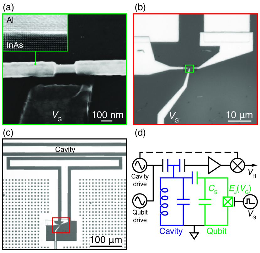
We have fabricated and measured two gatemon devices, which show similar performance. Except where noted, data is from the first device. The qubit features a single InAs SNS JJ shunted by a capacitance, Koch et al. (2007); Houck et al. (2007); Barends et al. (2013). The JJ is formed from a molecular beam epitaxy-grown InAs nanowire, 75 nm in diameter, with an in situ grown 30 nm thick Al shell. The Al shell forms an atomically precise SN interface leading to a proximity induced gap in the InAs core with a low density of states below the superconducting gap (hard gap) Krogstrup et al. ; Chang et al. (2015). By wet-etching away a 180 nm segment of the Al shell [Fig. 1(a)] a weak link in the superconducting shell is formed, creating the JJ. A supercurrent leaking through the semiconductor core links the unetched regions and determines the Josephson coupling energy, , which can be tuned by changing the electron density in the semiconductor core with a nearby side gate voltage, .
As with conventional transmons, the gatemon operates as an anharmonic LC oscillator with a nonlinear inductance provided by the JJ. The total capacitance of the gatemon qubit, , is determined by the capacitance of the T-shaped Al island to the surrounding Al ground plane, as shown in Fig. 1(c). The gatemon operates with , where the charging energy, . In this regime, decoherence due to either low frequency charge noise on the island or quasiparticle tunneling across the JJ is strongly suppressed. For many conducting channels in the wire, the qubit transition frequency is given by . The difference between and the next successive levels, , is the anharmonicity, . From microwave spectroscopy of our gatemon we estimate MHz.
The gatemon is coupled to a superconducting transmission line cavity with a bare resonance frequency GHz and quality factor, . The cavity is used for dispersive readout of the qubit with homodyne detection [Fig. 1(d)] Hom . Both the cavity and qubit leads are patterned by wet etching an Al film on an oxidised high resistivity Si substrate. The nanowire contacts and gate are also patterned from Al using a lift-off process with an ion mill step to remove the native Al2O3 prior to deposition.
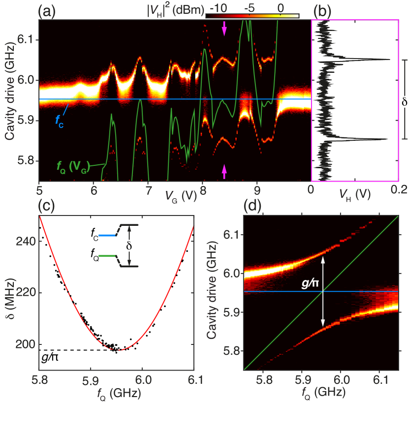
Gatemon-cavity coupling was investigated by measuring cavity transmission at low drive power as a function of the cavity drive frequency and gate voltage, , with [Fig. 2(a)]. Aperiodic fluctuations in the resonance as a function of , with regions of widely split transmission peaks, were observed [Fig. 2(b)]. These gate-dependent, repeatable fluctuations in the cavity resonance are associated with mesoscopic fluctuations in the nanowire transmission—appearing also as fluctuations of normal-state conductance, Doh et al. (2005)—which causes fluctuations in gatemon frequency, . The changing qubit frequency, in turn, pulls on the cavity resonance, resulting in the observed response. The split cavity peaks indicate hybridized qubit and cavity states in the strong coupling regime. The coupling strength, is found to exceed the qubit and cavity decoherence rates, allowing the vacuum Rabi splitting to be resolved Wallraff et al. (2004). Writing the hybridized qubit-cavity state frequencies as , Fig. 2(c) shows the splitting as a function of the qubit frequency . From the fit to the data we extract MHz. A parametric plot [Fig. 2(d)] of the data in Fig. 2(a), as a function of the extracted , reveals the avoided crossing for the hybridized qubit-cavity states Wallraff et al. (2004).
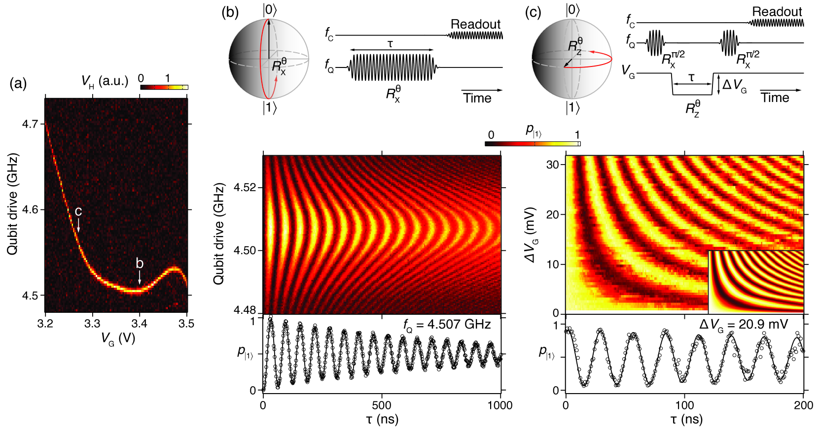
Demonstrations of qubit control were performed in the dispersive regime, . Figure 3(a) shows as a function of gate voltage, , obtained by measuring the qubit-state–dependent cavity response following a second 2 s microwave tone. When the qubit drive was on resonance with , a peak in the cavity response was observed, yielding a reproducible gate voltage dependence. At a fixed gate voltage [point b in Fig. 3(a)] we measure in Fig. 3(b) the cavity response while varying the qubit drive frequency and the length of the qubit microwave pulse to observe coherent Rabi oscillations. Data in the main panel of Fig. 3(b) were acquired over several hours, highlighting the stability of the device.
While pulsed microwaves allow rotations about axes in the - plane of the Bloch sphere, rotations about the -axis may be performed by adiabatically pulsing to detune the qubit resonance frequency. Such dynamic control of the qubit frequency is important for fast two qubit gate operations where the resonant frequencies of two coupled qubits are brought close to each other DiCarlo et al. (2009); Barends et al. (2014). Figure 3(c) shows rotations performed by first applying an pulse to rotate into the - plane of the Bloch sphere followed by a negative voltage pulse, , which causes the qubit state to precess about the -axis at the difference frequency, . Finally, a second pulse was applied to rotate the qubit out of the - plane and measure the resulting qubit state. The observed precession frequency is consistent with the predicted from the spectroscopy data in Fig. 3(a) [Fig. 3(c) main panel inset].
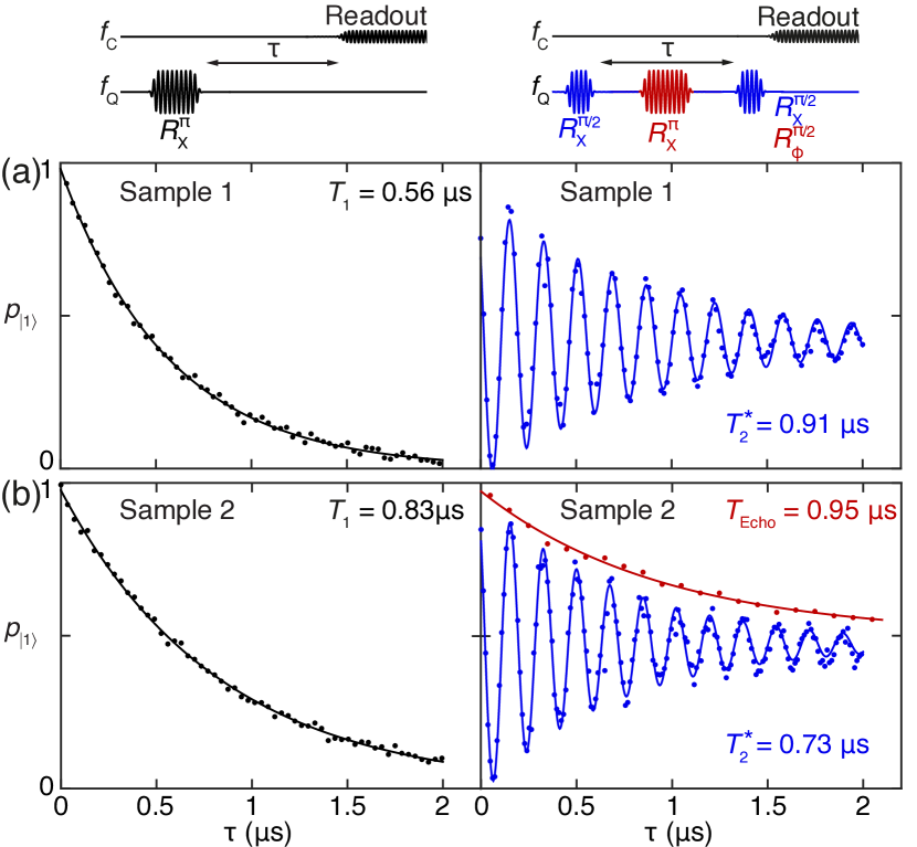
Gatemon coherence times were measured quantitatively in both devices [Fig. 4]. The relaxation time, , was measured by initializing the qubit to and varying the waiting time, , before readout, giving s for the first device, measured at operating point b in Fig. 3(a). The decay envelope of a Ramsey measurement [Fig. 4(a), right panel] gives a dephasing time, s at the same operating point. Noting that , we conclude that at this operating point, coherence was limited by energy relaxation. Figure 4(b) shows coherence times for the second sample, showing a slightly longer relaxation time, s [Fig. 4(b), left panel]. In this device, inhomogeneous dephasing time was shorter, s. In Fig. 4(b) right panel (in red) we show that applying a Hahn echo pulse sequence, which effectively cancels low frequency noise in , increases the dephasing time to s. This indicates a greater degree of low frequency noise in in the second device. The observation that does not reach indicates that higher frequency noise fluctuations faster than also contributes to dephasing.
Coherence times for these first-generation gatemon devices are comparable to SIS transmons reported a few years ago, where typically s Houck et al. (2008). Longer coherence times, s, have been reported more recently for planar transmon devices Chang et al. (2013). We anticipate that relaxation times can be substantially improved by removing the SiO2 dielectric layer O’Connell et al. (2008) and more careful sample processing to reduce interface losses in the capacitor Quintana et al. (2014), and increased magnetic and infrared radiation shielding Córcoles et al. (2011); Barends et al. (2011). This should in turn extend dephasing times and allow for the low frequency noise spectrum to be characterized using dynamical decoupling Bylander et al. (2011). Electrical noise coupling to due to charge traps at the nanowire surface could potentially be reduced through surface passivation Ford et al. (2012).
Conventional SIS transmons typically enable tunable frequency control by using two JJs in a SQUID geometry to create an effective flux tunable Josephson coupling energy. The qubit frequency is then controlled using superconducting current loops. The large (mA scale) currents used to control conventional flux-tuned transmons makes scaling to many qubits difficult using control electronics that pass into the cryogenic environment through normal coax lines, filters, and attenuators. On-chip voltage pulses are relatively easily screened, compared to flux pulses, which will reduce cross-talk between qubit control lines. Gatemons, with voltage tunable , also offer new possibilities for large scale superconducting architectures. For instance, FET-based cryogenic multiplexers Ward et al. (2013); Al-Taie et al. (2013) have recently been developed for millikelvin temperatures and would be well suited to gate control of large multi-gatemon circuits.
Finally, we note that the epitaxial InAs-Al nanowires are expected to support Majorana bound states Mourik et al. (2012); Das et al. (2012) due to the strong spin-orbit coupling and large factor (10) of InAs. Recent theoretical work has proposed using transmons to manipulate and probe topologically-protected qubits built from Majorana bound states Hassler et al. (2011); Ginossar and Grosfeld (2014). InAs nanowire-based gatemons could therefore be readily coupled to topological qubits made using the same material technology.
Acknowledgements.
We acknowledge financial support from Microsoft Project Q, Lundbeck Foundation, and the Danish National Research Foundation. K.D.P. was supported by a Marie Curie Fellowship.References
- Devoret and Schoelkopf (2013) M. H. Devoret and R. J. Schoelkopf, Science 339, 1169 (2013).
- Barends et al. (2014) R. Barends, J. Kelly, A. Megrant, A. Veitia, D. Sank, E. Jeffrey, T. C. White, J. Mutus, A. G. Fowler, B. Campbell, Y. Chen, Z. Chen, B. Chiaro, A. Dunsworth, C. Neill, P. O’Malley, P. Roushan, A. Vainsencher, J. Wenner, A. N. Korotkov, A. N. Cleland, and J. M. Martinis, Nature 508, 500 (2014).
- Bylander et al. (2011) J. Bylander, S. Gustavsson, F. Yan, F. Yoshihara, K. Harrabi, G. Fitch, D. G. Cory, Y. Nakamura, J.-S. Tsai, and W. D. Oliver, Nature Physics 7, 565 (2011).
- Kim et al. (2011) Z. Kim, B. Suri, V. Zaretskey, S. Novikov, K. D. Osborn, A. Mizel, F. C. Wellstood, and B. S. Palmer, Physical Review Letters 106, 120501 (2011).
- Manucharyan et al. (2012) V. E. Manucharyan, N. A. Masluk, A. Kamal, J. Koch, L. I. Glazman, and M. H. Devoret, Physical Review B 85, 024521 (2012).
- Paik et al. (2011) H. Paik, D. I. Schuster, L. S. Bishop, G. Kirchmair, G. Catelani, A. P. Sears, B. R. Johnson, M. J. Reagor, L. Frunzio, L. I. Glazman, S. M. Girvin, M. H. Devoret, and R. J. Schoelkopf, Physical Review Letters 107, 240501 (2011).
- Doh et al. (2005) Y. J. Doh, J. A. van Dam, A. L. Roest, E. P. A. M. Bakkers, L. P. Kouwenhoven, and S. De Franceschi, Science 309, 272 (2005).
- Abay et al. (2014) S. Abay, D. Persson, H. Nilsson, F. Wu, H. Q. Xu, M. Fogelström, V. Shumeiko, and P. Delsing, Physical Review B 89, 214508 (2014).
- (9) P. Krogstrup, N. L. B. Ziino, S. M. Albrecht, M. H. Madsen, E. Johnson, J. Nygård, C. M. Marcus, and T. S. Jespersen, Nature Materials, Advance Online Publication .
- Chang et al. (2015) W. Chang, S. M. Albrecht, T. S. Jespersen, F. Kuemmeth, P. Krogstrup, J. Nygård, and C. M. Marcus, Nature Nanotechnology 10, 232 (2015).
- Shim and Tahan (2014) Y.-P. Shim and C. Tahan, Nature Communications 5, (2014).
- Koch et al. (2007) J. Koch, T. Yu, J. Gambetta, A. Houck, D. Schuster, J. Majer, A. Blais, M. Devoret, S. Girvin, and R. Schoelkopf, Physical Review A 76, 042319 (2007).
- Houck et al. (2007) A. A. Houck, D. I. Schuster, J. M. Gambetta, J. A. Schreier, B. R. Johnson, J. M. Chow, L. Frunzio, J. Majer, M. H. Devoret, S. M. Girvin, and R. J. Schoelkopf, Nature 449, 328 (2007).
- (14) G. de Lange, B. van Heck, A. Brunol, D. van Woerkom, A. Geresdil, S. R. Plissard, E. P. A. M. Bakkers, A. R. Akhmerov, and L. DiCarlo, submitted .
- Barends et al. (2013) R. Barends, J. Kelly, A. Megrant, D. Sank, E. Jeffrey, Y. Chen, Y. Yin, B. Chiaro, J. Mutus, C. Neill, P. O’Malley, P. Roushan, J. Wenner, T. C. White, A. N. Cleland, and J. M. Martinis, Physical Review Letters 111, 080502 (2013).
- (16) The data in Fig. 2 were acquired using a vector network analyzer. For the Sample 1 data in Figs. 3 and 4 we mix down to dc and sample the homodyne response, . For the Sample 2 data in Fig. 4 we mix down to an intermediate frequency before sampling and then perform digital homodyne to extract the cavity phase response.
- Wallraff et al. (2004) A. Wallraff, D. I. Schuster, A. Blais, L. Frunzio, R.-S. Huang, J. Majer, S. Kumar, S. M. Girvin, and R. J. Schoelkopf, Nature 431, 162 (2004).
- DiCarlo et al. (2009) L. DiCarlo, J. M. Chow, J. M. Gambetta, L. S. Bishop, B. R. Johnson, D. I. Schuster, J. Majer, A. Blais, L. Frunzio, S. M. Girvin, and R. J. Schoelkopf, Nature 460, 240 (2009).
- Houck et al. (2008) A. A. Houck, J. A. Schreier, B. R. Johnson, J. M. Chow, J. Koch, J. M. Gambetta, D. I. Schuster, L. Frunzio, M. H. Devoret, S. M. Girvin, and R. J. Schoelkopf, Physical Review Letters 101, 080502 (2008).
- Chang et al. (2013) J. B. Chang, M. R. Vissers, A. D. Córcoles, M. Sandberg, J. Gao, D. W. Abraham, J. M. Chow, J. M. Gambetta, M. B. Rothwell, G. A. Keefe, M. Steffen, and D. P. Pappas, Applied Physics Letters 103, 012602 (2013).
- O’Connell et al. (2008) A. D. O’Connell, M. Ansmann, R. C. Bialczak, M. Hofheinz, N. Katz, E. Lucero, C. McKenney, M. Neeley, H. Wang, E. M. Weig, A. N. Cleland, and J. M. Martinis, Applied Physics Letters 92, 112903 (2008).
- Quintana et al. (2014) C. M. Quintana, A. Megrant, Z. Chen, A. Dunsworth, B. Chiaro, R. Barends, B. Campbell, Y. Chen, I. C. Hoi, E. Jeffrey, J. Kelly, J. Y. Mutus, P. J. J. O’Malley, C. Neill, P. Roushan, D. Sank, A. Vainsencher, J. Wenner, T. C. White, A. N. Cleland, and J. M. Martinis, Applied Physics Letters 105, 062601 (2014).
- Córcoles et al. (2011) A. D. Córcoles, J. M. Chow, J. M. Gambetta, C. Rigetti, J. R. Rozen, G. A. Keefe, M. B. Rothwell, M. B. Ketchen, and M. Steffen, Applied Physics Letters 99, 181906 (2011).
- Barends et al. (2011) R. Barends, J. Wenner, M. Lenander, Y. Chen, R. C. Bialczak, J. Kelly, E. Lucero, P. O’Malley, M. Mariantoni, D. Sank, H. Wang, T. C. White, Y. Yin, J. Zhao, A. N. Cleland, J. M. Martinis, and J. J. A. Baselmans, Applied Physics Letters 99, 113507 (2011).
- Ford et al. (2012) A. C. Ford, S. B. Kumar, R. Kapadia, J. Guo, and A. Javey, Nano Letters 12, 1340 (2012).
- Ward et al. (2013) D. R. Ward, D. E. Savage, M. G. Lagally, S. N. Coppersmith, and M. A. Eriksson, Applied Physics Letters 102, 213107 (2013).
- Al-Taie et al. (2013) H. Al-Taie, L. W. Smith, B. Xu, P. See, J. P. Griffiths, H. E. Beere, G. A. C. Jones, D. A. Ritchie, M. J. Kelly, and C. G. Smith, Applied Physics Letters 102, 243102 (2013).
- Mourik et al. (2012) V. Mourik, K. Zuo, S. M. Frolov, S. R. Plissard, E. P. A. M. Bakkers, and L. P. Kouwenhoven, Science 336, 1003 (2012).
- Das et al. (2012) A. Das, Y. Ronen, Y. Most, Y. Oreg, M. Heiblum, and H. Shtrikman, Nature Physics 8, 887 (2012).
- Hassler et al. (2011) F. Hassler, A. R. Akhmerov, and C. W. J. Beenakker, New Journal of Physics 13, 095004 (2011).
- Ginossar and Grosfeld (2014) E. Ginossar and E. Grosfeld, Nature Communications 5, 4772 (2014).