Growth-induced electron mobility enhancement at the \ceLaAlO3/\ceSrTiO3 interface
Abstract
We have studied the electronic properties of the 2D electron liquid present at the \ceLaAlO3/\ceSrTiO3 interface in series of samples prepared at different growth temperatures. We observe that interfaces fabricated at exhibit the highest low temperature mobility () and the lowest sheet carrier density (). These samples show metallic behavior and Shubnikov-de Haas oscillations in their magnetoresistance. Samples grown at higher temperatures () display carrier densities in the range of and mobilities of at . Reducing their carrier density by field effect to lowers their mobilites to bringing the conductance to the weak-localization regime.
Transition metal oxide heterostructures are very promising for nano-electronics since they allow the realization and tuning of new electronic phases Takagi and Hwang (2010); Mannhart and Schlom (2010); Zubko et al. (2011). In this respect, the interface formed by the two insulating perovskites \ceLaAlO3 (LAO) and \ceSrTiO3 (STO) is attracting a lot of attention due to the presence of a two-dimensional electron liquid (2DEL) Ohtomo and Hwang (2004), whose density can be tuned by electric field effect revealing a rich phase diagram Thiel et al. (2006); Caviglia et al. (2008). The origin of conduction is thought to be linked to the polar discontinuity between the two materials Nakagawa et al. (2006); Bristowe et al. (2011); Cancellieri et al. (2011); Stengel (2011).
A key ingredient for electronic applications is the charge mobility . LAO/STO interfaces typically display mobilities of at low temperature Reyren et al. (2007); Huijben et al. (2009), a value relatively low if electrons are provided by charge transfer. Hence, different studies have attempted to pinpoint the origin of the scattering mechanisms that limit the electron mobility at the interface. Thiel et al. observed a dramatic reduction of the conductance of the 2DEL when the density of dislocations is increased, and suggested that the region of influence of these line defects extends well beyond their physical size Thiel et al. (2009). In a related work Fix and coworkers considered the effect of vicinal substrates (i.e. step edge density) on mobility Fix et al. (2011). In agreement with previous results Bell et al. (2009a), the proximity of the charge distribution to the interface was pointed out to be an important factor in determining the scattering rate. Similar considerations were also raised for heterostructures of \ceLaTiO3/\ceSrTiO3 where the electric field effect was used to modify the charge profile Kim et al. (2010). The role of the LAO thickness on the electron mobility at the LAO/STO interface was also studied, revealing a strongly reduced mobility in heterostructures made of thick LAO films Bell et al. (2009b). More recently, the presence of tetragonal domains in STO (at low temperature) was demonstrated to alter locally the conductance Kalisky et al. (2013); Honig et al. (2013). Finally, the control of the LAO surface state was shown to be an efficient lever to enhance the interfacial electron mobility Xie et al. (2013); Huijben et al. (2013); Bristowe et al. (2011).
In this letter, we perform a systematic study of the effect of the growth temperature () on the transport properties of the LAO/STO interface. In samples grown at , called “standard” samples, carrier densities in the range are observed while mobility at low temperature reaches . Reducing the growth temperature to leads to a lower carrier density, of the order of a few , and a much higher mobility reaching , allowing the observation of 2D-quantum oscillations Caviglia et al. (2010a). Concomitantly, whereas the Hall resistance is found to be temperature dependent and to display a non-linear behavior at low temperature for “standard” samples, is independent and linear for interfaces grown at . We also show that, using the electric field effect to reduce the Hall carrier density of high samples (having initial high carrier densities) to values observed in low samples, the magnetoresistance differs from the one observed for high-mobility samples.
LAO thin films were grown by pulsed laser deposition at an oxygen pressure of and post-annealed for one hour at in of oxygen Cancellieri et al. (2010). The KrF excimer laser was set for a fluence of with a repetition rate of . Growth temperatures ranged from to , as measured on the substrate by an optical pyrometer. The thickness of the LAO layer was kept within the range of 5 to 10 unit cells Cancellieri et al. (2011). Periodic oscillations in the reflection high energy electron diffraction (RHEED) intensity reveal a layer-by-layer growth for all . The RHEED diffraction pattern indicates that the 2-dimensional character is maintained even for the lowest . Atomic force microscopy confirms that the film surfaces reproduce the step-and-terrace morphology of the TiO2-terminated (001) STO substrates 111We use STO substrates from CrysTec GmbH that are already HF treated and high-temperature annealed to provide \ceTiO2 termination. Before growth, the sample holder with the substrate is annealed in vacuum for 30 min at a temperature of .. X-ray scans for the 001 reflections show diffraction peaks with finite size fringes in agreement with the layer thickness and an intensity independent of . The above structural characterization revealed no effect of the substrate temperature on the growth mode or the crystalline quality of thin LAO layers.
For DC transport measurements, wide Hall bridges were patterned using standard photolithography techniques and an amorphous STO hard mask Stornaiuolo et al. (2012).
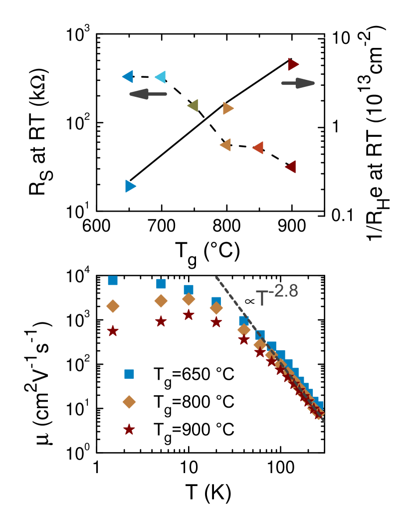
In the top panel of Fig. 1, the room temperature (RT) sheet resistance () is plotted as a function of the growth temperature. We note that upon decreasing down to the RT sheet resistance increases by roughly an order of magnitude. This evolution is mainly related to a reduction of the carrier density, the increase in the Hall mobility being less than a factor of two 222The estimation of the carrier density is obtained from the Hall constant at where the Hall resistance is linear.. The lower panel of Fig. 1 shows a large increase in the electron mobility at low temperatures : as is reduced from 900 to , goes from 600 to at .
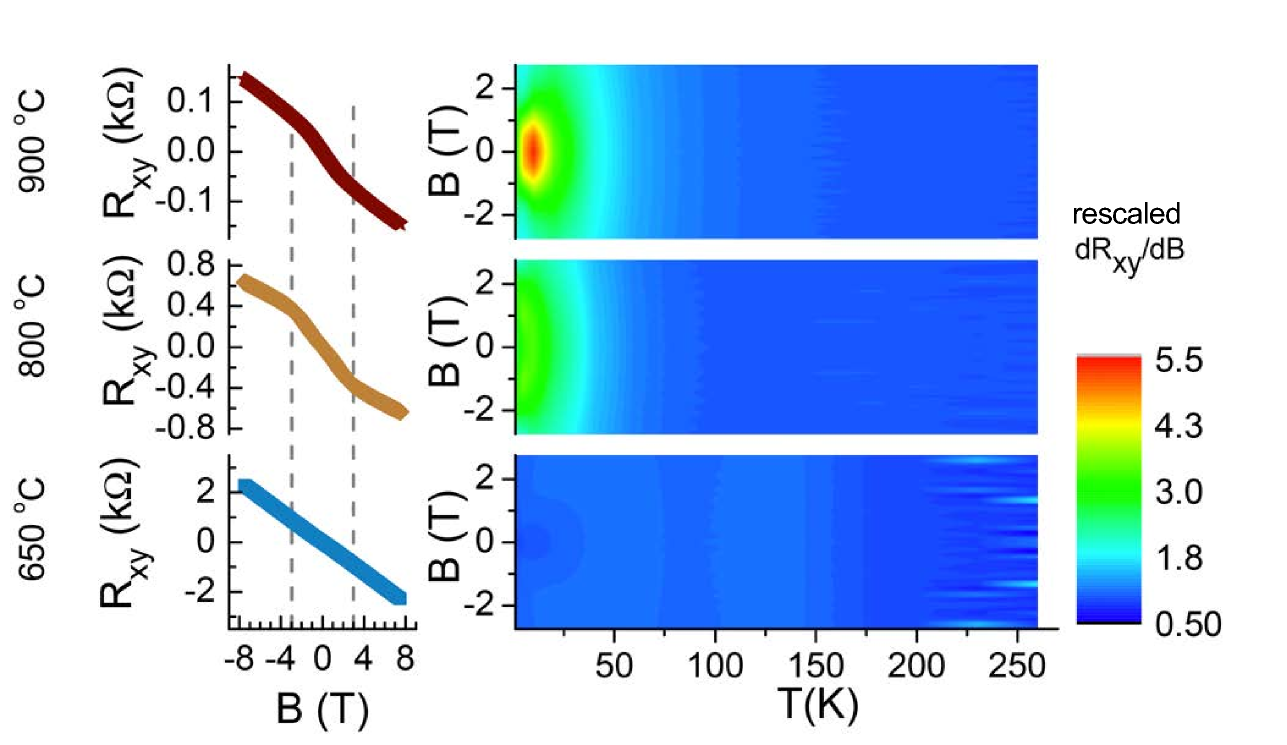
In Fig. 2, we plot (left) the Hall resistance measured at as a function of the magnetic field and (right) its field derivative as a function of the magnetic field and temperature for heterostructures grown at three different temperatures.
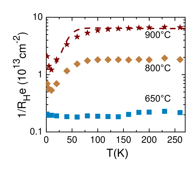
Samples grown at = exhibit a linear essentially temperature independent. For growth temperatures of 800 and , the Hall resistance displays a more complex behavior. In the 100- temperature range, is linear in magnetic field and its derivative () is temperature independent 333We note, though, that depending on the photo-doping level Tebano2012; Guduru2013, some temperature dependence of the Hall effect above can sometimes be observed.. Below , the Hall response becomes a non-linear function of the magnetic field and its low field derivative increases at low temperature. The temperature dependence of the inverse Hall constant estimated at is shown in Fig. 3.
Analyzing the low temperature magnetotransport for samples grown at with a two channel conduction model reveals contributions from a band with a low carrier density () and a high mobility (in the range of ) and from a band with a higher carrier density () and low mobility (in the range of ), in agreement with previous reports Ben Shalom et al. (2010); Lerer et al. (2011). The dependence on magnetic field of the low field for the different temperatures can be captured by the same two-band model (see Fig. 3) taking into account the temperature dependence of the scattering time (, and being the elastic and the inelastic scattering times respectively and , see Fig. 1) and keeping the density of each band constant 444The elastic scattering time for each band is calculated from the respective mobility obtained from the two band fit in magnetic field while the inelastic scattering time is considered to be independent off the carrier type.. Thus the temperature and field dependencies of the Hall resistance can be quantitatively explained by the presence of carriers with different mobilities in the system. This analysis also suggests that the correct estimate of the total mobile carrier density can be obtained from the slope of the Hall effect at high fields in the low range or above Takahashi et al. (2006).
The presence of charge carriers with different masses (and thus different mobilities) at the LAO/STO interface has been anticipated by ab initio calculations Pentcheva and Pickett (2006); Popović et al. (2008); Son et al. (2009); Delugas et al. (2011); Stengel (2011). The predicted electronic structure of the confined electron liquid is characterized by a lifting of the degeneracy of the 3 orbitals with the lowest sub-band(s) having a lower energy than the lowest sub-bands. Experimental evidence supporting this model came from linear dichroism measurements Salluzzo et al. (2009) providing an estimate of their splitting of . According to this picture, for large densities, the Fermi level should cross sub-bands with and (, being the electron mass) character and then multi-channel conduction is expected. For low carrier densities only (a) sub-band(s) with an effective mass should contribute to the transport. However, more recently resonant photoemission spectroscopyCancellieri et al. (2014) supported by ab initio calculations have revealed that the electronic band structure is modified along with the carrier density, probably related to a change in the confinement potential; sub-bands are still observed at low carrier density interfaces.
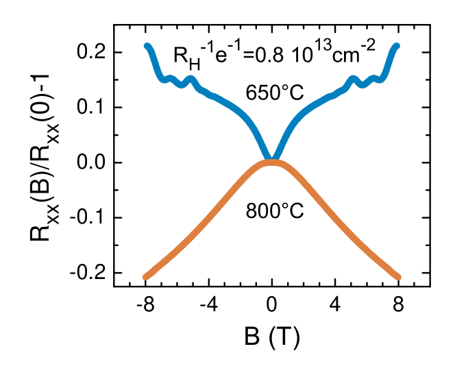
Fig. 4 shows the change in magnetoresistance at for a sample grown at (): it amounts to 20% for a magnetic field of . Above , we observe the appearance of Shubnikov-de Haas oscillations. This large magnetoresistance suggests that also for these low carrier densities multiple channels contribute to the transport. Further evidence of the population of orbitals in LAO/STO interfaces grown at were provided recently by detailed analyses of the Shubnikov-de Haas oscillations Fête et al. (2014).
In order to shed further light on the effect of the carrier density on the sample mobility, we performed a series of field effect experiments in samples grown at . In agreement with Bell and coworkers Bell et al. (2009a), we find that the dominant effect of the electric field in the back gate geometry is the modulation of the mobility. In Fig. 4 we show also the low temperature magnetoresistance of a sample grown at . Using field effect, its carrier density was tuned to match that of the high mobility sample 555In this carrier density range, the Hall effect is linear in magnetic field for both type of interfaces. (). As a result, the mobility was reduced to . Fig. 4 shows that whereas the high mobility sample displays a positive magnetoresistance, the change in resistance of the sample is negative and on the scale of . This behavior has been shown to be the signature of weak-localization Caviglia et al. (2010b). This comparison reveals strikingly different magnetotransport behavior in samples with similar carrier densities and confirm the low dimensional nature of this conducting system where transport regimes are determined by the characteristic scattering lengths (elastic, phase, spin-orbit) more than their carrier density.
These results emphasize the open question on the origin of the carrier mobility at the LAO/STO interface : what is determining the high observed in low samples compared with the low measured in high samples for the same doping ? The shape of the confinement potential is responsible for the proximity of the conducting layer to the interface. Hence, any disorder, as for instance interface intermixing, would affect differently the electron mobility depending on the charge profile Bell et al. (2009a). In this scenario, the electric field effect results suggest that the charge profile at the same density can be different. On the other hand, if interface perfection is modified by the growth temperature Ohnishi et al. (2004), then the same charge profile would generate a different electronic mobility.
Both situations can be at play in our samples; further detailed structural analyses, like surface x-ray diffraction, could help to address this important point.
In conclusion, transport properties of \ceLaAlO3/\ceSrTiO3 interfaces were shown to be very sensitive to the sample growth temperature. For a substrate temperature of , the carrier mobility reaches and Shubnikov-de Haas oscillations appear in the magnetotransport. These samples also show a low carrier density of . Field effect experiments reveal that the carrier density is not the parameter determining the mobility. Further optimization of the growth conditions remains key to the observation of clean superconductivity and other quantum effects in this complex oxide 2D electron system.
The authors are grateful to M. Lopes and S. C. Müller for their technical assistance. This work was supported by the Swiss National Science Foundation through the NCCR MaNEP and Division II, by the Institut Universitaire de France (MG) and has received funding from the European Research Council under the European Union’s Seventh Framework Programme (FP7/2007-2013) / ERC Grant Agreement n∘ 319286 (Q-MAC).
References
- Takagi and Hwang (2010) H. Takagi and H. Y. Hwang, Science 327, 1601 (2010).
- Mannhart and Schlom (2010) J. Mannhart and D. G. Schlom, Science 327, 1607 (2010).
- Zubko et al. (2011) P. Zubko, S. Gariglio, M. Gabay, P. Ghosez, and J.-M. Triscone, Annu. Rev. Condens. Matter Phys. 2, 141 (2011).
- Ohtomo and Hwang (2004) A. Ohtomo and H. Y. Hwang, Nature 427, 423 (2004).
- Thiel et al. (2006) S. Thiel, G. Hammerl, A. Schmehl, C. W. Schneider, and J. Mannhart, Science 313, 1942 (2006).
- Caviglia et al. (2008) A. D. Caviglia, S. Gariglio, N. Reyren, D. Jaccard, T. Schneider, M. Gabay, S. Thiel, G. Hammerl, J. Mannhart, and J.-M. Triscone, Nature 456, 624 (2008).
- Nakagawa et al. (2006) N. Nakagawa, H. Y. Hwang, and D. A. Muller, Nat. Mater. 5, 204 (2006).
- Bristowe et al. (2011) N. C. Bristowe, P. B. Littlewood, and E. Artacho, Phys. Rev. B 83, 205405 (2011).
- Cancellieri et al. (2011) C. Cancellieri, D. Fontaine, S. Gariglio, N. Reyren, A. D. Caviglia, A. Fete, S. J. Leake, S. A. Pauli, P. R. Willmott, M. Stengel, P. Ghosez, and J.-M. Triscone, Phys. Rev. Lett. 107, 56102 (2011).
- Stengel (2011) M. Stengel, Phys. Rev. Lett. 106, 136803 (2011).
- Reyren et al. (2007) N. Reyren, S. Thiel, A. D. Caviglia, L. F. Kourkoutis, G. Hammerl, C. Richter, C. W. Schneider, T. Kopp, A.-S. Rüetschi, D. Jaccard, M. Gabay, D. A. Muller, J.-M. Triscone, and J. Mannhart, Science 317, 1196 (2007).
- Huijben et al. (2009) M. Huijben, A. Brinkman, G. Koster, G. Rijnders, H. Hilgenkamp, and D. H. A. Blank, Adv. Mater. 21, 1665 (2009).
- Thiel et al. (2009) S. Thiel, C. Schneider, L. Kourkoutis, D. Muller, N. Reyren, A. Caviglia, S. Gariglio, J.-M. Triscone, and J. Mannhart, Phys. Rev. Lett. 102, 046809 (2009).
- Fix et al. (2011) T. Fix, F. Schoofs, Z. Bi, A. Chen, H. Wang, J. L. MacManus-Driscoll, and M. G. Blamire, Appl. Phys. Lett. 99, 022103 (2011).
- Bell et al. (2009a) C. Bell, S. Harashima, Y. Kozuka, M. Kim, B. G. Kim, Y. Hikita, and H. Y. Hwang, Phys. Rev. Lett. 103, 226802 (2009a).
- Kim et al. (2010) J. S. Kim, S. S. A. Seo, M. F. Chisholm, R. K. Kremer, H.-U. Habermeier, B. Keimer, and H. N. Lee, Phys. Rev. B 82, 201407 (2010).
- Bell et al. (2009b) C. Bell, S. Harashima, Y. Hikita, and H. Y. Hwang, Appl. Phys. Lett. 94, 222111 (2009b).
- Kalisky et al. (2013) B. Kalisky, E. M. Spanton, H. Noad, J. R. Kirtley, K. C. Nowack, C. Bell, H. K. Sato, M. Hosoda, Y. Xie, Y. Hikita, C. Woltmann, G. Pfanzelt, R. Jany, C. Richter, H. Y. Hwang, J. Mannhart, and K. A. Moler, Nat. Mater. 12, 1091 (2013).
- Honig et al. (2013) M. Honig, J. a. Sulpizio, J. Drori, A. Joshua, E. Zeldov, and S. Ilani, Nat. Mater. 12, 1112 (2013).
- Xie et al. (2013) Y. Xie, C. Bell, Y. Hikita, S. Harashima, and H. Y. Hwang, Adv. Mater. 25, 4735 (2013).
- Huijben et al. (2013) M. Huijben, G. Koster, M. K. Kruize, S. Wenderich, J. Verbeeck, S. Bals, E. Slooten, B. Shi, H. J. a. Molegraaf, J. E. Kleibeuker, S. van Aert, J. B. Goedkoop, A. Brinkman, D. H. a. Blank, M. S. Golden, G. van Tendeloo, H. Hilgenkamp, and G. Rijnders, Adv. Funct. Mater. 23, 5240 (2013).
- Caviglia et al. (2010a) A. D. Caviglia, S. Gariglio, C. Cancellieri, B. Sacépé, A. Fete, N. Reyren, M. Gabay, A. F. Morpurgo, and J.-M. Triscone, Phys. Rev. Lett. 105, 236802 (2010a).
- Cancellieri et al. (2010) C. Cancellieri, N. Reyren, S. Gariglio, A. D. Caviglia, A. Fete, and J.-M. Triscone, EPL (Europhysics Lett. 91, 17004 (2010).
- Note (1) We use STO substrates from CrysTec GmbH that are already HF treated and high-temperature annealed to provide \mhchem@ce@xiiiTiO2 termination. Before growth, the sample holder with the substrate is annealed in vacuum for 30 min at a temperature of .
- Stornaiuolo et al. (2012) D. Stornaiuolo, S. Gariglio, N. J. G. Couto, A. Fête, a. D. Caviglia, G. Seyfarth, D. Jaccard, a. F. Morpurgo, and J.-M. Triscone, Appl. Phys. Lett. 101, 222601 (2012).
- Note (2) The estimation of the carrier density is obtained from the Hall constant at where the Hall resistance is linear.
- Note (3) We note, though, that depending on the photo-doping level Tebano2012; Guduru2013, some temperature dependence of the Hall effect above can sometimes be observed.
- Ben Shalom et al. (2010) M. Ben Shalom, A. Ron, A. Palevski, and Y. Dagan, Phys. Rev. Lett. 105, 206401 (2010).
- Lerer et al. (2011) S. Lerer, M. Ben Shalom, G. Deutscher, and Y. Dagan, Phys. Rev. B 84, 075423 (2011).
- Note (4) The elastic scattering time for each band is calculated from the respective mobility obtained from the two band fit in magnetic field while the inelastic scattering time is considered to be independent off the carrier type.
- Takahashi et al. (2006) K. S. Takahashi, M. Gabay, D. Jaccard, K. Shibuya, T. Ohnishi, M. Lippmaa, and J.-M. Triscone, Nature 441, 195 (2006).
- Pentcheva and Pickett (2006) R. Pentcheva and W. Pickett, Phys. Rev. B 74, 035112 (2006).
- Popović et al. (2008) Z. Popović, S. Satpathy, and R. Martin, Phys. Rev. Lett. 101, 256801 (2008).
- Son et al. (2009) W.-j. Son, E. Cho, B. Lee, J. Lee, and S. Han, Phys. Rev. B 79, 245411 (2009).
- Delugas et al. (2011) P. Delugas, A. Filippetti, V. Fiorentini, D. I. Bilc, D. Fontaine, and P. Ghosez, Phys. Rev. Lett. 106, 166807 (2011).
- Salluzzo et al. (2009) M. Salluzzo, J. Cezar, N. Brookes, V. Bisogni, G. De Luca, C. Richter, S. Thiel, J. Mannhart, M. Huijben, A. Brinkman, G. Rijnders, and G. Ghiringhelli, Phys. Rev. Lett. 102, 166804 (2009).
- Cancellieri et al. (2014) C. Cancellieri, M. L. Reinle-Schmitt, M. Kobayashi, V. N. Strocov, P. R. Willmott, D. Fontaine, P. Ghosez, a. Filippetti, P. Delugas, and V. Fiorentini, Phys. Rev. B 89, 121412 (2014).
- Fête et al. (2014) A. Fête, S. Gariglio, C. Berthod, D. Li, D. Stornaiuolo, M. Gabay, and J.-M. Triscone, New J. Phys. 16, 112002 (2014).
- Note (5) In this carrier density range, the Hall effect is linear in magnetic field for both type of interfaces.
- Caviglia et al. (2010b) A. D. Caviglia, M. Gabay, S. Gariglio, N. Reyren, C. Cancellieri, and J.-M. Triscone, Phys. Rev. Lett. 104, 126803 (2010b).
- Ohnishi et al. (2004) T. Ohnishi, K. Shibuya, M. Lippmaa, D. Kobayashi, H. Kumigashira, M. Oshima, and H. Koinuma, Appl. Phys. Lett. 85, 272 (2004).