Charge transport through a semiconductor quantum dot-ring nanostructure
Abstract
Transport properties of a gated nanostructure depend crucially on the coupling of its states to the states of electrodes. In the case of a single quantum dot the coupling, for a given quantum state, is constant or can be slightly modified by additional gating. In this paper we consider a concentric dot–ring nanostructure (DRN) and show that its transport properties can be drastically modified due to the unique geometry. We calculate the dc current through a DRN in the Coulomb blockade regime and show that it can efficiently work as a single electron transistor or a current rectifier. In both cases the transport characteristics strongly depends on the details of the confinement potential. The calculations are carried out for low and high bias regime, the latter being especially interesting in the context of current rectification due to fast relaxation processes.
pacs:
73.23.Hk, 73.21.La, 73.22.-f1 Introduction
In order to meet growing demand for small scale, low-power consuming devices one has to downscale transistors and logic circuits and to work with a small number of carriers. The natural limit for lowering carrier density is single charge electronics, where phenomena such as electric current can be controlled with single electron precision [1, 2]. Contrary to modern mass production electronics, single and a few electron devices exhibit purely quantum mechanical effects such as resonant tunneling [1, 3, 4, 2, 5] or quantum entanglement [6, 7, 8]. Apart from direct applications in nanoelectronics they are also perfect tools for probing fundamental problems in single and many-body physics. During the last decade a lot of research has been devoted to study the electronic properties of qauntum dots (QD) [5, 9, 10, 11, 12, 13, 14]. For sufficiently low temperatures the discretness of the energy spectrum of these systems can be clearly visible in transport experiments as Coulomb peaks [15, 1, 4, 16] that demonstrate succesive charging and discharging of the QD by single electrons. The Coulomb blockade phenomenon, where the charging energy forbids an electron to jump to the QD, is the basis for most of the applications of QDs [17, 18, 19]. Quantum dots arranged into double, triple or more complex systems [20, 21, 22, 23, 24, 25, 26, 27, 28] exhibit abundance of quantum states which manifest themselves, e.g., in Pauli spin blockade [29, 30] current or heat rectification [13] effects.
Another class of interesting quantum systems are quantum rings (QR) [31, 32, 33, 34, 35]. Due to different from QDs geometry the phenomena observed in QRs are very sensitive to phase coherence of the electronic wave function. These are, e.g., the Aharonov-Bohm effect demonstrating modification of the electron wave function by a vector potential [36] or persistent currents, i.e., ground state currents that flow in QR even without an external magnetic field [37, 38, 39].
In this paper we focus on a complex nanostructure that combines the two mentioned above, topologically different components: a quantum dot and a quantum ring. The constituents are aligned concentrically (QD is surrounded by QR) so that the system conserves the circular symmetry. The dot-ring nanostructure (DRN) has already been fabricated by pulsed droplet epitaxy [40, 41] with full control of the growth process. It can also be made by using atomic force microscope to locally oxidize the surface of a sample [12] or by lithography. Another method would be to grow a core-shell nanowire [42, 43] of, e.g., (In,Ga)As, where the core and shell parts are separated by a tunneling barrier. Then by cutting a slice of it one can form a DRN. A DRN exhibits a large variety of quantum states [44] what leads to many interesting features.
It has been recently shown [45, 46] that many measurable properties of a DRN, like spin relaxation or optical absorption, can be widely changed by a modification of the confinement potential of the DRN demonstrating its very high controllability and flexibility. These characteristics are mostly determined by the relative distribution of the wave functions in a DRN that, in turn, can be changed by external gates or fields. The purpose of this study is to demonstrate that also conducting properties of a DRN are very sensitive to the details of confinement and that we can realize different single electron devices on this complex structure. Unlike field effect transistors, single electron devices are based on intrinsically quantum phenomenon, namely the tunnel effect. In this case transport properties are mostly determined by the tunneling rates ’s, which depend on the overlap of the DRN states with the states of the electrodes. These parameters, in turn, depend crucially on the localization of the electron wave function: states localized in QD (QR) are weakly (strongly) coupled to the electrodes. Thus ’s may strongly depend on the quantum state and have to be determined for each state individually. This property demonstrates one of the advantages of the DRN over QDs, where the possible changes of the couplings are orders of magnitude smaller.
We discuss charge transport through a DRN in the Coulomb blockade regime near the transition, i.e., when only one electron at a time can tunnel through a DRN between the source (S) and drain (D) electrodes. Throughout this paper we assume the magnetic field and therefore neglect the electron spin. We show that one can tune the device parameters so that it can work as: (i) single electron transistor [4, 47] and (ii) electrical current rectifier. The paper is organized as follows: In Sec. 2 we present a general theoretical background that will be needed to study the transport properties of DRNs. In Sec. 3 we demonstrate how by changing the parameters of the confinement potential we can control single electron tunneling and build a single electron transistor (SET). In Sec. 4 we demonstrate that a DRN can be used as a current rectifier. The results are summarized in Sec. 5.
2 Basic formulas and mechanisms
We consider a quasi–two–dimensional circularly symmetric dot-ring nanostructure. The DRN, placed in the plane, is defined by a specific confinement potential, that we will discuss below. We assume that the confinement in the (growth) direction is much stronger than the lateral confinement and consequently, the -plane motion and the vertical one can be decoupled. Then, we can write the electron wave function as a product
| (1) |
where the vector lies in the -plane. Additionally, we assume that the electron is always in the lowest energy state of a quantum well in direction and that the potential of the well in direction is infinite. With these assumptions is given by
| (2) |
where is the height of the structure.
In order to discuss the in–plane confinement potential that forms the DRN we introduce the following notation . Then the DRN is defined by a potential and occupied by a single electron. The DRN is composed of a QD surrounded by a QR and separated from the ring by a potential barrier . A cross section and a top view of a DRN with explanation of symbols used throughout the text is presented in figure 1.
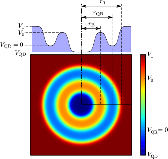
In particular, we assume in our model calculations the radius of the DRN nm. The depth of the quantum well forming the DRN is meV and the zero potential energy is set at the level of , i.e., the potential well offset is equal . The calculations are performed for InGaAs systems (with the effective electron mass ). The results are presented for meV and for the sample thickness nm, if not stated otherwise.
We solve numerically the Schrödinger equation assuming the Gaussian form of [45]. The energy spectrum consists of a set of discrete states due to radial motion with radial quantum numbers , and rotational motion with angular momentum quantum numbers . The energy spectrum as a function of is shown in figure 2.
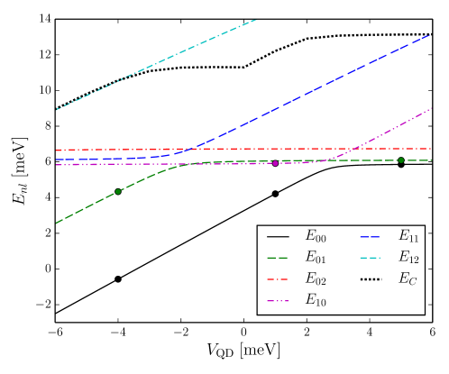
The states situated in QD exhibit an increase of the energy with increasing , whereas those situated in QR have the energy (nearly) constant. The single particle wave function in the -plane, i.e., the DRN plane, is of the form
| (3) |
with the radial part .
.
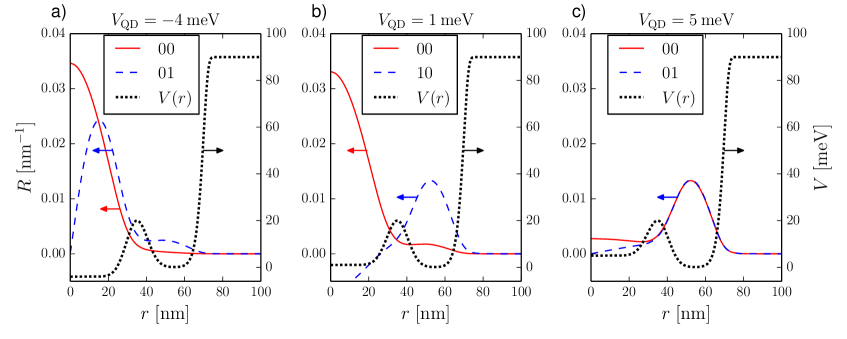
As already mentioned, the main advantage of the DRN is the controllability of the shape and the distribution of the electron wave functions. For instance, if the minimum of the potential of the QD part is much deeper than the potential of the QR, the electrons are located mainly in the QD and the effective size of the ground state (G) wave function is small. On the other hand, if the ring’s potential is much deeper electrons occupy mostly states in the QR part and the G wave function is much broader. What is more, by fine–tuning the confinement potential we can control positions of individual states. This way we are able to have, e.g., the ground state located in the QD, whereas the first excited state (E) in the QR and so on. The distributions of the wave functions of the two lowest energy states for three different values of are presented in figure 3. One can see there the case where both the G and E wave functions are in the QD for meV (figure 3a), the E wave function is in the QR, whereas the G wave function is still in the QD for meV (figure 3b), and finally, for meV both the G and E wave functions are in the QR (figure 3c).
The DRN is coupled via tunnel barriers to the S and D electrodes. We assume that one or a few () single–electron states are in the bias window
| (4) |
where and are the respective chemical potentials, represents a set of quantum numbers and we start the numbering of the energy levels from (the ground state). Charge transport through a DRN depends crucially on the coupling strength of its states to the electrodes what is dependent on the wave function overlap that enters the electron tunneling matrix element. Because we are able to control the shape and distribution of the DRN wave functions, we can control the overlap, which, in turn, allows us to control the transport properties.
The tunneling rates ’s are calculated microscopically for each state independently. We follow Bardeen’s approach [48], where
| (5) |
Within the framework of this method two separate sets of states are considered: one solves the Schrödinger equation for the DRN and one for the electrode. It is implicitly assumed that the wave functions of the two subsystems are orthogonal.
Enforcing this assumption the Bardeen tunneling matrix element in two dimensions is given by
| (6) |
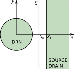
where are wave functions in the electrode and are wave functions in the DRN. The integral is calculated along the line (see figure 4). The explicit form of is given in the Appendix.
2.1 Phonon relaxation in a DRN
When more that one state is included in the transport process one has to take into account mechanisms that allow transitions between the states, i.e., relaxation to the lower energy states. One of the most important and unavoidable mechanisms of scattering in solid state systems is the interaction with lattice phonons. For low-dimensional semiconducting systems as QDs and QRs the dominant process is the electron-acoustic phonon interaction. This is because the energy distance between the electronic states is small comparing to the optical phonon energy [49, 33, 50].
In this section we calculate phonon emission relaxation rates due to interaction of an electron with piezoelectric (PZ) and deformational (DF) phonons. The electron-phonon scattering rate due to transition from the initial state to the final state with emission of an acoustic phonon can be calculated using Fermi’s golden rule (),
| (7) |
where is the phonon wave vector, () is the energy of the final (initial) electron state, is the energy of a phonon and is the polarization index. The interaction operator is given by
| (8) |
where is the total scattering matrix element [33]
| (9) |
Because in this paper we focus mainly on transport properties of the DRN, we follow the reference [33] and use angular averaged piezoelectric coupling matrix element for longitudinal and transverse phonon modes. Thus, the total electron-phonon scattering matrix element can be written as [33, 51]
| (10) |
where () is the deformational (piezoelectric) potential constant, is the crystal density, is the sound velocity, and is the volume. After Refs. [33, 51] we assume J and J2m-2. The total relaxation rate from state to state at can be written as
| (11) | |||||
where and is the radial part of the in-plane electron wave function . The integral over is given by , where
| (12) |
and the integral over can be expressed by the Bessel function. Finally, the relaxation rate can be written as
| (13) |
where
| (14) |
Apart from material constants the factors that affect this rate are the energy gap between states and , i.e., , the mutual distribution of the wave functions given by and , and the thickness of the structure . Function describes how phonons emitted in different directions contribute to the relaxation process. The relaxation through phonons emitted at a given angle depends on through function given in equation (12). On the one hand, since its argument is the relaxation is independent of the thickness for phonons with wave vectors parallel to the plane (). On the other hand, there is a strong dependence of the relaxation rate on for phonons emitted in the direction perpendicular to nanostructure. Figure 5 shows . One can see there that for a significant contribution to the relaxation comes only from phonons with wavelength larger then .
Figure 6 shows the square of the function given by equation (14) for . The value of and the radial parts of the wave functions and have been calculated for two different values of . In the case presented in the left panel () the bottom of the QD potential is much below the bottom of the QR potential. Therefore, the wave functions are situated mainly in the QD part of the DRN, where the energy level spacing is large (see figure 2). On the other hand, the right panel presents the case of where the bottom of the QD potential is above the bottom of the QR potential. In this situation the wave functions are situated mainly in the QR part of the DRN and, as it infers from figure 2, the level spacing is small. Figure 6 allows one to analyze the directions of phonons emission in two presented cases. Namely, in the left panel () function describing the phonon emission is peaked within the range of low values of . This indicates that phonons are emitted mostly perpendicularly to the DRN, which is the direction of the strongest confinement [49]. In the complementary case presented in the right panel (), it is not possible to point out a specific direction of emission (it varies with a particular transition , note the difference in the scales on the horizontal axes).
Figure 7 shows typical examples of how the relaxation rates are affected by changing the position of the bottom of the QD potential from below to above the bottom of the QR potential (). Figure 7a shows the relaxation rate from state to the ground state . For large, negative value of both the wave functions and are positioned in the QD what gives fast relaxation with rates of the order of GHz. With increasing the excited state moves over to the QR leading to the decrease of the overlap between the wave functions what, in turn, results in the decrease of . For further increased both the ground and the excited state are situated in the QR, the overlap increases and the relaxation rate increases again. Figure 7b presents the relaxation rate from state to the ground state. In this case for small the ground state is localized in the QD, while the excited state is mostly positioned in the QR. Therefore, the overlap of the corresponding wave functions is small, what in turn results in a slow relaxation. With the increase of the ground state starts to move over to the QR and the overlap with starts to rise. One observes it as a sharp increase of the relaxation rate . However, with further increase of the ground state remains in the QR, yet the excited state moves over to the QD and changes sign. This altogether causes the decrease of the relaxation rate. Figure 7c presents the relaxation rate between states and , a transition that is a part of an indirect relaxation process. What is clearly visible at first glance is the abrupt decrease of when the states cross (compare figure 2). In the range of from -2 meV to 2 meV the overlap between and is strong. Thus, the resulting values of the relaxation rate are high.
As it was already mentioned, the phonon emission at different angles is strongly dependent on the distribution of the wave functions (see figure 6). This, in turn affects the dependence of the relaxation rates on the sample thickness . In figure 8 we present the relaxation rate as a function of . Its dependence on is pronounced for low values of , when the wave functions are situated mainly in the QD region of the DRN. In accordance with what was reported in Ref. [33] for QD’s, we also observe oscillations of the relaxation rates as a function of the sample thickness in the range of negative values of (yet in figure 8 we present only a part of the noted oscillations). In the range of low values of the level spacings are of the order of single meV’s (figure 2). The corresponding wavelengths of emitted phonons are of the order of the sample thickness (couple of nm’s). This match results in the strong increase of the relaxation rates for such . In the complementary range of , where the bottom of the QD potential is above the bottom of the QR potential, the level spacings are of order of 0.1 meV. Then, the corresponding wavelengths of emitted phonons are significantly larger than the sample thickness and we do not observe any strong dependence of on the thickness of the structure . Additionally, we would like to stress the strong dependence of the relaxation rates for all other transitions on (not shown).
3 Single electron transistor
We are now ready to discuss the transport properties of the DRN. We evaluate the current given the energy spectrum and the subsequent relaxation and tunnel rates. We discuss below sequential tunneling current in the Coulomb blockade regime near the transition and neglect higher order tunneling events [52]. In the pure quantum dot case SET is switched to the conducting state when some energy level, shifted by gate voltage, enters the bias window. The current exhibits then the current peak [5]. In case of the DRN the mechanism is different. We keep one or a few states in the bias window and manipulate the distribution of the wave functions to get a proper transistor behavior. The principle of operations in is to control the energy states and tunnel couplings by means of gate voltages and . Many investigations of transport behavior make use of the high tunability of the tunnel barriers by applying voltage pulses [52]. In our approach we utilize instead the high tunability of the electron states in the DRN while keeping the barrier parameters constant. We assume that the bias window is smaller than the charging energy , so that only a single electron at a time can be transmitted through the DRN, . In order to determine for what values of the model parameters this condition can be fulfilled we calculate for the DRN. The interaction energy of two particles confined in the potential was calculated using the configuration interaction approach [53], which is an exact diagonalization method for solving the nonrelativistic Schrödinger equation for a multi-particle system. From the single-particle orbitals we constructed the basis of the Slater determinants . Then, the two-particle Hamiltonian was diagonalized and the exact eigenstates were found where the -th eigenfunction is in the form of the linear combination of the Slater determinants:
| (15) |
Coefficients were calculated by the two–particle Hamiltonian diagonalization. In figure 2 the energy of the lowest two–particle state is shown by the black dotted line as a function of . It can be seen there that for the analyzed range of , is larger then the five lowest single–particle levels.
The current through the DRN is calculated with the help of the rate equations. Assuming that energy levels lie in the bias window , the time evolution of the occupation probability of a given DRN state can be expressed by the following formula:
| (16) |
Indices and denote pairs of quantum numbers with describing the ground state ; the states are ordered so that if and
| (17) |
is the orbital degeneracy of –th state ().
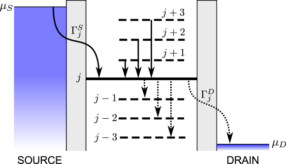
The processes that enter equation (16) are illustrated in figure 9. The first term on the r.h.s. describes the rate at which electrons tunnel from the S electrode. Due to the Coulomb blockade such a transfer is possible only when none of the DRN states is already occupied, what is ensured by the expression in parentheses. The second term describes relaxation to state from higher–lying states. The last term describes tunneling to the D electrode and relaxations from state to lower–lying states. If () the second (third) sum in equation (16) should be omitted since there are no states from (to) which relaxation is possible.
As we are interested in the steady–state current we put in equation (16). Then, introducing , the system of equations for can be rewritten as
| (24) | |||
| (43) |
In the absence of magnetic field is always equal to 1, but we have left it in the first row for consistency of notation.
The solutions can be easily found in limiting cases of a very slow relaxation and of a very weak couplings to the electrodes. In the former case, when we put for all and , the solution for a symmetric coupling () takes on a simple form . In the latter case, when we put for all , we get for all , what means that only the ground state participates in the transport. In a general case the system of linear equations (43) can be solved analytically, but with increasing the formulas quickly become very long. With the help of the occupation probabilities , the steady–state current can be expressed as a sum of currents carried by electrons which tunnel from the S electrode to all the states that lie in the bias window. Since in the steady state the currents through both the barriers are equal, the total current can be also expressed as a sum of currents carried by electrons which tunnel from the DRN to the D electrode. Then, the total current can be written as
| (44) |
where the currents carried by electrons tunneling to and from individual levels are given by
| (45) |
We assume, following the experiments in Refs. [10, 9], meV. Thus, in our studies both the energy spacings and the bias window are much larger than the thermal energy and we neglect the temperature smearing out of the energy levels. Then for a forward bias () the electrons can tunnel only from the S electrode to the DRN and then from the DRN to the D electrode. The tunnel rates in equation (43) depend on the DRN geometry. We assume it so that for the most strongly coupled state is equal to 5 GHz and calculate all the other couplings accordingly. That way all the tunnel rates are in the range of the experimentally accessible values [54].
We start with the low bias regime where only the ground state lies in the bias window (). In this case the total current is given by equation (45) with the requirement that :
| (46) |
We assume symmetric tunneling barriers to the S and D electrodes and numerically calculate their values. The mechanism of the SET is as follows: if the bottom of the QD potential is significantly below the bottom of the QR potential, the ground state is localized in the QD near the center of the DRN. Since for a deep enough QD potential the wave function decreases almost exponentially with increasing distance from the QD, its overlap with the electrode’s wave functions is negligible. With an increase of this state moves to the outer (QR) part of the structure where it has much larger overlap with the states in the electrodes. This results in a strong increase of the current. We calculate the current as a function of the gate voltage for three different values of . Results are presented in figure 10.
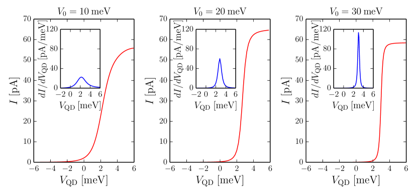
One can see in this figure that the steepness of the characteristics increases significantly with an increase of . If is small, the ground state wave function gradually moves with increasing towards the outer part of the DRN. This leads to a slow increase of the current. On the other hand, if is large, there are two pronounced minima of the confining potential (one in the QD and and one in the QR) and with increasing at some point the ground state wave function “jumps” from the QD to the QR. It results in a step–like characteristics. This dependence is clearly seen in the insets in figure 10, where the differential conductance is presented for different heights of the barrier separating the DRN.
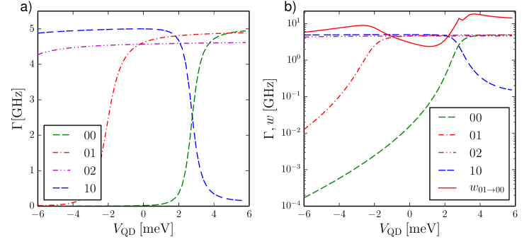
The low bias limit, however, not always can be reached. In many cases the evolution of the DRN’s spectrum shows several level crossings when is changed. In such cases the bias cannot be adjusted to include only the ground state for all values of for which the transistor effect occurs. We see in figure 2 that depending on two or three (or even more) states have to be accounted for. It is known that transport in the Coulomb blockade regime can be suppressed by the occupation of excited states [55]. Therefore, we analyze below how the system should be designed to get a good transistor behavior in the high bias regime. The dc currents are calculated as steady state solutions to the rate equations [equations (43-45)] for the occupation probabilities for all relevant states considering all the processes transferring electrons, namely the tunnel rates ’s and subsequent relaxation rates ’s. It turns out that the major factor that determines the current is the relations between the tunnel and relaxation rates. When the coupling to the electrodes is small compared to the corresponding relaxation rates, most of electrons that travel through the DRN will relax to the ground state before leaving the DRN by tunneling to the drain electrode. Then, the total current is determined mostly by the transport only through the ground state even if some of the excited states are in the bias window. In this case the system behaves like in the described above low bias limit. This situation is illustrated in figure 11.
What we have also noted from our numerical calculations is that if the relaxation rates ’s are comparable to the coupling constants ’s, then only a minor influence of higher excited states appears. They do not change the switching characteristics but increase the current amplitude.
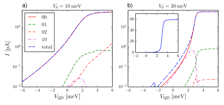
As follows from the calculations in Sec. 2.1 the relaxation rates are of the order of a few GHz in the broad range of . Therefore, one can easily obtain ’s smaller or comparable to the corresponding relaxation rates and consequently get the desired transistor behavior, as shown in the inset in figure 11b.
4 Current rectifier
Current rectification plays an important role in electron transport and is fundamental for the development of novel basic elements in nanoelectronics. The attempts have been made to build downscaled rectifiers. Coulomb blockade rectifier on a triple dot system [26, 56] has been recently introduced. Rectification properties of a quantum wire coupled asymmetrically to a quantum dot have also been studied [57]. We propose here a rectifier built on a DRN which utilizes different distribution of the ground and excited states wave functions.
To show the idea we discuss at first a case where the two lowest states are in the bias window and we present the analytical solutions for the currents.
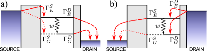
The confinement potential of the DRN is tuned so that the first excited state (E) has significantly larger overlap with the leads than the ground state (G). Thus, the same holds true for the corresponding tunneling rates, i.e, . To get current rectification we have to break the left–right symmetry, therefore we assume an asymmetric coupling to the source and drain electrodes, i.e., the drain electrode is much closer to the DRN than the source one. This results in the following relations between the tunneling rates:
| (47) |
where is assumed to be so small that the current between the ground state and the source electrode is negligible ( kHz [5]). One can tune the distances between the DRN and electrodes to ensure the above relation. Moreover, it follows from equations in the Appendix that the ratio of the tunneling rates to the ground and excited states is independent of this distance, so that
| (48) |
what is on line with the assumptions made, e.g., in Refs. [10, 54] in the interpretation of their experiments.
The proposed mechanism of the rectification is the following: for forward bias (, see figure 12a) the current from the source electrode flows to the DRN through the excited state and then either further flows to the drain electrode through the excited state or the electron relaxes and leaves the DRN through the ground state. This is the forward direction of the rectifier. On the other hand, for reverse bias (, see figure 12b) an electron can enter either the ground or the excited state. If the electron enters the ground state, it cannot leave the DRN because of the negligible coupling to the source electrode (we assume the temperature to be low enough to prevent from exciting the electron to the next energy level and from tunneling back to the drain electrode). If the electron enters the excited state, it will relax to the ground state due to fast relaxation (Sec. 2). Then, in either case the electron gets stuck in the ground state blocking the current through the excited state by means of the Coulomb blockade. This is the reverse direction of the rectifier.
To describe the proposed rectifier effect in a quantitative way we calculate the currents using the steady state solutions of the rate equations for the occupation probabilities [equations (43-45)]. Taking into account only the two lowest states we obtain the current for the forward bias and the reverse current for the reverse bias:
| (49) | |||||
| (50) |
where is the relaxation rate for the first excited state and is its degeneracy. These formulas allow us to find the conditions under which DRN behaves as a rectifier, i.e., for which
| (51) |
Since we get
| (52) |
One can see that the ratio of the forward and reverse currents depends crucially on the ratio between couplings of the ground and excited states to the S electrode and this is a parameter that can easily be tuned in a DRN.
We calculate the tunneling rates and and the relaxation rates as a function of under the assumption that the geometry of the DRN is that the maximal value of is 5 GHz.
Choosing meV (only two states in the bias window) for we get from equations (49), (50) and (52) fA, fA, what gives .
In this reference situation we get very small currents because both the G and E states are placed in the inner part of the DRN (see figure 3a). To get a stronger current we have to choose larger for which some excited states are placed in the outer part of the DRN resulting in the larger ratio of the respective tunneling rates . For meV we have to consider three states in the bias window, as can be infered from figure 2. Below we present two examples of our numerical results:
| wave functions | |||||
|---|---|---|---|---|---|
| 1 meV | 100 | 9 pA | 0.09 pA | 100 | figure 3b |
| 0 meV | 200 | 4 pA | 0.012 pA | 320 |
The wave functions in these two cases differ only qualitatively and therefore only the case of meV is presented in figure 3b. The above example illustrates that it is possible to design a DRN that allows one to get a substantial forward current and a high degree of rectification. The Coulomb blockade due to the electron stuck in the ground state will prevent from transport through any of the excited states in the reverse direction. On the other hand, they will all participate in the transport in the forward direction, what increases the total current. Because is not exactly equal to zero, we get some leakage current in the reverse direction but still substantial rectifying behavior occurs.
The crucial requirement for the rectifier is the strong difference between the coupling to the ground state and to the excited states. This is the point where the advantage of the DRN over a QD is clearly visible. We performed, for comparison, calculations for QD with nm, and have got in the most favorable case: pA, pA, . One cannot obtain here a high degree of rectification because it is impossible to change the relative distribution of the ground and excited state wave functions in a QD. As a result, one cannot decrease the current without simultaneous decreasing of . In QDs the ratio is usually below 10, whereas in the DRN the confining potential can be tuned to give up to . We see that the tunnel coupling to the reservoirs in the DRN is tunable over a much wider range than in QD. This, in turn, results in larger values of currents and more efficient rectification.
5 Summary
The fundamental requirement for future, low power consumption electronics is to control and manipulate single charges or spins. Quantum dots are the most popular and developed few–electron systems due to the relative easiness of fabrication and manipulation. On the other hand, the simple geometry of QDs allows modification of their electronic properties only to some extent, what encourages scientists to explore more complex systems like double or triple QDs. In this paper we performed systematic studies of electronic properties of a concentric dot-ring nanostructure and showed that, thanks to its non-trivial geometry, the structure offers unique possibilities to manipulate the electron wave functions. In particular, we have shown that by simple electrostatic gating one can move over the electron between the outer ring and the inner dot changing orbital relaxation by orders of magnitude and switching the character of a DRN from insulating to conducting. We have demonstrated that a DRN occupied by a single electron can be a good single electron transistor and a current rectifier with very high on/off ratio. The presented so called wave function engineering technique allows designing the properties of a system from the lowest quantum mechanical level. This is exactly how modern nanotechnology works and is the way to reach the limits of device miniaturization and to make the next step in development of quantum computers.
In the paper we present results for a DRN build as a InGaAs structure. However, the idea of a nanosystem where the wave functions can be moved over to different spatially separated parts can be applied also to other physical systems, for example graphene nanostructures [58, 59, 60, 61]. We also neglect the spin effects. Yet, exploiting them would allow one to use a DRN in nanospintronics. The effect of spin on the Coulomb blockade has been studied in single QDs [62, 55, 63, 5] and in double QDs [29, 64, 65]. A spin blockade in single electron transistor in QD resulting from spin polarized leads has been discussed in [66]. In the case of a DRN one would be able to independly control spin–up and spin–down quantum states, what would lead to spin dependent tunnel rates . This, in turn, would give the possibility to control a spin polarised current.
By studying one–electron properties we have demonstrated that the structure offers the unique possibilities to manipulate the distribution of the wave functions what influences different DRN features. It also provides great flexibility in manipulating many–electron states, what, however, is out of the scope of this paper and will be presented elsewhere.
Appendix A Derivation of the tunneling matrix element
According to Bardeen’s approach [48] the tunneling matrix element is given by
| (53) |
what in two dimensions can be written as
| (54) |
where is the DRN’s wave function and is the electrode’s wave function. The electrodes are modelled as half–planes and their wave functions and eigenenergies are given by
| (55) | |||||
| (56) |
where
| (57) | |||||
| (58) |
The wave function of the DRN can be written as
| (59) |
The derivatives in equation (54) are given by
| (60) |
and
| (61) |
For each in equation (53) one has to calculate and [equations (57) and (58)], insert equations (55), (59), (60), and (61) into (54) and (numerically) calculate the integral. It is convenient to express in polar coordinates where it takes the following form
| (62) | |||||
References
References
- [1] Kouwenhoven L, van der Vaart N, Johnson A, Kool W, Harmans C, Williamson J, Staring A and Foxon C 1991 Z. Phys. B Condensed Matter 85 367
- [2] van der Vaart N C, Godijn S F, Nazarov Y V, Harmans C J P M, Mooij J E, Molenkamp L W, and Foxon C T 1995 Phys. Rev. Lett. 74 4702
- [3] Devoret M H, Esteve D and Urbina C 1992 Nature 360 547
- [4] Kastner M A 1992 Rev. Mod. Phys. 64 849
- [5] Hanson R, Kouwenhoven L P, Petta J R, Tarucha S and Vandersypen L M K 2007 Rev. Mod. Phys. 79 1217
- [6] Blais A, Huang R S, Wallraff A, Girvin S M and Schoelkopf R J 2004 Phys. Rev. A 69 062320
- [7] Petta J R, Johnson A C, Taylor J M, Laird E A, Yacoby A, Lukin M D, Marcus C M, Hanson M P and Gossard A C 2005 Science 309 2180
- [8] Versteegh M A M, Reimer M E, Jöns K D, Dalacu D, Poole P J, Gulinatti A, Giudice A and Zwiller V 2014 Nature Communications 5298
- [9] Schleser R, Ruh E, Ihn T, Ensslin K, Driscoll D C and Gossard A C 2005 Phys. Rev. B 72 035312
- [10] Fujisawa T, Tokura Y and Hirayama Y 2001 Physica B 298 573
- [11] Amasha S, MacLean K, Iuliana P, Zumbühl D M, Kastner M A, Hanson M P and Gossard A C 2008 Phys. Rev. Lett. 100 046803
- [12] Fuhrer A, Lüscher S, Ihn T, Henzel T, Ensslin K, Wegscheider W and Bichler M 2001 Nature 413 822
- [13] Scheibner R, Koenig M, Reuter D, Wieck A D, Gould C, Buhmann H and Molenkamp L W 2008 New J. Phys. 10 083016
- [14] Lis K, Bednarek S, Szafran B and Adamowski J 2003 Physica E 17 494
- [15] Averin D V and Likharev K K 1986 Journal of Low Temperature Physics 62 345
- [16] Fulton T A and Dolan G J 1987 Phys. Rev. Lett. 59 109
- [17] Fujisawa T, Austing D G, Tokura Y, Hirayama Y and Tarucha S 2002 Nature 419 278
- [18] Koppens F H L, Buizert C, Tielrooij K J, Vink I T, Nowack K C, Meunier T, Kouwenhoven L P and Vandersypen L M K 2006 Nature 442 766
- [19] Elzerman J M, Hanson R, van Beveren L H W, Witkamp B, Vandersypen L M K and Kouwenhoven L P 2004 Nature 430
- [20] Weber C, Fuhrer A, Fasth C, Lindwall G, Samuelson L and Wacker A 2010 Phys. Rev. Lett 104 036801
- [21] Shinkai G, Hayashi T, Hirayama Y and Fujisawa T 2007 Appl. Phys. Lett 90 103116
- [22] McNeil R P G, Kataoka M, Ford C J B, Barnes C H W, Anderson D, Jones G A C, Farrer I and Ritchie D A 2011 Nature Letters 477 103116
- [23] Hatano T, Stopa M, Yamaguchi T, Ota T, Yamada K and Tarucha S 2004 Phys. Rev. Lett 93 439
- [24] Ota T, Ono K, Stopa M, Hatano T, Tarucha S, Song H Z, Nakata Y and Miyazawa T 2006 Nature 442 766
- [25] Koppens F H L, Buizert C, Tielrooij K J, Vink I T, Nowack K C, Meunier T, Kouwenhoven L P and Vandersypen L M K 2004 Phys. Rev. Lett 93 066801
- [26] Stopa M 2002 Phys. Rev. Lett. 88 146802
- [27] Vidan A, Westervelt R M, Stopa M, Hanson M and Gossard A C 2004 Appl. Phys. Lett 85 3602
- [28] Gaudreau L, Studenikin S A, Sachrajda A S, Zawadzki P, Kam A, Lapointe J, Korkusinski M and Hawrylak P 2006 Phys. Rev. Lett 97 036807
- [29] Ono K, Austing D G, Tokura Y and Tarucha S 2002 Science 297 1313
- [30] Johnson A C, Petta J R, Marcus C M, Hanson M P and Gossard A C 2005 Phys. Rev. B 72 165308
- [31] Zipper E, Kurpas M, Sadowski J and Maśka M M 2011 J. Phys. Condens. Matter 23 115302
- [32] Kurpas M, Zipper E and Maśka M M 2014 Engineering of electron states and spin relaxation in quantum rings and quantum dot-ring nanostructures Physics of Quantum Rings ed Fomin V M (Berlin, Heidelberg: Springer) p 455
- [33] Piacente G and Hai G Q 2007 Phys. Rev. B 75 125324
- [34] Lei W, Notthoff C, Lorke A, Reuter D and Wieck A D 2010 Appl. Phys. Lett 96 033111
- [35] Kleemans N A J M, Bominaar-Silkens I M A, Fomin V M, Gladilin V N, Granados D, Taboada A G, García J M, Offermans P, Zeitler U, Christianen P C M, Maan J C, Devreese J T and Koenraad P M 2009 Phys. Rev. Lett 99 146808
- [36] Aharonov Y and Bohm D 1959 Phys. Rev. 115
- [37] Büttiker M, Imry Y and Landauer R 1983 Phys. Rev. A 96 365
- [38] Bluhm H, Koshnick N C, Bert J A, Huber M E and Moler K A 2009 Phys. Rev. Lett. 102 136802
- [39] Birge N O 2009 Science 326 244
- [40] Somaschini C, Bietti S, Koguchi N and Sanguinetti S 2011 Nanotechnology 22 185602
- [41] Somaschini C, Bietti S, Koguchi N and Sanguinetti S 2010 Appl. Phys. Lett. 97 203109
- [42] Lauhon L J, Gudiksen M S, Wang D and Lieber C 2002 Nature 420 57
- [43] Dillen D C, Kim K, Liu E and Tutuc E 2014 Nature Nanotechnology 9 116
- [44] Szafran B, Peeters F M and Bednarek S 2004 Phys. Rev. B 70 125310
- [45] Zipper E, Kurpas M and Maśka M M 2012 New J. Phys. 14 093029
- [46] Kurpas M, Kędzierska B, Janus-Zygmunt I, Maśka M M and Zipper E 2014 Acta. Phys. Pol. A 126 A–20
- [47] Janus-Zygmunt I, Kędzierska B, Gorczyca-Goraj A, Kurpas M, Maśka M M and Zipper E 2014 Acta. Phys. Pol. A 126 1171
- [48] Bardeen J 1961 Phys. Rev. Lett. 6 57
- [49] Bockelmann U and Bastard G 1990 Phys. Rev. B 42 8947
- [50] Stano P and Fabian J 2006 Phys. Rev. B 74 045320
- [51] Hai G Q and Oliveira S S 2006 Phys. Rev. B 74 193303
- [52] Hanson R, Vink I T, DiVincenzo D P, Vandersypen L M K, Elzerman J M, van Beveren L H W and Kouwenhoven L 2004 Determination of the tunnel rates through a few-electron quantum dot Quantum Information and Decoherence in Nanosystems ed Glattli D C, Sanqeur M and Van J T T pp 145–150
- [53] Shavitt I 1977 Methods of Electronic Structure Theory (Plenum Press, New York) chap The Method of Configuration Interaction, pp 189 – 275
- [54] Fujisawa T, Tokura Y and Hirayama Y 2001 Phys. Rev. B 63 081304(R)
- [55] Weis J, Hang R H, v Klitzing K and Ploog K 1993 Phys. Rev. Lett. 71 4019
- [56] Yang C J and Gong W J 2013 J. Korean Phys. Soc. 63 1175
- [57] Mueller C R, Worschech L, Lang S, Stopa M and Forchel A 2009 Phys. Rev. B 80 075317
- [58] Molitor F, Güttinger J, Stampfer C, Dröscher S, Jacobsen A, Ihn T and Ensslin K 2011 Journal of Physics: Condensed Matter 23 243201
- [59] Stampfer C, Fringes S, Güttinger J, Molitor F, Volk C, Terrés B, Dauber J, Engels S, Schnez S, Jacobsen A, Dröscher S, Ihn T and Ensslin K 2011 Frontiers of Physics 6 271–293 ISSN 2095-0462
- [60] Trauzettel B, Bulaev D V, Loss D and Burkard G 2007 Nat Phys 3 192–196 ISSN 1745-2473
- [61] Ponomarenko L A, Schedin F, Katsnelson M I, Yang R, Hill E W, Novoselov K S and Geim A K 2008 Science 320 356–358
- [62] Johnson T, Kouwenhoven L P, de Jong W, de Vaart N C, Harmans C J P M and Foxon C T 1992 Phys. Rev. Lett. 69 1592
- [63] Weinmann D, Häsler W and Kramer B 1995 Phys. Rev. Lett. 74 984
- [64] Johnson A C, Petta J R, Markus C M, Hanson M P, and Gossard A C 2005 Phys. Rev. B 72 165308
- [65] Simmons C B, Koh T S, Shaji N, Thalakulam M, Klein L J, Qin H, Luo H, Savage D E, Lagally M G, Rimberg A J, Joynt R, Blick R, Friesen M, Coppersmith S N, and Eriksson M A 2010 Phys. Rev. B 82 245312
- [66] Ciorga M, Pioro-Ladriere M, Zawadzki P, Hawrylak P and Sachrajda A S 2002 Appl. Phys. Lett. 80 2177