Electron paths and double-slit interference in the scanning gate microscopy
Abstract
We analyze electron paths in a solid-state double-slit interferometer based on the two-dimensional electron gas and their mapping by the scanning gate microscopy (SGM). A device with a quantum point source contact of a split exit and a drain contact used for electron detection is considered. We study the SGM maps of source-drain conductance () as functions of the probe position and find that for a narrow drain the classical electron paths are clearly resolved but without any trace of the double-slit interference. The latter is present in the SGM maps of backscattering () probability only. The double-slit interference is found in the maps for a wider drain contact but at the expense of the loss of information on the electron trajectories. Stability of and maps versus the geometry parameters of the scattering device is also discussed. We discuss the interplay of the Young interference and interference effects between various electron paths introduced by the tip and the electron detector.
I Introduction
The scanning gate microscopy (SGM) is an experimental technique sgmr1 ; sgmr2 that probes transport properties of devices with the two-dimensional electron gas – buried shallow beneath the surface of the sample – by the charged tip of the atomic force microscope. The technique has been used in particular for investigation of quantum point contacts – the most elementary quantum transport devices topinka1 ; topinka2 . The conductance maps gathered with the SGM contain characteristic oscillation of the period of half the Fermi wavelength that appear due to the interference of electron wave functions incoming from the quantum point contact and backscattered by the tip int1 ; int2 ; int3 ; int4 ; Jalabert2010 ; Gorini2013 ; Brun2014 ; kozikov2013 ; paradiso . In our recent paper Kolasinski2014 we have proposed a system with split source channel for observation of the double-slit interference. The Young interference should be present in the SGM maps provided that the transport in the channel which feeds the split source occurs in the lowest subband of lateral the quantization Kolasinski2014 . The proposal of Ref. Kolasinski2014 and most of the experimental studies int1 ; int2 ; int3 ; int4 dealt with systems in which the electron after passing through the constriction defining the quantum contact enters an infinite half-plane. In this work we consider the possibility of observation of electron paths in the context of the double-slit interference. According to the which-path thought experiment by Feynman Fey determination of the slit the electron goes through destroys the double-slit interference. Here, we demonstrate that SGM can be used for detection of classical electron paths – although without indicating the one taken by the electron – with a simultaneous resolution of the double slit interference effects. The SGM was early used for detection of the semi-classical electron trajectories as deflected by the Lorentz force crook , including observation of the skipping orbits skipping ; aidala for systems with an additional confinement. Observation of electron paths requires placing an electron detector in the system – usually another QPC serving as the drain channel crook ; skipping ; aidala . In the present paper we consider a system with a split QPC serving as the electron source and the second QPC used for detection of the electron passage. We demonstrate that the source-drain conductance maps for a narrow drain detector indicate the classical paths but miss the double-slit interference. For enlarged drain width the double-slit interference appears in the map but the image of the paths is lost. The simultaneous observation of both the semi-classical paths and the Young interference is possible when besides the map of source-drain conductance one considers the SGM maps for backscattered electrons – or equivalently – the maps for conductance between the source and the rest of the system excluding the drain detector. We also discuss the electron paths in terms of the quantum consequences in various interference effects. In particular we also point out that backscattering by the tip induces interference between the slits with a characteristic SGM pattern that is superimposed on the Young interference image.
II Model
 |
 |
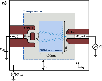
We consider an experimental situation that is depicted in Fig. 1(a). The current is fed by the source contact to the channel that is filtered by the split quantum point contact QPC1. The second QPC (QPC2) serves as an entrance to the drain contact at the right side of the figure that will be used for electron detection as in Refs. crook ; aidala ; skipping or more recently in Ref. khatua2014 . The effective width of the source channel and the width of both slits at the QPC1 side is taken equal 40 nm, which for the considered Fermi energy transmits the current in the lowest subband only. According to the previous paper Kolasinski2014 the lowest subband transport on the input part is necessary for the Young interference to be observed. For a larger number of incident subbands the conductance map for the double slit system is a simple sum of maps for separate QPCs Kolasinski2014 since the double-slit interference disappears in the Landauer summation over the incident subbands. The electron leaving QPC1 enters a finite but large sample filled by 2DEG. By large we mean that the distance between the region of interest for the SGM and the edges of the sample is larger than the coherence length, so that the interference with the edges can be neglected. The source-drain voltage is considered low enough for the linear transport conditions to occur. The current passing to the drain is measured in order to evaluate the conductance. The sample is grounded by a large reflectionless contact and this current is measured to evaluate the leakage conductance . From conservation of the current and for subband in the input channel (we consider mostly ) we have
| (1) |
where , where is the backscattering probability. Thus, can be determined when and are measured. In the following we discuss numerical results for and .
In the calculations we focus on the region marked by the dashed lines in Fig. 1(a). We assume that the transport is coherent within the computational box. At the dashed lines we apply transparent boundary conditions, so that the region of interest is effectively open, in contrast to systems with a pair of QPCs used as source and drain for a closed stadium that are studied by SGM in e.g. Refs. kozikov ; kozikov2 . In this paper we set the distance between the input slits nm, which is large enough to distinguish trajectories of the electron arriving to QPC2 from one of the input slits. In Fig. 1 a smaller value of nm is used for illustration. The total computational box covers the region where the transparent boundary conditions are applied of size 800nm1000nm and the region where the scans by the SGM are taken is significantly smaller: 400nm 600nm – see Fig. 1(a).
In order to simulate the propagation of the Fermi level electrons within the region inside the computational box (dashed lines in Fig. 1(a)) we consider coherent transport as described by the effective-mass Schrödinger equation,
| (2) |
where is GaAs electron effective mass, is the Fermi level energy, and potential
| (3) |
describes the effective perturbation induced by the AFM tip with amplitude meV and width , localized above point . This type of effective Lorentzian-shaped perturbation, which results from the screening of the charge on the tip by the 2DEG electron gas located under the sample surface, was obtained previously in our self-consistent Schrödinger-Poisson calculations kolasinski2013 ; szafran . The width of the potential is of the order of the distance between the tip and the 2DEG szafran . In the SGM experiments the 2DEG is buried at least 25 nm below the surface atleast , and the minimal distance of the tip to the surface applied in SGM is 20 nm sgmr1 , hence a minimal realistic value of is about 50 nm. In this paper we consider two widths of the tip: a small one nm which is useful for the initial discussion since it sets the precision of the determination of electron paths, and a realistic one – nm.
For simplicity in order to define the contacts we assume hard-wall boundary conditions on QPC1 and QPC2. In experimental setups the QPCs are usually defined electrostatically by potential applied between the gates so that the QPC potential has a saddle point profile. Nevertheless, we do not discuss conductance quantization as function of the QPC width and for a fixed number of transmitting subbands the hard-wall potential gives qualitatively similar results to a saddle point potential which was applied in a previous work Nowak2014 . The transparent boundary conditions at the blue dashed line of Fig. 1(a)) were introduced by the method described in Ref. Nowak2014 .
We work within the Landauer approach for a zero temperature in the finite difference implementation Kolasinski2014QHI of the quantum transmitting boundary method Lent90 ; Lent94 . Within the input channel – before the splitting ending with the two QPC1 slits, the wave function at the Fermi level is given by the superposition of incoming and backscattered transverse modes
| (4) | |||||
where the last term corresponds to the summation over the evanescent modes Lent90 ; Lent94 ; Bagwell1990 and is the number of current propagating transverse modes in QPC1. We consider a single subband in the QPC1 channel and an arbitrary number of subbands in the QPC2 channel. The summation runs over the Fermi level wave vectors at subsequent lateral subbands. The transport from the input channel to the two-slits is non-adiabatic with a pronounced backscattering. Note, that the central island [Fig. 1(a)] used as a beam splitter in the presence of a strong external magnetic field is likely to form a quantum Hall interferometer as discussed in Refs. ensliny ; martinsy
For QPC2 we assume the boundary conditions of form
| (5) | |||||
with being the number of conducting transverse modes in QPC2. The transverse modes for both QPCs were calculated using the method of Ref. Zwierzycki2008 . The scattering amplitudes and the amplitudes of the incoming modes of Eq. (4) once established are used to calculate the transmission probabilities. Throughout this paper we keep meV which gives the value of nm. We choose discretization grid spacing nm, which is small compared to .
After solution of Eq. 2 for each incoming mode the source-drain conductance is evaluated from the Landauer formula
| (6) |
where is the transmission probability of the -th mode incoming from the QPC1 to the QPC2 and . We refer to the sum of backscattering probabilities as the ”resistance”, which is given by the formula
| (7) |
where is the backscattering probability of -th incoming mode to the QPC1.
We discuss below the maps of backscattering probability (SGM-R) and conductance maps (SGM-G) for current flow between QPC1 and QPC2. In order to calculate the SGM-R/G images we evaluated the ”resistance” R and conductance G by scanning the system with the tip potential given by Eq. (3) inside the rectangle shown in Fig. 1(b). The spacing between two subsequent positions of the tip was nm, thus in order to obtain the SGM image, presented later in paper, for the scan area 400nm 600nm one has to solve the scattering problem 15000 times.
III Results and discussion
III.1 In the absence of the tip: Young interference and interference due to QPC2 detector
We begin the discussion by setting equal widths of both input and output channels within QPCs, nm. In both the input and the output channels we have a single subband transport for the applied Fermi energy of meV. According to our previous paper Kolasinski2014 the single subband transport on the input part allows for resolution of the Young interference pattern by the SGM technique.
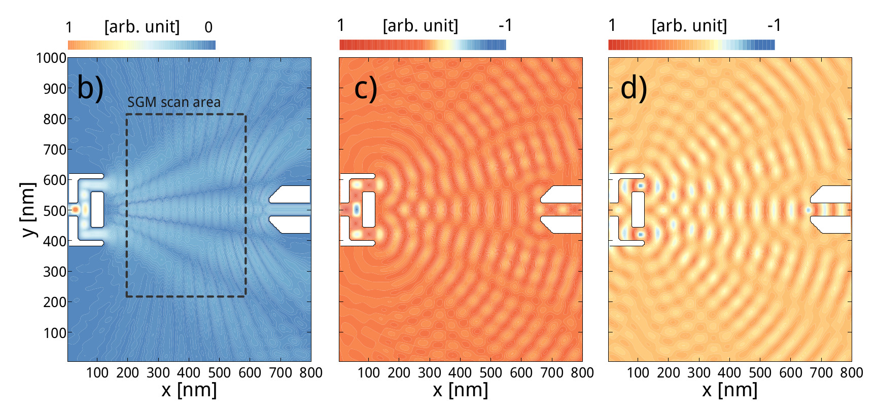
The amplitude of the scattering wave function in the absence of the tip is shown in Fig. 1(b). Besides the well-resolved Young interference pattern with five more or less straight lines of constructive and destructive interference for the waves passing through both the slits [see Fig. 2(c)] one also notices additional vertical interference fringes. This feature is caused by the presence of the output QPC2 which reflects the incoming wave function back to the double slit device.
The role of QPC2 in the scattering is more clearly visible in the real part of the wave function displayed as Fig.1(c). We found that a very similar wave function can be reproduced by a superposition of three point sources positioned at the center of each slit of the system following the Huygens–Fresnel principle for the circular waves propagating from the input slits and QPC2 – the latter as due to backscattering of the incoming wave Gorini2013 . In the limit of thin slit the Fermi level wave function at position traveling from the slit located at position can be well described by the angle-modulated Henkel function
| (8) |
where is angle between vector and the axis, i.e. and is a scattering amplitude. For the superposition of the three point sources one has
| (9) | |||||
where , and are the positions of slits in the system of Fig. 1(b). We set , for which we get the best agreement with the exact solution obtained from Eq. (2). The real part of the wave function obtained from Eq.(9) is plotted in Fig. 1(d). Note that the fitted value of is quite large, which suggests that the backscattering from QPC2 will have a substantial influence on the SGM images discussed below.
III.2 Interference mechanisms due to the tip
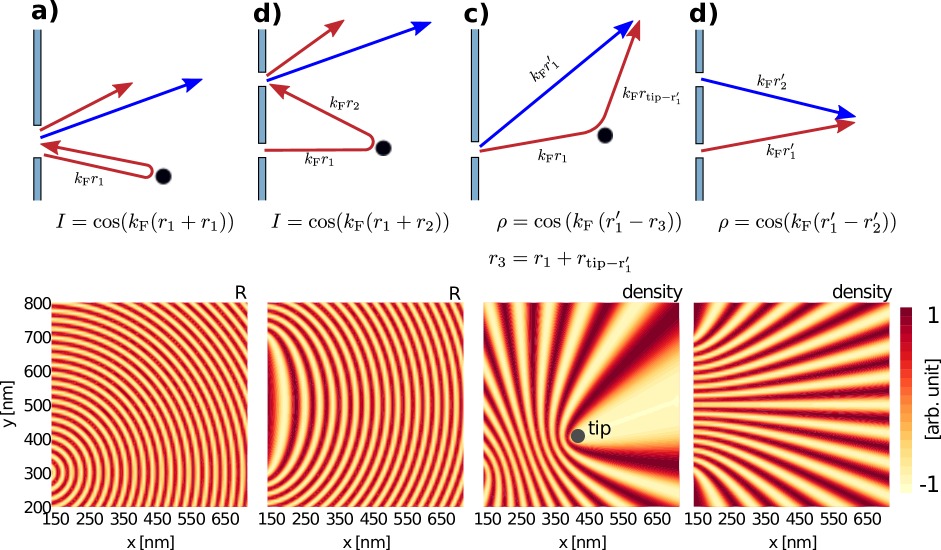
The backscattering by the tip introduces additional interference effects which will be discussed below: with the electrons reflected to the source QPC [Fig. 2(a)], the tip-induced double slit interference [Fig. 2(b)] and the interference of the direct wave with the scattered one [Fig. 2(c)]. The conductance map fringes due to the scattering of the type given by Fig. 2(a) is well known and has been discussed in a number of papers int1 ; int2 ; int3 ; int4 ; Jalabert2010 ; Gorini2013 ; Brun2014 ; kozikov2013 . The backscattering () is enhanced when the phase shift of the wave going to the tip and back [red arrows in Fig. 2(a)] produces a constructive interference with the incident wave [blue arrow in Fig. 2(a)] at the input slit. The signal is then proportional to
| (11) |
where in the argument is the phase acquired by the electron wave function on its way from a slit of QPC1 to the tip and back from the tip to the same slit. The interference of Fig. 2(a) leads to the angle-independent modulation of the maps which oscillate as a function of distance from the slit with the period of half the Fermi wavelength Jalabert2010 ; Gorini2013 .
The tip induces a double-slit interference of the wave passing through one of the slits of QPC1 and scattered by the tip with the wave incident from the other QPC1 slit [Fig. 2(b)]. Then, an enhanced backscattering can be expected when the interference of the incident and returning path is positive, or the signal will be proportional to
| (12) |
The result of formula (12) is plotted in Fig. 3(g), with a good agreement with the oscillations found in the results of the scattering problem of Fig. 3(e-f). The double slit interference according to mechanism of Fig. 2(b) and the resulting SGM effects were never discussed before. The equations (11 and 12) produce the same periodicity of at a large distance from QPC1.
The tip induces also interference of the waves incident from one of the QPCs and backscattered by the tip – as depicted in Fig. 2(c). The modulation of the scattering density for a fixed tip position is given by
| (13) |
with , and is the distance between the tip and . The results of Eq. 13 are displayed in the lower panel of Fig. 2(c) for a given tip position. This type of interference leads to lateral fringe patterns in SGM-G images to be discussed below.
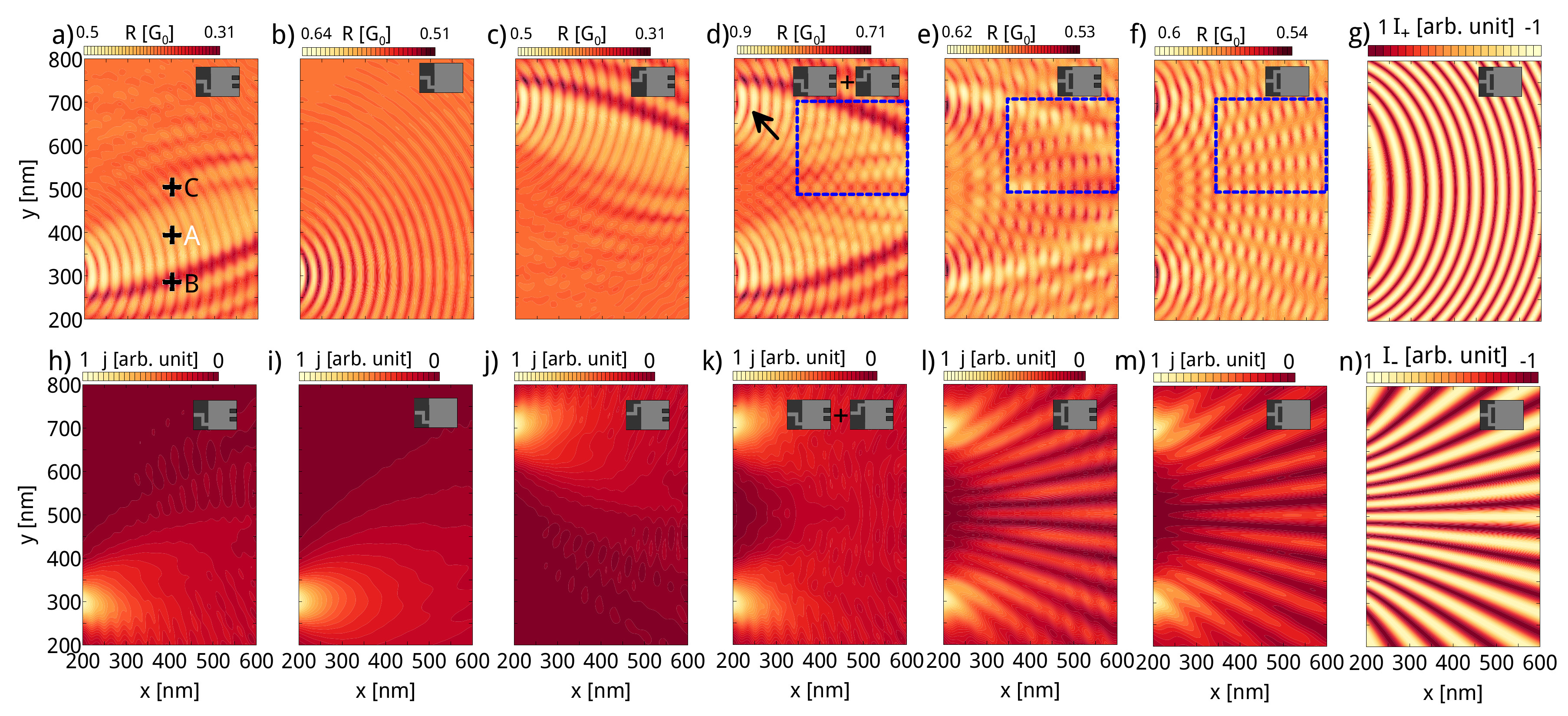
III.3 Resistance maps
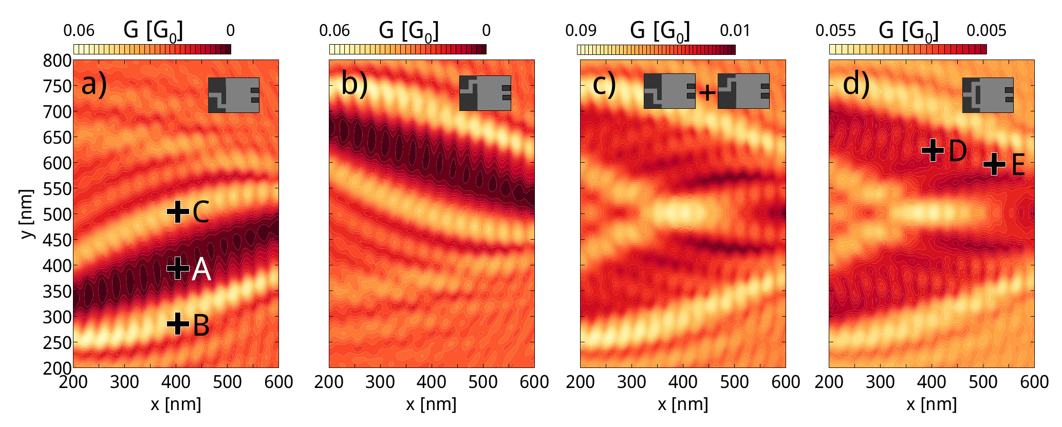
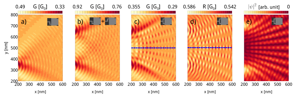
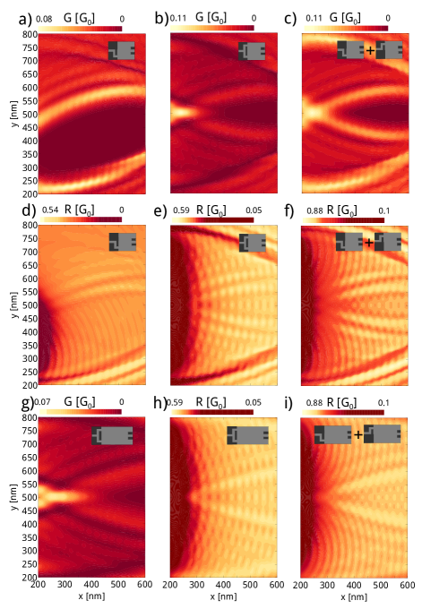
In Fig. 3(a-f) we show the SGM maps of resistance (SGM-R) as functions of the position of the AFM tip. The area of the scan is shown by the blue rectangle in Fig. 1(a,b). We consider a single or both QPC1 slits open as illustrated schematically in the insets in the top-right corner. For each system we plotted in the second row [Fig. 3(h-m)] the corresponding probability current distribution. In Fig. 3(a,b) we show the results of SGM-R images obtained for a single (lower) input slit open. In the absence of QPC2 [Fig. 3(b)] we observe circular fringes in the SGM map due to the interference of type given by Fig. 2(a) between the wave incoming from the slit and the wave backscattered by the AFM tip [see the arrow in Fig. 3(d), Fig. 2(a), and Eq. 11].
Figure 3(d) presents the sum of SGM-R maps of Fig. 3(a) and (c) obtained for a single slit open. The sum is quite different from the image obtained for the system where both the QPC1 slits are open (see Fig. 3(e)), which is a signature of the double-slit interference effects, and involve both the Young interference [Fig. 2(d)] and the tip-induced interference [Fig. 2(b)]. The Young interference is more clearly resolved in the absence of QPC2 [Fig. 3(f)], although it is also present when the QPC2 detector is a part of the setup [Fig. 3(e)]. In order to demonstrate this closer we extracted the enlarged fragments of Fig. 3(e,f) in Fig. 4(b,c). For a simple sum of SGM images for separate slits [Fig. 3(d)] instead the elliptic fringes or Young pattern we observe a checkerboard pattern [Fig. 3(d) and Fig. 4(a)]. This checkerboard pattern should be observed in the experiments for a large number of incident subbands, i.e. at higher Fermi energy or wider input channel as discussed in Ref. Kolasinski2014 .
In Figs. 3(h-m) we plotted the current density within the system in the absence of the tip. Note, for the double slit systems [Fig. 3(l,m)] that the current distribution is very similar with or without QPC2. The deformation of the Young interference for the system with QPC2 is due to the lateral interference pattern involving the paths marked in Fig. 2(b) which are introduced by QPC2.
The Young interference pattern given by Eq. (10) and calculated for the Fermi wave vector is displayed in Fig. 3(n) with a good agreement with the probability current distribution of Fig. 3(l,n) and the features of the SGM map of Fig. 3(f). A resemblance to Fig. 3(e) – for QPC2 present – can also be spotted, although the lines of flat in Fig. 3(e) are curved. The curvature as well as the presence of the lateral fringes can be reduced by placing the QPC2 further from QPC1, thus reducing the backscattering by QPC2 but at the expense of the reduced map contrast (see below).
III.4 Source-drain conductance maps
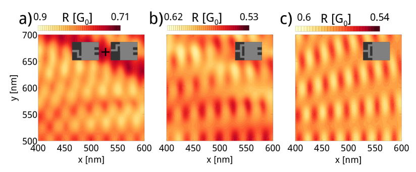
The SGM maps of source-drain conductance (SGM-G) of Fig. 5 exhibit a valley of minimal values along the shortest path from the source channel to the drain. The pattern of the image obtained for both slits open [Fig. 5(d)] is exactly the same as the one given by the sum of images Fig. 5(a) and (b) (see Fig. 5(c)). This shows that in SGM-G images the double-slit interference is absent, which may be quite surprising, given that the SGM-R image clearly resolved the interference.
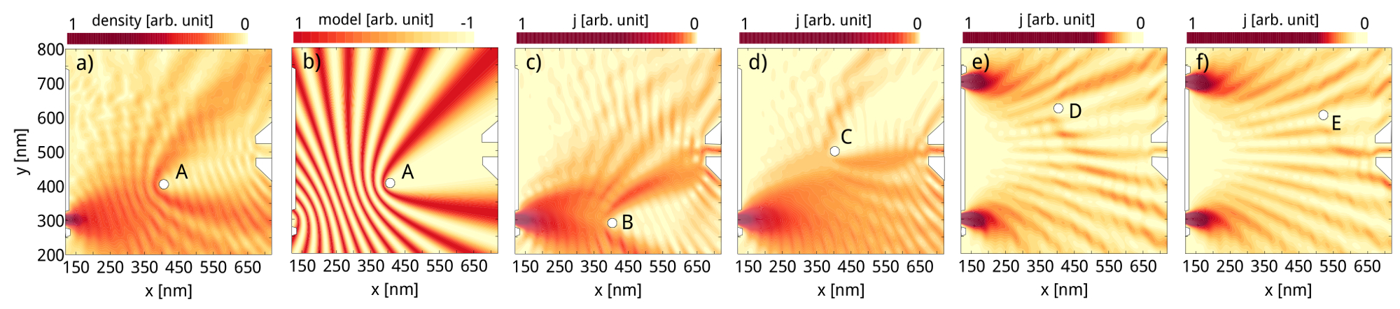
In Fig. 5(a) a lateral fringe pattern is observed along the classical trajectory. This valley of minimal values coincides with the line of maximal backscattering observed in Fig. 3(a). Figure 6(a) shows that the tip separates the electron wave into beams, which arise from the interference of waves incoming from QPC1 and scattered by the tip – as illustrated by Fig. 2(c). The variation of the electron density can be approximated by Eq. 13. The results of formula (13) are plotted in Fig. 6(b) with a very good agreement with the numerical result of Fig. 6(a), which however contains also the fringes due to backscattering by QPC2. Figure 6(a) corresponds to the position of the tip above the point A and explains the valley of low conductance in the SGM-G image (e.g. see Fig. 5(a)), since QPC2 is in the shadow cast by the tip. Figures 6(c-d) correspond to tip above points B and C for a single slit and explain the increase in the conductance around the classical path, which is well visible in Fig. 5(a) and (b). If we move the tip to positions B or C (see Fig. 6(b) and (c)) the electron wave is still separated into two main beams with one of these beams reaching QPC2, which produces the characteristic envelope of high conductance around the “classical path”. The minima of the lateral pattern of Fig. 5 appear when a nodal line of the interference passes to the QPC2 detector.
The points in Fig. 3(a) are the same as in Fig. 5(a) and correspond to plots Fig. 6(a-d). Note that point corresponds to a minimum of and maximum of , while point corresponds to a maximum of both quantities. The lateral pattern in the map appears only in presence of QPC2 detector [cf. Fig. 3(a) and Fig. 3(b)], and is a result of scattering first by the tip and next by QPC2. The effect of the interference of type Fig. 2(b) depends on the 1) position of the tip with respect to QPC2 - QCP1 – return path for the backscattered electrons and 2) the incidence angle of the waves deflected by the tip on the edges of the QPC2 electron.
Let us now consider both slits open with the AFM tip at position where the electron flow from the upper slit is totally blocked (see Fig. 6(e)). The current flux from the lower slit will be the only one reaching the QPC2. The tip in this manner turns off one of the slits of the source channel. Using the symmetry arguments for the considered device we will get the same conclusion with second slit blocked and the first transmitting current. Such argumentation can explain why at certain points in the obtained SGM-G maps there is no visible interference. Nevertheless, there are points where the potential of the tip does not totally block the current from any slit, so an interference could be expected. Such a case is presented in Fig. 6(f), with the tip located at a position where the current distribution is almost the same as in the unperturbed system (for comparison see Fig. 3(l)). We conclude that the double-slit interference is clearly visible in the current distribution but not in the SGM-G images.
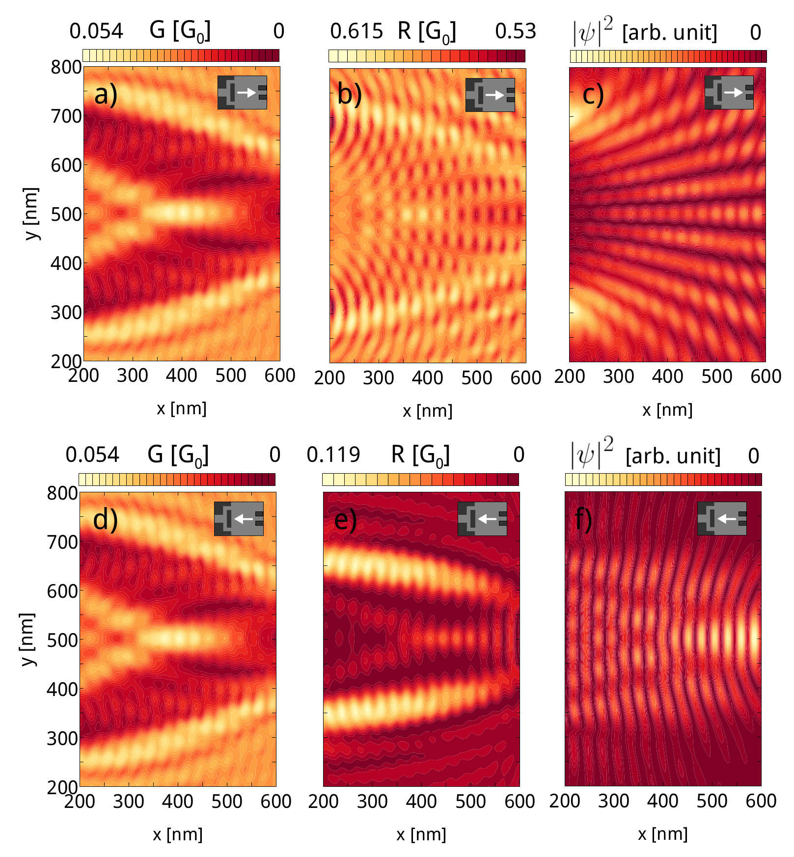
The lack of Young interference in the source-drain conductance images can be explained using a reversed bias and the current flowing in the reverse direction, i.e. from QPC2 to QPC1. The upper row of Fig. 7 shows the SGM-G, SGM-R and probability density for the current flowing from the double slit to QPC2, while the lower presents the quantities for the opposite current direction. We can see that the results for SGM-G are exactly identical for both current directions [Fig. 7(a,d)] in spite of the fact that the electron scattering is very different in both setups with a clear Young interference in Fig. 7(c) with no similar counterpart in Fig. 7(f).
The SGM-G images for both the cases [Fig. 7(a,d)] is bound to be identical due to the Onsager microreversibility relation for the single subband transport , which in terms of the Landauer approach implies no current flow for zero bias. For the electron incident from the right there is no reason to expect a presence of the Young interference, which is indeed missing in Fig. 7(f). The absence of the double slit interference in SGM-G follows from this observation and the microreversibility relation. Note, that SGM-R image for the reversed current orientation [Fig. 7(e)] clearly indicates the classical paths that the electron can follow from QPC2 to QPC1. Note, that QPC2 is further 100 nm to the right of the end of the figure and that two bright beams are emitted from QPC2 which is only 40 nm wide.
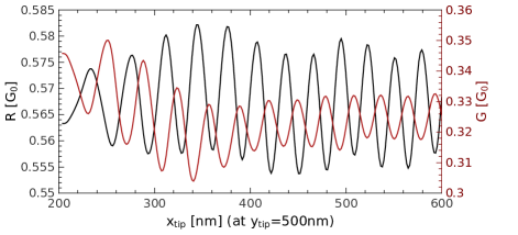
There is a way to restore the interference in the SGM-G images. Each of the subbands is with a certain probability backscattered, transferred to QPC2 or goes out of the computational box through the transparent boundary conditions to the rest of the system [see Eq. (1)] and is independent of the tip position. Now if we consider that becomes wider, the ratio decreases, since QPC2 will be able to transfer more current and the probability of the electron transfer form QPC1 to QPC2 increases with the width of the latter. Thus for a large width the value of in Eq. (1) will be small and hence . We can express the conductance of the system in as . We can see that for large values of the SGM-G should start to exhibit the interference pattern as the SGM-R images do. In Fig. 8(a-e) we show the results obtained for a large value of QPC2 width nm. Fig. 8(a) shows the SGM-G image for the bottom slit open, and Fig.8(b) is a sum of the images obtained for bottom and upper slit open separately. Now, the SGM-G image for both slits open (Fig. 8(c)) is clearly different from Fig. 8(b) with distinct stripes due to the Young interference. We can compare this result with SGM-R image of Fig.8(d) which is now quite similar to the SGM-G image, particularly in the center and close to QPC2. In this region the approximated relation is well visible and SGM-G image is indeed a negative of SGM-R image. To illustrate this further in Fig. 9 we plotted cross section of these images along the axis of the device.
Note that the increased width of QPC2 allows us to restore the interference in the SGM-G images, but at the expense of the lost information on the electron trajectories from QPC2 to QPC1. The double-slit interference is present as long as one does not interfere with the measurement trying to determine through which slit the particle passes Fey . Here, if we set the detector (QCP2) for mapping the electron trajectories – with a small value of – we gain the information about electron trajectories, but we lose the interference pattern. Increasing the width leads to reduction of spatial resolution of the detector, so we lose the paths in the images but restore the interference pattern.
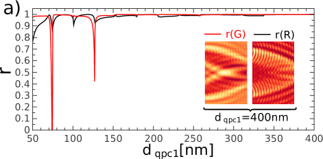
III.5 Stability of classical trajectories in SGM-G images
The classical trajectories as extracted from the SGM-G images should be stable against the geometrical parameters of the system, the distance between the QPC1 slits in particular. For each value of the interslit distance we calculated the SGM-G() and SGM-R() images. The calculations were performed for nm. In Fig. 10(a) we plotted the Pearson correlation coefficient kolasinski2013 between SGM-G() and last image SGM-G(400nm) – the curve, and correlation between SGM-R() and SGM-R(400nm) – the curve. We chose the SGM image for nm as a reference one. One may see in Fig. 10(a) that both lines and quickly stabilize around 1 after nm, which means that through all the values from around nm to 400nm both images stay almost unchanged. Note, that the double-slit interference in SGM-R images is only well resolved for the lowest subband transport in the incident channel Kolasinski2014 .
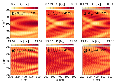
We found that the SGM-G images are generally stable in function of , which means that paths are always visible, but there is one exception when the distance between slits is small enough such that both trajectories (from each QPC) overlap which makes the calculated SGM-G maps difficult to interpret. Sample images of SGM-G and SGM-R for small value of nm are displayed in Fig. 10(b) and (e), respectively. For larger values of the classical trajectories are restored (see Fig. 10(c) and (d)). Note that for Fig. 10(c) and (d) the difference between the values of in each case is equal to 16 nm. The results for SGM-G are nearly identical. However, the SGM-R images – sensitive to the interference effects – very strongly depend on a specific value of – cf. Fig. 10(f) and (g). The wave function passing through both the input slits interferes with the AFM tip, as well as with QPC2. The result of the interference in terms of the backscattering depends on the variation of the distance between the slits of the order of the period of the waves formed by interference at the Fermi level which is equal to .
III.6 Wide tip potential
Let us return to the single subband transport in the input and the output leads and consider the wider tip potential nm. The results for conductance for a single slit – Fig. 11(a) and both the slits Fig. 11(b) still indicate the classical current paths, although naturally the width of the minima is significantly increased. The map pattern is still very similar to the one obtained by a sum of maps for separate slits [Fig. 11] - indicating a lack of double slit interference features in the source-drain conductance maps for , as discussed above.
The ”resistance” map [Fig. 11(e)] for both QPC1 slits open contains i) the circular fringes near the input slits [single slit interference of Fig. 2(a)], ii) elliptical fringes [double slit interference of Fig. 2(d)], iii) the lateral fringes [Fig. 2(b)]. All the effects (i-iii) are tip-related and in this case dominates the Young interference – which is weaker although still detectable. The Young interference is restored when the QPC2 detector is placed further from the QPC1 [see Fig. 11(h)], but naturally at the expense of the amplitude of the signal [Fig. 11(g)]. The reduction of the lateral fringe pattern is observed for – since it involves backscattering by QPC2 – is also observed [Fig. 11(h-i)].
IV Conclusions
We have considered imaging of electron trajectories for the double-slit experiment with the SGM technique. Several interference mechanisms induced by the tip and the drain contact as the electron detector have been found and the paths leading to the interference have been identified. We studied the SGM source-drain conductance maps and demonstrated that the classical electron paths are clearly resolved but only for a narrow drain contact, for which the double-slit interference features are absent. The double-slit interference pattern is present in the conductance maps but only for a wider drain contact, when the electron paths are no longer resolved.
We have indicated that a way to observe both trajectories and interference pattern is to look simultaneously at two different SGM maps – for the backscattering – which contain double-slit interference signal and for the conductance – that reveals the paths. The latter allows one to map all the equivalent classical trajectories, but without indicating the specific path the electron took on its way to the drain channel.
Acknowledgments This work was supported by National Science Centre according to decision DEC-2012/05/B/ST3/03290, and by PL-Grid Infrastructure. The first author is supported by the scholarship of Krakow Smoluchowski Scientific Consortium from the funding for National Leading Reserch Centre by Ministry of Science and Higher Education (Poland).
References
- (1) H. Sellier, B. Hackens, M.G. Pala, F. Martins, S. Baltazar, X. Wallart, L. Desplanque, V. Bayot, and S. Huant, Sem. Sci. Tech. 26, 064008 (2011).
- (2) D.K. Ferry, A.M. Burke, R. Akis, R. Brunner, T.E. Day, R. Meisels, F. Kuchar, J.P. Bird, and B.R. Bennett, Sem. Sci. Tech. 26, 043001 (2011).
- (3) M. A. Topinka, B. J. LeRoy, S. E. J. Shaw, E. J. Heller, R. M. Westervelt, K. D. Maranowski, and A. C. Gossard, Science 289, 2323 (2000).
- (4) M. A. Topinka, B. J. LeRoy, R. M. Westervelt, S. E. J. Shaw, R. Fleischmann, E. J. Heller, K. D. Maranowski, and A. C. Gossard, Nature 410, 183 (2001).
- (5) A. Cresti, J. Appl. Phys. 100, 053711 (2006).
- (6) M.P. Jura, M.A. Topinka, L. Urban, A. Yazdani, H. Shtrikman, L.N. Pfeiffer, K.W. West, and D. Goldhaber-Gordon D, Nat. Phys.3, 841 (2007).
- (7) M. P. Jura, M. A. Topinka, M. Grobis, L. N. Pfeiffer, K. W. West, and D. Goldhaber-Gordon, Phys. Rev. B 80, 041303(R) (2009).
- (8) A. Abbout, G. Lemarie, and J.-L. Pichards, Phys. Rev. Lett. 106, 156810 (2011).
- (9) R. A. Jalabert, W. Szewc, S. Tomsovic, and D. Weinmann, Phys. Rev. Lett. 105, 166802 (2010).
- (10) C. Gorini, R. A. Jalabert, W. Szewc, S. Tomsovic, and D. Weinmann, Phys. Rev. B 88, 035406 (2013).
- (11) B. Brun, F. Martins, S. Faniel, B. Hackens, G. Bachelier, A. Cavanna, C. Ulysse, A. Ouerghi, U. Gennser, D. Mailly, S. Huant, V. Bayot, M. Sanquer, and H. Sellier, Nat. Commun. 5, 4290 (2014)
- (12) A. Kozikov, D. Weinmann, C. Rössler, T. Ihn, K. Ensslin, C. Reichl, and W. Wegscheider, New J. Phys. 15, 013056 (2013).
- (13) N. Paradiso, S. Heun, S. Roddaro, L.N. Pfeiffer, K.W. West, L. Sorba, G. Biasiol, F. Beltram, Physica E 42, 1038 (2010)
- (14) K. Kolasinski, B. Szafran, M. P. Nowak, Phys. Rev. B. 90, 165303 (2014)
- (15) R.P. Feynman, Robert B. Leighton, and Matthew Sands The Feynman Lectures on Physics, Vol. 3., Addison-Wesley (1965); R. Bach, D. Pope, S.H. Lou, and H. Batelaan, New J. Phys. 15, 033018 (2013).
- (16) R. Crook, C.G. Smith, M.Y. Simmons, and D.A. Ritchie, Phys. Rev. B 62, 5174 (2000).
- (17) K. E. Aidala, R. E. Parrott, T. Kramer, E. J. Heller, R. M. Westervelt, M. P. Hanson, and A. C. Gossard, Nat. Phys. 3, 464 (2007).
- (18) K. E. Aidala, R. E. Parrott, E.J. Heller, and R.M. Westervelt Physica E, 34, 409 (2006).
- (19) P. Khatua, B. Bansal, and D. Shahar, Phys. Rev. Lett. 112, 010403 (2014)
- (20) A. Kozikov, D. Weinmann, C. Rössler, T. Ihn, K. Ensslin, C. Reichl, and W. Wegscheider, New J. Phys. 15, 083005 (2013).
- (21) A. Kozikov, R. Steinacher, C. Rössler, T. Ihn, K. Ensslin, C. Reichl, and W. Wegscheider, New. J. Phys. 16, 053031 (2014).
- (22) K. Kolasiński, B. Szafran Phys. Rev. B 88, 165306 (2013)
- (23) B. Szafran, Phys. Rev. B 84, 075336 (2011)
- (24) N. Pascher, F. Timpu, C. Rössler, T. Ihn, K. Ensslin, C. Reichl, and W. Wegscheider, Phys. Rev. B 89, 24508 (2014).
- (25) F. Martins, S. Faniel, B. Rosenow, M. G. Pala, H. Sellier, S. Huant, L. Desplanque, X. Wallart, V. Bayot, and B. Hackens, New J. Phys. 15, 013049 (2013).
- (26) B. Hackens, F. Martins, S. Faniel, C. A. Dutu, H. Sellier, S. Huant, M. Pala, L. Desplanque, X. Wallart, V. Bayo, Nature Commun. 1, 39, (2010)
- (27) M. P. Nowak, K. Kolasinski, B. Szafran, Phys. Rev. B 90, 035301 (2014)
- (28) K. Kolasinski, B. Szafran, Phys. Rev. B 89, 165306 (2014)
- (29) D. J. Kirkner and C. S. Lent, Journal of Applied Physics 67, 6353 (1990)
- (30) M. Leng and C. S. Lent, Journal of Applied Physics 76, 2240 (1994)
- (31) P. F. Bagwell, Phys. Rev. B 41, 15 (1990)
- (32) M. Zwierzycki, P. A. Khomyakov, A. A. Stariko K. Xia, M. Talanana, P. X. Xu, V. M. Karpan, I. Marushchenko, I. Turek, G. E. W. Bauer, G. Brocks, and P. J. Kelly, Physica Status Solidi B 245, issue 4 p. 623-640 (2008)