Topological Crystalline Insulator and Quantum Anomalous Hall States in IV-VI based Monolayers and their Quantum Wells
Abstract
Different from the two-dimensional (2D) topological insulator, the 2D topological crystalline insulator (TCI) phase disappears when the mirror symmetry is broken, e.g., upon placing on a substrate. Here, based on a new family of 2D TCIs SnTe and PbTe monolayers we theoretically predict the realization of the quantum anomalous Hall effect with Chern number even when the mirror symmetry is broken. Remarkably, we also demonstrate that the considered materials retain their large-gap topological properties in quantum well structures obtained by sandwiching the monolayers between NaCl layers. Our results demonstrate that the TCIs can serve as a seed for observing robust topologically non-trivial phases.
pacs:
73.22.-f, 73.21.Fg, 73.43.-fThe topological crystalline insulator (TCI) is a recently discovered new class of quantum states with insulating bulk energy gap and gapless edge or surface states Fu . Gapless edge or surface states of TCIs arise from the crystalline symmetry in contrast to that of the topological insulator (TI), where the reason for protection is time-reversal symmetry (TRS) Fu ; Hsieh ; Hasan ; Qi1 . The first proposal of a material class with TCIs was purely theoretically Hsieh and consequently TCIs were experimentally observed in three-dimensional (3D) IV-VI semiconductors SnTe Tanaka , Pb1-xSnxSe Dziawa , and Pb1-xSnxTe Xu ; Yan . Later on, several transition metal oxides Kargarian ; Hsieh2 , Bi2Te3 Rauch , and heavy-fermion compounds Weng ; Ye have been found to be 3D TCIs.
Rather recently, the TCI state has been theoretically predicted to occur in two dimensions (2D) in multilayer structures of SnTe Liu , PbSe Wrasse , and graphene multilayers Kindermann . While the experimental progress in 3D TCIs was rapid Tanaka ; Dziawa ; Xu ; Yan ; Okada , the 2D TCI phase disappears when placed on a substrate for further experimental investigation or device application due to the breaking of the mirror symmetry. Without the substrate, the freestanding film is usually hard to grow, which is also the main reason why 2D TIs were experimentally mainly established in HgTe/CdTe and InAs/GaSb quantum wells up to now konig ; Knez . Therefore, it is highly desirable to search for new materials and novel formation mechanisms which maintain the mirror symmetry of 2D TCIs.
TCIs bear great potential for the investigation of exotic phenomena Okada ; Tang ; Fang ; fzhang , such as the large Chern number quantum anomalous Hall (QAH) effect Fang ; fzhang . The QAH state, which is characterized by a quantized charge conductivity without an external magnetic field, has topologically protected dissipationless chiral edge states and therefore is a good starting point to realise ultra-low-power consumption electronics Haldane . The TRS breaking in TIs provides a promising platform to investigate this striking topological phenomenon yu ; chang . However, the Chern number of the TI-based QAH state is usually limited to yu ; chang ; niu or ZhangBi1 ; JWang . In magnetically doped thin-film TCI SnTe, the QAH phase was predicted with the Chern number reaching as much as four Fang ; fzhang . The QAH phase with large Chern number leads to multiple dissipationless edge channels that provide better ways to optimise electrical transport properties and could greatly reduce the contact resistance for circuit interconnects Fang ; JWang ; Skirlo .
Here, based on density functional theory, we predict that SnTe and PbTe (001) monolayers are 2D TCIs. We expose our TCIs to an exchange field, which mimics the effect of magnetic adatoms or a substrate: While an in-plane exchange field destroys the TCI phase, it survives for an out of plane magnetization. Based on the considered materials, we demonstrate the feasibility of realizing a TCI-originated QAH phase with high Chern number, which is very robust to mirror symmetry breaking and/or magnetization fluctuations. Remarkably, a range of 2D TCIs can be realised in NaCl2N(Sn/Pb)Te1 quantum wells with a single layer of SnTe or PbTe embedded in layers of widely used substrate NaCl Zemel on both sides. These systems exhibit large topologically non-trivial energy gaps with a magnitude tunable by the NaCl thickness. Our findings pave the way to utilization of TCIs as seed materials for arriving at robust topologically non-trivial phases.
The first-principles calculations have been performed using the full-potential linearized augmented-plane-wave method as implemented in the FLEUR code fleur . The self-consistent calculations with spin-orbit coupling (SOC) were carried out with a cutoff parameter, , of 3.8 bohr-1. The experimental lattice parameters were used for pristine Sn/PbTe systems, while those for quantum well structures were obtained using the Vienna ab-initio simulation package (VASP) Kresse . The generalized gradient approximation in parametrization of Perdew, Burke and Ernzerhof (GGA-PBE) was used for the exchange correlation potential Perdew . The maximally localized Wannier functions (MLWFs) were constructed using the wannier90 code Mostofi ; Freimuth .
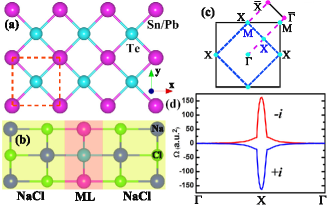
Bulk SnTe and PbTe share the same face-centered cubic NaCl-type structure with an inverted band structure at the point, which results in the realisation of a 3D TCI state in bulk SnTe and a 2D TCI state in SnTe multilayers Liu . On the other hand, PbTe both in bulk and in thin (001) films is in the normal insulator (NI) state Hsieh ; Liu . Here, we focus on the (001) oriented monolayers of SnTe and PbTe. In Fig. 1(a) the top view of such 2D monolayer is shown, with Sn (Pb) and Te atoms forming two square sublattices positioned in the mirror plane . Accordingly, all Bloch states in the system can be labeled with the eigenvalues of the reflection operator with respect to this symmetry plane.
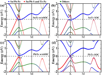
To get a preliminary insight into the topological properties of the systems, we present in Fig. 2 the orbitally-resolved band structures of SnTe and PbTe monolayers with and without SOC. In the absence of SOC for SnTe, energy bands with the Sn- and Te- orbital character (positive parity with the inversion center at the Sn atom) overlap around the -point with the Sn- states (negative parity). For PbTe at the -point without SOC a direct band gap appears with the valence band maximum (VBM) and the conduction band minimum (CBM) dominated by the Pb- and Te- orbitals (positive parity), and the Pb- orbital (negative parity), respectively. Turning on SOC leads to insulating character in both systems (calculated band gaps are 0.05 eV for SnTe and 0.09 eV for PbTe), and to the band inversion in PbTe, so that with SOC the band structure is inverted in both systems.
Owing to an even number of points in the Brillouin zone (see Fig. 1(c)) neither the SnTe monolayer nor the PbTe monolayer is a 2D TI. However, taking the mirror symmetry into account, similarly to bulk SnTe Hsieh , for both SnTe and PbTe monolayers band inversion results in the realisation of a 2D TCI state. To show this explicitly, we calculate the so-called mirror Chern number , where and are Chern numbers of all occupied bands with opposite mirror eigenvalues and , respectively Teo . The Chern number of a given subset of states is given by , where is the Berry curvature Thouless ; yao :
| (1) |
with as band indices which run over considered subset of states, and are corresponding Bloch states and their eigenenergies, and as the cartesian components of the velocity operator. In Fig. 1(d), we plot the distribution of the Berry curvature of all occupied bands with mirror eigenvalue . The main contribution to the Berry curvature comes from the region around , with its values having opposite sign for opposite eigenvalues. The Chern number for each polarization is, respectively, and , yielding the total Chern number of all occupied states and the mirror Chern number . The calculated mirror Chern number proves the TCI nature of (001) oriented SnTe and PbTe monolayers. 111The fact that in Ref. Liu only films thicker than four layers were found to be TCIs might be traced back to the fact that the film bandstructures were modeled from bulk DFT results in that work. Here, DFT calculations were performed explicitly for the films.
One of the prominent features of a TCI is the existence of gapless edge states that appear as a result of the crystal mirror symmetry only and do not require TRS Fu ; Hsieh . To illustrate this, using description in terms of MLWFs of 2D monolayers, we construct the tight-binding Hamiltonian of finite 80-atom wide ribbons oriented along the (110)-axis. In addition, by computing the matrix elements of the Pauli matrices in the basis of MLWFs, we consider the effect of an exchange field applied to our ribbon, which breaks the TRS and generally has out of plane ( term in the Hamiltonian) and in-plane ( term) components. By introducing such an exchange field we aim at mimicking the effect of interaction with a magnetic environment, e.g. magnetic adatoms or magnetic substrate Inoue .
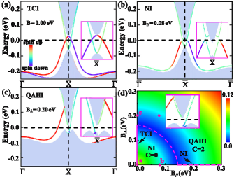
The spin-resolved band dispersion of states localized at the “upper” (“lower”) edge and the projected bulk band structure without any exchange field is presented in (the inset of) Fig. 3(a). Clearly, according to the mirror Chern number analysis, two pairs of edge states cross slightly away from the time-reversal invariant -point, and the spin polarization of the crossing states is of the same sign, which is in contrast to the case of 2D TIs. For an in-plane exchange field the mirror symmetry is broken and the edge states become gapped (Fig. 3 (b)). If the exchange field is, on the other hand, out of plane, the mirror symmetry survives and the system continues to exhibit gapless edge states, although the TRS is broken.
The TRS breaking causes an exchange splitting between conduction and valence bands of opposite spin, and thus, with increasing strength of the exchange field they approach each other. As shown in Fig. 3(d), with increasing the magnitude of the band gap decreases with the system remaining a TCI, and it closes at around eV, reopening again with further increasing . According to our calculations, this signals a phase transition from a 2D TCI to a QAH phase, of which the latter is characterized by a non-zero Chern number of . The nonzero Chern number is further verified by the presence of two gapless edge states on each side of the ribbon within the nontrivial band gap (see Fig. 3(c)).
Our most interesting finding is that the QAH state in our TCI system can be reached irrespective of whether the mirror symmetry is broken by or not (see computed phase diagram in Fig. 3(d) and the inset of it). This means that TCIs can be used to arrive at novel Chern insulators despite their apparent fragility to the mirror symmetry breaking, e.g., by a substrate. In fact, it is only the magnitude of the exchange field and not its direction, which the evolution of the topological band gap is sensitive to, except for the situation with , when the system always resides in the NI state. Such a peculiar behavior also means that, when the QAH state is achieved in the system, it is not only robust with respect to the crystal symmetry, but also to the direction magnetization of adatoms or the substrate, which is subject to thermal fluctuations.
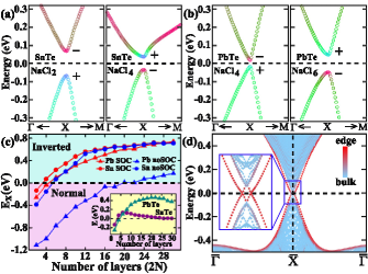
Finally, we choose the widely used material NaCl Zemel to propose a practical way of stabilizing the 2D TCIs while keeping the mirror symmetry in NaCl2N(Sn/Pb)Te1 quantum wells. One of our main findings here is that the magnitude of the TCI band gap can be engineered by the thickness of NaCl spacer, and it can reach as much as 0.13 eV and 0.47 eV in NaCl2NSnTe1 and NaCl2NPbTe1 wells, respectively. The sketch of the crystal structure of a NaCl2N(Sn/Pb)Te1 quantum well is shown in Fig. 1 (b). A SnTe (PbTe) monolayer is placed in between -layers thick NaCl films, so that the mirror symmetry survives. When SnTe (PbTe) monolayer is sandwiched between NaCl slabs, the interaction between SnTe (PbTe) and NaCl pushes the Sn/Pb- orbital up in energy and Sn/Pb- with Te- orbitals down in energy at the point. For the case of the strongest interaction is observed, resulting in the disappearance of the band inversion and the TCI phase. With increasing thickness of NaCl layers, the strength of the local potential decreases. Consequently, the band inversion and the TCI phase return at a critical NaCl thickness.
To show the thickness-dependent band inversion, we plot the orbitally-resolved band structures in Fig. 4(a,b). We observe that for small the Sn/Pb- and Te- orbitals contribute to the VBM with positive parity, while, at larger NaCl thickness, they contribute to the CBM keeping positive parity. Therefore, the band inversion occurs at and for the NaCl2NSnTe1 and NaCl2NPbTe1, respectively. Fig. 4(c) shows the magnitude of the energy gaps at the point without and with SOC versus the NaCl thickness. For NaCl2NSnTe1, the existence of the normal energy gap in both cases demonstrates a normal insulator phase for . For , a SOC-induced band inversion appears, indicating the realisation of the 2D TCI phase. As the NaCl thickness increases further, the energy gap at the point increases and the inverted energy gap is obtained even without SOC. Similar behaviour is seen for NaCl2NPbTe1 with varying , but the influence of SOC is more pronounced in this case. The 2D TCI state is further explicitly confirmed by the topological analysis and the emergence of the gapless edge states in 1D nanoribbons (see Fig. 4(d)). The global energy gap is one of the defining properties of TCI. As shown in the inset of Fig. 4(c), the global gap survives for a large range of NaCl thickness, and its magnitude can be tuned by a proper choice of , reaching as much as 0.13 eV and 0.47 eV for NaCl6SnTe1 and NaCl22PbTe1, respectively. We note that the latter value of 0.47 eV is the largest for either 2D or 3D TCIs reported so far.
In summary, we have identified by first-principles calculations that the (001) oriented SnTe and PbTe monolayers are topological crystalline insulators. We explore the phase diagram of these materials with respect to an applied exchange field due to magnetic adatoms/substrate. We show that as the mirror symmetry remains for the out of plane magnetization, the gapless edge states survive, but the TCI state is destroyed for an in-plane exchange field. For finite , upon reaching a certain strength of the exchange field we show the emergence of a robust Chern insulator phase which survives irrespective of the mirror symmetry breaking. We further show that the large-gap TCI Pb/SnTe based family can be successfully stabilised in NaCl2N(Sn/Pb)Te1 quantum wells. Especially for NaCl22PbTe1, an energy gap of 0.47 eV appears, which is by far larger than that in known 2D and 3D TCIs.
Acknowledgements.
We are grateful to Hongbin Zhang for insightful discussions. This work was supported by the SPP 1666 of the German Research foundation (DFG) and the HGF-YIG Programme VH-NG-513. We acknowledge computing time on the supercomputers JUQUEEN and JUROPA at Jülich Supercomputing Centre and JARA-HPC of RWTH Aachen University.References
- (1) L. Fu, Phys. Rev. Lett. 106, 106802 (2011).
- (2) T. H. Hsieh, H. Lin, J. Liu, W. Duan, A. Bansil, and L. Fu, Nat. Commun. 3, 982 (2012).
- (3) M. Z. Hasan and C. L. Kane, Rev. Mod. Phys 82, 3045 (2010).
- (4) X. L. Qi and S. C. Zhang, Rev. Mod. Phys. 83, 1057 (2011).
- (5) Y. Tanaka, Z. Ren, T. Sato, K. Nakayama, S. Souma, T. Takahashi, K. Segawa, and Y. Ando, Nat. Phys. 8, 800 (2012).
- (6) P. Dziawa, B. J. Kowalski, K. Dybko, R. Buczko, A. Szczerbakow, M. Szot, E. usakowska, T. Balasubramanian, B. M. Wojek, M. H. Berntsen, O. Tjernberg, and T. Story, Nat. Mater. 11, 1023 (2012).
- (7) S.-Y. Xu, C. Liu, N. Alidoust, M. Neupane, D. Qian, I. Belopolski, J. D. Denlinger, Y. J. Wang, H. Lin, L. A. Wray, G. Landolt, B. Slomski, J. H. Dil, A. Marcinkova, E. Morosan, Q. Gibson, R. Sankar, F. C. Chou, R. J. Cava, A. Bansil, and M. Z. Hasan, Nat. Commun. 3, 1192 (2012).
- (8) C. Yan, J. Liu, Y. Zang, J. Wang, Z. Wang, P. Wang, Z.-D. Zhang, L. Wang, X. Ma, S. Ji, K. He, L. Fu, W. Duan, Q.-K. Xue, and X. Chen, Phys. Rev. Lett. 112, 186801 (2014).
- (9) M. Kargarian and G. A. Fiete, Phys. Rev. Lett. 110, 156403 (2013).
- (10) T. H. Hsieh, J. Liu, and L. Fu, Phys. Rev. B 90, 081112(R) (2014).
- (11) T. Rauch, M. Flieger, J. Henk, I. Mertig, and A. Ernst, Phys. Rev. Lett. 112, 016802 (2014).
- (12) H. Weng, J. Zhao, Z. Wang, Z. Fang, and X. Dai, Phys. Rev. Lett. 112, 016403 (2014).
- (13) M. Ye, J. W. Allen, and K. Sun, arXiv:1307.7191.
- (14) J. Liu, T. H. Hsieh, P. Wei, W. Duan, J. Moodera, and L. Fu, Nat. Mater. 13, 178 (2014).
- (15) E. O. Wrasse and T. M. Schmidt, Nano. Lett. 14, 5717 (2014).
- (16) M. Kindermann, arXiv:1309.1667.
- (17) Y. Okada, M. Serbyn, H. Lin, D. Walkup, W. Zhou, C. Dhital, M. Neupane, S. Xu, Y. J. Wang, R. Sankar, F. Chou, A. Bansil, M. Z. Hasan, S. D. Wilson, L. Fu, and V. Madhavan, Science 341, 1496 (2013).
- (18) M. König, S. Wiedmann, C. Brüne, A. Roth, H. Buhmann, L. Molenkamp, X.-L. Qi, and S.-C. Zhang, Science 318, 766 (2007).
- (19) I. Knez, R. R. Du, G. Sullivan, Phys. Rev. Lett. 107, 136603 (2011).
- (20) E. Tang and L. Fu, Nat. Phys. 10, 964 (2014).
- (21) C. Fang, M. J. Gilbert, and B. A. Bernevig, Phys. Rev. Lett. 112, 046801 (2014).
- (22) F. Zhang, X. Li, J. Feng, C. Kane, and E. Mele, arXiv:1309.7682 (2013).
- (23) F. D. M. Haldane, Phys. Rev. Lett. 61, 2015 (1988).
- (24) R. Yu, W. Zhang, H. Zhang, S. Zhang, X. Dai, and Z. Fang, Science 329, 61 (2010).
- (25) C. Z. Chang, J. Zhang, X. Feng, J. Shen, Z. Zhang, M. Guo, K. Li, Y. Ou, P. Wei, and L. L. Wang, Science 340, 167 (2013).
- (26) C. Niu, G. Bihlmayer, H. Zhang, D. Wortmann, S. Blügel, and Y. Mokrousov, Phys. Rev. B 91, 041303(R) (2015).
- (27) H. Zhang, F. Freimuth, G. Bihlmayer, S. Blügel, and Y. Mokrousov, Phys. Rev. B 86, 035104 (2012).
- (28) J. Wang, B. Lian, H. Zhang, Y. Xu, and S.-C. Zhang, Phys. Rev. Lett. 111, 136801 (2013).
- (29) S. A. Skirlo, L. Lu, and Marin Soljačić, Phys. Rev. Lett. 113, 113904 (2014).
- (30) J. N. Zemel, J. D. Jensen, and R. B. Schoolar, Phys. Rev. 140, A330 (1965).
- (31) www.flapw.de.
- (32) G. Kresse and J. Furthmüller, Phys. Rev. B 54, 11169 (1996).
- (33) J. P. Perdew, K. Burke, and M. Ernzerhof, Phys. Rev. Lett. 77, 3865, (1996).
- (34) A. A. Mostofi, J. R. Yates, Y.-S. Lee, I. Souza, D. Vanderbilt, and N. Marzari, Comput. Phys. Commun. 178, 685 (2008).
- (35) F. Freimuth, Y. Mokrousov, D.Wortmann, S. Heinze, and S. Blügel, Phys.Rev.B 78, 035120 (2008).
- (36) J. C. Y. Teo, L. Fu, and C. L. Kane, Phys. Rev. B 78, 045426 (2008).
- (37) D. J. Thouless, M. Kohmoto, M. P. Nightingale, and M. den Nijs, Phys. Rev. Lett. 49, 405 (1982).
- (38) Y. Yao, L. Kleinman, A. H. MacDonald, J. Sinova, T. Jungwirth, D. S. Wang, E. Wang, and Q. Niu, Phys. Rev. Lett. 92, 037204 (2004).
- (39) M. Inoue, K. Isgii, and H. Yagi, J. Phys. Soc. Japan, 43, 903 (1977).