Disaggregated and optically interconnected memory: when will it be cost effective?
Abstract
The “Disaggregated Server” concept has been proposed for datacenters where the same type server resources are aggregated in their respective pools, for example a compute pool, memory pool, network pool, and a storage pool. Each server is constructed dynamically by allocating the right amount of resources from these pools according to the workload’s requirements. Modularity, higher packaging and cooling efficiencies, and higher resource utilization are among the suggested benefits. With the emergence of very large datacenters, “clouds” containing tens of thousands of servers, datacenter efficiency has become an important topic. Few computer chip and systems vendors are working on and making frequent announcements on silicon photonics and disaggregated memory systems.
In this paper we study the trade-off between cost and performance of building a disaggregated memory system where DRAM modules in the datacenter are pooled, for example in memory-only chassis and racks. The compute pool and the memory pool are interconnected by an optical interconnect to overcome the distance and bandwidth issues of electrical fabrics. We construct a simple cost model that includes the cost of latency, cost of bandwidth and the savings expected from a disaggregated memory system. We then identify the level at which a disaggregated memory system becomes cost competitive with a traditional direct attached memory system.
Our analysis shows that a rack-scale disaggregated memory system will have a non-trivial performance penalty, and at the datacenter scale the penalty is impractically high, and the optical interconnect costs are at least a factor of 10 more expensive than where they should be when compared to the traditional direct attached memory systems.
1 Introduction
Traditional servers suffer from a resource fragmentation problem where one or more of the resources –compute, memory, network, or storage– become underutilized because of mismatching workload requirements. For example, compute cycles may be fully exhausted before memory capacity is reached, therefore leaving a fraction of the memory unused. Therefore, the “disaggregation” concept has been proposed where the traditional server’s resources are disaggregated, and then placed in shared resource pools [16, 17]. Servers are constructed dynamically on-demand by allocating from these resource pools according to the workload’s requirements. Data gathered from datacenters show that server memory is unused as much as 50% [18, 23, 24, 30]. Therefore, it appears at first that disaggregating processors and DRAM and placing them in their respective pools will be beneficial. However, we note that a modern microprocessor and DRAM have a very strong affinity, and in fact they cannot get close enough as evidenced by the layers of on-chip caches introduced over the years, L1 thru L3 and now an L4 on some processors [8]. Another issue with memory disaggregation is the signal integrity of long links required. Optical interconnects have been proposed as a memory interconnect [1, 2, 27, 4, 14, 19, 15, 13] as they can provide higher bandwidth over longer distances (e.g., tens of meters) than electrical interconnects typically with lower power. Since switching rates and bandwidths of existing memory channels are couple orders of magnitude higher than the existing electrical fabrics optical interconnects may be necessary to access remote memory.
In this paper we evaluate the claimed benefits of memory disaggregation. We construct a simple cost model that includes the cost of increased latency, cost of bandwidth and the datacenter scale savings expected from a disaggregated memory system. We then identify at which levels a disaggregated memory system is cost competitive with a conventional direct attached memory system. The method can be used to evaluate any future memory technology that impacts memory cost, latency, or bandwidth.
2 Disaggregated Memory System
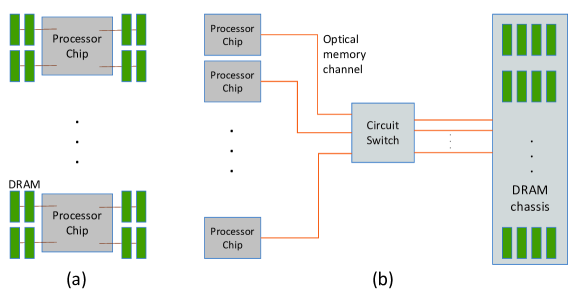
The conventional direct attached memory organization and a disaggregated memory organization are shown in Fig. 1 (a) and (b). In the conventional memory system, a set of DRAM chips on a circuit board called dual-inline-memory module (DIMM) typically plugs into to a server motherboard and connect to the microprocessor typically thru three to four memory channels implementing DDR3 or DDR4 bus protocols.
On the other hand, the disaggregated memory concept that we evaluate in this paper has all the DIMMs in a memory pool as shown in Fig. 1(b). The memory pool could be a memory chassis within a server rack, or memory-only racks that serve a row of racks, a PoD, or the entire datacenter. As such the DIMMs are relatively distant from the processors.
Modern per processor socket memory bandwidths range in the order of 50 to 200 GB/s, about 1 to 2 orders of magnitude higher than state of the art network bandwidths. The processor memory bandwidth depends on the number of memory channels, typically 3-4, and the DRAM frequency. To overcome the distance problem in a disaggregated memory system at such high data rates optical interconnects may be necessary in this concept. Optical links may carry the DDR3, DDR4 or yet to be invented future memory channel protocols. The optical network may span the entire datacenter or may stay within a rack in a more modest implementation. Processors must implement optical transceivers near by to avoid power and wiring density issues. Likewise, memory devices and/or controllers in the pooled memory must also interface to optical transceivers.
The memory pool must be connected to the processors through a switch and memory controllers. Traditional packet switched networks are likely to add a prohibitive amount of latency to the memory access time. One other option is an Optical Circuit Switch (OCS) interconnecting all of the pooled processors and pooled memory to achieve a constant memory latency [4](an upcoming workshop of interest [20]). An OCS, for example the 320 port switch from Calient systems [3] contains a micro-electro-mechanical system (MEMS) of electrically aligned mirrors that direct light beams from inputs to outputs. This MEMS based implementation of OCS has a relatively long circuit setup latency (of the order 50 milliseconds), however in the disaggregated memory application it does not matter; the optical circuit will be set up only once per server configuration. The pass-through latency through the switch is negligible as the path from an input port to an output is merely a couple of mirrors. With a circuit switch (optical or electrical) a dedicated path is set up between two end points: we’re assuming in our analysis that no queueing or processing delays within the switch occurs.
Using an OCS introduces insertion loss (0.8 to 3.5 dB in the case of Calient 320x320). Insertion losses may increase bit error rate of the optical channel and impact performance of the optical transceivers. It should also be noted that MEMS based optical switches today require single mode optical transceivers. This is a market in which prices are coming down relatively quickly due to the maturation of the silicon photonics technology from more expensive Telco market transceivers to the relatively low cost data and computer communication transceivers (which have historically been served by multimode optics).
Note that our cost model neither requires an OCS nor a circuit switch. A packet switch may also be used at the expense of additional hardware cost and potential queuing delays in the switch. The state of the art memory channel protocols, e.g. DDR3 and DDR4, have strict timing requirements and can tolerate neither the distance nor any timing variations in the fabric. Therefore, we’re assuming that a new memory-channel protocol will be specified by the designers of the disaggregated memory systems. Additional memory hierarchies may be necessary such as L4 or L5 caches. We discuss caching after developing the cost model.
Depending on the workload requirements, some number of memory modules are allocated and circuits are set up between the processor chip and the modules. We do not envision multiple processor chips splitting the capacity of a memory module although the cost model does not forbid it.
Note also that the disaggregated memory concept in Fig. 1 (b) is not a shared memory system; each memory module is exclusively accessed by a single processor chip and the memory fabric is not used for interprocessor communication. Any data sharing and coherency protocols are run across a separate fabric such as QPI, not shown.
3 The Cost Model
The disaggregated memory may introduce orders of magnitude higher networking bandwidth and additional memory latencies not present in a direct attached memory system. In this section, we construct a simple cost model shown in Eq. 1 that quantifies the cost of latency, cost of bandwidth, and savings to be achieved from pooling of memory resources. is the net gain expected from disaggregated memory, is memory savings due to pooling of DRAM resources, is the cost of (increased) latency and is the cost of bandwidth:
| (1) |
Note that is the delta cost of optical interconnect (intra or inter rack) over the on-card electrical link cost of a direct attached memory which we assumed to be at most $0.1/Gbps; it includes sockets, connectors, and a circuit board (and the cost may be even less in low end systems).
Note also that Eq. 1 is equally applicable to a “partially disaggregated memory” where some amount of processor local memory serves as a cache of the remote disaggregated memory. Caching reduces the average memory latency which will result in a smaller cost as we will show in the following sections.
3.1 Cost of latency: performance vs. latency
In this section we develop two equations: processor performance as a function of memory latency and processor price as a function of performance. By combining the two, we obtain the cost of increased latency due to memory disaggregation.
DRAM latency is an important element of processor performance. Note that we are referring to the latency of reading one cache line, typically 64 to 128 bytes from memory to the processor cache, which is typically in the range of 50 to 100 nanoseconds. We’re not referring to the message passing latency over Ethernet or Infiniband fabrics found in distributed computing systems. Distributed computing applications explicitly send and receive messages and therefore they can amortize and hide the cost messaging latencies by using large packet sizes and asynchronous messages, which is not practical at the processor instruction level. If applications are to explicitly access the remote memory, using RDMA for example, then that scenario would most likely call for a distributed memory cluster, not the load/store memory architecture shown in Fig. 1(b).
We quantified processor performance as a function of memory latency using a cycle accurate processor simulator. We simulated instruction traces of several benchmarks using different memory latencies and derived a linear relationship between performance and latency. Memory latencies ranged from 75 ns to 300 ns. Two hypothetical processors P1 and P2 were simulated. P1 is a 12 core microprocessor with 64KB L1, 512KB L2, and 8MB L3 caches per core. P2 is the 16 core version of P1. Both P1 and P2 use out-of-order execution. P1 can issue 10 instructions per cycle to 16 functional units in each core. Each core can have up to 16 outstanding cache misses.
Both processors implement simultaneous multithreading / hyperthreading found in x86 and PPC processors [12, 25]. In the SMT mode each core supports 2, 4 or 8 logical processors that share core’s functional units and the execution pipeline, therefore increasing the total core throughput by a factor of 2 to 3.
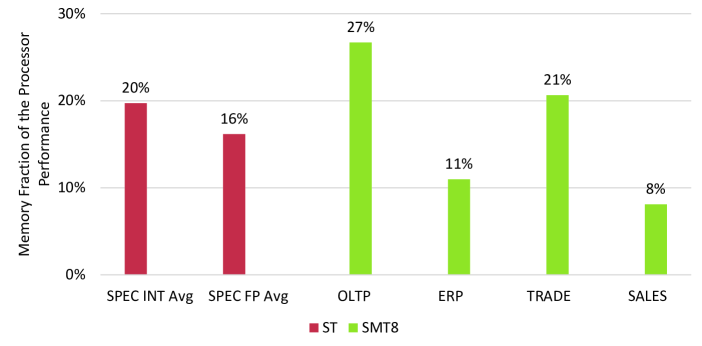
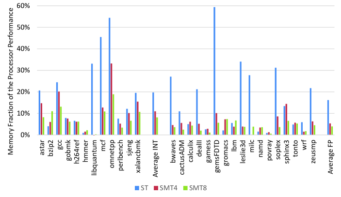
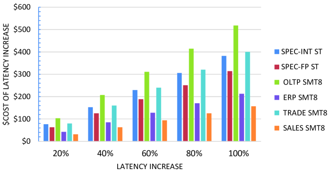
The SPEC CPU2006 Integer and Floating Point suite of benchmark [26] traces were simulated on P2. The reader might critique using the SPEC suite here as it is not a “cloud” benchmark and it is old etc. However it is the leading benchmark for evaluating processor performance which is our focus. For example, 15 papers out of 42 used the SPEC suite at the ISCA’2014 symposium. Four commercial benchmarks OLTP, ERP, TRADE, and SALES were simulated on P1. OLTP is an online transaction processing benchmark that measures the rate of queries/transactions performed on a database. TRADE is a Java based stock trading application. ERP is an enterprise resource planning application. SALES is a customer order processing and distribution application.
We quantified workload’s sensitivity to memory latency as the Memory Fraction of Performance () in Eq. 2
| (2) |
where is the percent increase in benchmark execution time divided by the percent increase in the memory latency, , each relative to its baseline value.
In essence, MFP is the fraction of execution time attributable to the memory latency. For example, MFP=40% indicates that the memory latency is responsible for 40% of the execution time. Suppose the memory latency doubled from a base of 75ns to 150ns. Execution time would increase by 40%. A workload with a small MFP, e.g. MFP=0% is insensitive to the memory latency, because most likely its working set fits in to the processor’s on-chip caches.
Fig. 2 summarizes the memory latency sensitivity for commercial and SPEC benchmarks. Fig. 3 shows the memory latency sensitivity of the SPEC 2006 suite of benchmarks in detail. Average MFP for the INT and FP suites are 20% and 16% on single threaded (ST) cores. Individual benchmarks have an MFP as high as 59%, which shows the problem that disaggregated memory designers will face. For a processor and memory few racks apart (with a round trip delay of 20m x 5ns/m = 100ns), the total memory latency will be more than double the base latency.
A noteworthy observation is that with the increasing SMT levels MFP decreases for most of the benchmarks. SPEC INT average MFP=20% on the ST core reduces to MFP=8% on the 8 threaded SMT8 core. In other words, workloads are more tolerant to increasing memory latencies on an SMT processor, consistent with our expectations. Threads of a core must wait for each other while accessing the shared functional units and pipeline stages, which hides some portion of the memory latency. Results suggest that disaggregated memory systems and other high latency memory systems may benefit from even higher SMT parallelism.
In a disaggregated memory system, the memory latency may increase because of distance, queueing/buffering delays if any, electrical/optical conversion, and protocol delays. Distance will add about 1 ns to the latency per 0.2 meter. A memory chassis in a single rack will add about 6 meters roundtrip (30 nanoseconds or 40%) to the base latency of 75ns. Memory racks serving an entire data center will add possibly 100 meters–roundtrip (500ns), or more to the latency. Another small source of delay is the serialization and deserialization (SerDes) function required in a serial optical communication link. This can be about 10ns, especially if the gear box is a large or an odd ratio (e.g. 25/10) [10]. Forward Error Correction (FEC) or scrambling is often applied to the serialized data packets, also adding latency depending on the FEC code length chosen. While these latencies can be negligible today (e.g. 64/66 Ethernet scrambling or 8b10b block coding), the reduced noise margins at higher data rates is driving potential use of more complex FECs, e.g. adding 100ns latency for 4-6dB of link margin [29], with similar latencies in electrical backplanes (IEEE 802.3bj clause 91) and adoption into emerging single mode optics formats [21, 6].
Some of these variables and design choices are unknown at this time. Therefore to cover a range of design choices in this paper we used latency increases from 0% to 100% over the base latency of 75ns up to a max of 150ns. This range covers a rack scale memory disaggregation and maybe side by side rack dissagregation. Processor performance quickly drops with farther distances therefore we limit our analysis to the 70 – 150ns range.
3.2 Cost of latency: price vs performance
In this section, we quantify the cost of the disaggregated memory latency. Suppose the direct attached memory is to be replaced with a disaggregated memory system. How would one quantify the monetary value of the latency increase? We reasoned that the datacenter operator would want to compensate or at least know the cost of any compute cycles lost to the increased latency. One approach for compensation may be deploying more servers in the datacenter. A cheaper approach may be upgrading to a higher performance processor along with the disaggregated memory, therefore having the same datacenter performance before and after.
In our model, we use the higher performance processor’s price delta as a proxy for the cost of increased memory latency. (Note that we’re not advocating using faster processors with disaggregated memory systems. We’re merely quantifying the cost of latency via processor price.) For a given memory latency increase, we choose a higher throughput processor in the following manner:
| (3) |
which will have an equal performance with the old processor using a direct attached memory system (where is the workload’s memory fraction of execution time as stated before.)
Note that we’re not concerned with the internal organization of this higher throughput processor. The performance increase can come from higher MHz, bigger or additional caches, or more cores. We need only the delta cost of the processor for the cost analysis. Also note that our method of using processor price as a proxy is general enough that it may be used to quantify the performance cost of any new memory technology or memory fabric.
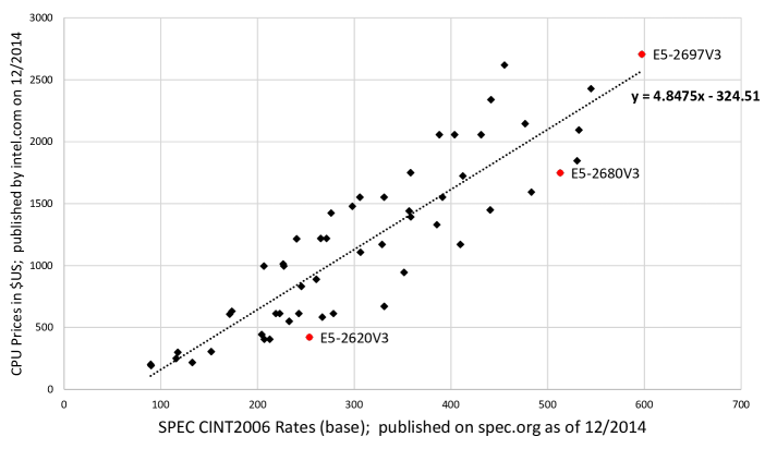
Next, we derive the price and performance relationship: we retrieved 2240 official benchmark reports from www.spec.org submitted by computer system vendors for a total of 54 models of Intel E5-2xxx v2 and v3 series processors. The SPEC CPU2006 “base rate” metric measures the throughput of a processor. The lowest throughput processor in the list, E5-2403v2, has 4 cores, 1.8GHz clock, 10MB cache and has a SPEC integer (INT) rate of 90. The highest throughput E5-2697v3, has 14 cores, 2.6GHz clock, 35MB cache and has an INT rate of 597 (faster E5 processors were on spec.org, however their prices were not available on intel.com). Different vendors reported slightly different rate values for the same model processor, may be due to the differences in their benchmark configuration or software. We averaged them to arrive at a single rate for the same model processor.
We then retrieved the prices of E5 v2 and v3 processors from intel.com (retrieved on Dec. 2014), and plotted the cost vs. performance data point of each processor model on Fig. 4. We then fitted those data points with a least squares fit trend-line describing the relationship between cost and performance
| (4) |
Note that the function is not a perfect fit because price is not necessarily determined only by the performance. Processors have other differentiating characteristics, for example some are low-voltage low-power parts, some have different QPI bandwidths, some may have been manufactured with a different process. Intel sets the prices however it chooses. But, a strong dependence between price and performance is apparent in Fig. 4.
For the sample calculations, we assumed that the conventional direct attached memory system’s processor has a SPEC INT rate of 400. If for example memory disaggregation increases execution time by 10%, then one could compensate for that loss by choosing a processor with a rate of 440, and the cost of that +40 rate increase can be estimated from the fitted line in Fig. 4.
3.3 Cost of bandwidth
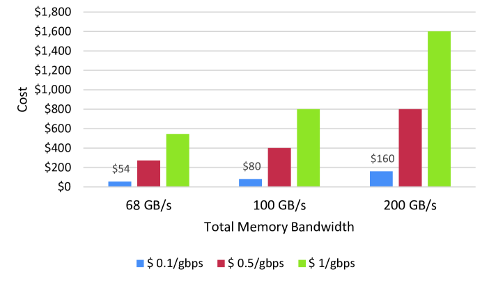
Memory bandwidth requirements of state of the art microprocessors are a couple orders of magnitude higher than the data communication network bandwidths. For example the faster models of Intel E5-2xxx processors on the right hand side of Fig. 4 all have a total memory bandwidth of 68 GB/s (GB: gigabytes). The E7 models, not shown here, have 85 GB/s memory bandwidth. The IBM Power8 processors have in excess of 230 GB/s of bandwidth [8]. Therefore, we expect memory disaggregation to highly burden the networking costs. Fig. 6 shows the cost of bandwidth for different unit costs. Some historical examples of B/W cost trends for different optical interconnect form factors [28] show costs at several dollars per Gbps in 2012 heading towards $1/Gbps in 2015. It should be noted that these are form factor/standard dependent transceiver costs and that cabling and connector costs can add 25% or more (distance dependent). Furthermore, these transceivers are for multimode fiber and not suitable for use with OCS MEMS switches (another component which if used adds additional cost). The costs for single mode optical interconnects, however, are declining rapidly with the maturation of Si Photonics technology, and while more difficult to predict, could optimistically be assumed to be on par with multimode transceivers in the not too distant future.
As stated before, there are many designs choices to be made. Instead of predicting the future cost of silicon photonics, we simplify the problem by calculating the unit bandwidth cost required to make the disaggregated memory system and the direct attached memory system have an equal-performance and equal-cost. We set the left hand side of Eq. 1 to zero () and rearrange the terms as
| (5) |
We can calculate the right hand side of the equation, therefore arriving at a bandwidth cost that has parity with a direct attached memory system. As stated before in our calculations we assumed a unit cost of $0.1/Gbps for the direct attached memory interconnect.
3.4 Disaggregated Memory Savings
The promise of disaggregated memory is the efficiencies to be achieved from pooling the memory resources. Through pooling, unused memory fragments otherwise locked in individual servers will be made available to the entire datacenter. Few data points on unused memory capacities exist in the literature. Samih reports that only 69% of the memory capacity is used in a cluster of 437 TB size cluster [24]. Meng reports 45% reduction in data center resource requirements when virtual machines with complementary resource requirements are provisioned jointly [18]. Reiss reports that memory usage does not exceed about 50% of the capacity of a Google cluster [23]. Qi reports memory usage of five Google backend clusters each of which consisting of thousands of machines. The five cluster’s memory utilitizations are approximately 50, 10, 30, 55, and 65% respectively [30].
Using these existing data points, we assume in our example calculations that memory disaggregation will save as much as 50% of the memory capacity. We also assume that each processor socket has a maximum 128 GB DRAM attached at a cost of $7.125 per GB (8 DIMMs x 16 GB/DIMM). Higher DRAM densities and capacities call for stacked DIMMs which are very expensive and many cloud providers will not use. For example, Softlayer–a cloud provider advertises a maximum of 128GB RAM per socket in its “bare-metal” servers. In sum, 50% savings of DRAM capacity translates to $456 memory savings per processor socket.
4 Putting things together: equal cost - equal performance
Now that we have quantified both the cost of latency and the savings from disaggregated memory, we can calculate the unit cost of bandwidth in terms of dollars per Gbps.
For a given system configuration, workload and memory latency increase we lookup the memory savings and the cost of latency increase , and then calculate per Eq. 5. Then the unit bandwidth cost for an equal cost equal performance system is
| (6) |
Note that the unit cost must include all the fabric components shown in Fig. 1(b): optical interconnect, the OCS switch (if used), cabling etc.
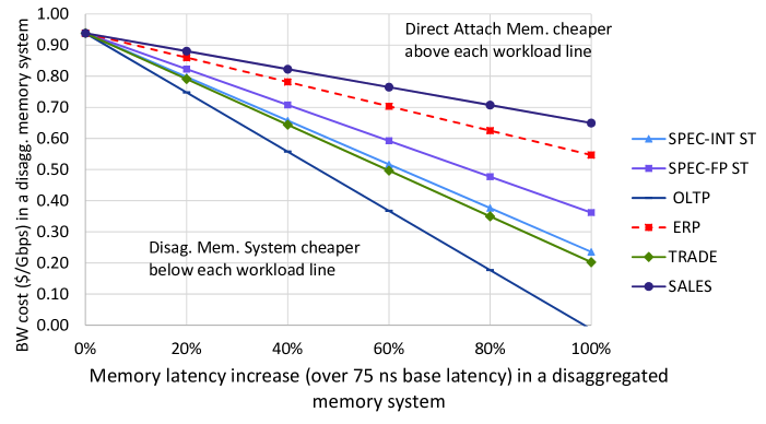
Fig. 7 gives the equal cost equal performance lines for a direct attached memory system and a disaggregated memory system as a function of the latency increase due to disaggregation. For a given workload and a latency increase, if the disaggregation unit cost is below the line, then the disaggregated memory is cheaper because the memory savings outweigh the cost of disaggregation. Otherwise, if the unit cost is above the line, then the direct attached memory solution is cheaper. It’s apparent from the set of lines that for a given unit cost –i.e. a horizontal line across the graph– as the memory latency increases the savings due to disaggregated memory diminish. A rack scale disaggregated memory will add about 30ns roundtrip for distance alone (40%). Including the logic delays a total latency increase of 40% seems optimistic at the rack scale. SPEC integer and OLTP workloads require unit costs to be lower than $0.70/Gbps and $0.55/Gbps in this scenario.
It is also apparent that workload performance with the strongest dependence on memory latency, such as OLTP require unit costs to be cheaper for disaggregated memory. Another observation is that the Y-axis intercept (for a 0% latency increase) $0.94/Gbps, is largely determined by the memory bandwidth requirement of the processor chip (68GB/s in the example.) A processor with higher memory bandwidth will require the disaggregated memory fabric to be even cheaper and the Y axis intercept must be smaller. Alternatively, to make the case for using a disaggregated memory, the higher bandwidth processor needs to attach to more than 128GB of direct attached memory to make the memory savings worthwhile.
5 Conclusions
In this paper we developed a simple model of cost vs. performance for a disaggregated memory system. The model may also be used for verifying cost-performance benefits of future memory technologies and memory fabrics.
We showed the performance dependency on the memory latency, and that any latency increase has a non-trivial cost. We showed that disaggregated memory needs to have a very low latency to be feasible and therefore needs to be implemented at the rack level to minimize the distance. Additional cache layers may be required in the memory hierachy to overcome the latency and bandwidth issues.
Our simulations showed that for many workloads, sensitivity to memory latency decreases with increasing SMT / hyperthread counts. Therefore, hyperthreaded cores may become an important feature in disaggregated systems.
We demonstrated the equal cost and equal performance curves for a disaggregated memory system. Using today’s prices of processor and memory we arrived at a $0.94/Gbps cost for the disaggregated memory fabric with a 0% latency penalty, and approximately $0.5/Gbps cost with a 50% latency penalty. The unit cost must include all the component costs from processor’s memory channel to the switch to the DRAM chassis containing the pooled memory. Actual cost of photonics fabric are in excess of $1/Gbps for transceiver alone today and possibly $1.5/Gbps with cabling. An OCS switch costs around $300/port which adds another $3/Gbps with 100 Gbps links. Therefore, the memory dissagregation concept analyzed in this paper does not appear to be an economical solution. To justify the practical investment in a disaggregated memory application, we would like to see the optical memory interconnect cost to decrease by at least a factor of 3-4 without an OCS and a factor of 9-10 with an OCS. At this time, disaggregation and optical interconnects appear more suitable for I/O, for example PCIexpress which is less sensitive to latency and has lower bandwidth than memory.
Note that recent advances in virtual machines and application “containers” may make our 50% memory savings assumption optimistic, which is another argument against disaggregated memory. Virtualization simplifies bin-packing of workloads in to underutilized servers. Furthermore, live migration of VMs and containers [11, 7] can move workloads across the datacenter transparently and dynamically in response to changing resource requirements, a property that the statically partitioned memory pool in Fig. 1(b) does not have. As stated before, Meng reports that by jointly placing VMs with complementary resources on the same server, datacenter resource requirements can be reduced by 45% [18]. Isci reports an RDMA based live migration technique that can migrate virtual machines near the network line rate of 40 Gbps which will be beneficial if workloads have rapidly changing resource requirements [11]. Therefore, the disaggregated memory systems of the future may be more relevant to the “bare-metal” cloud infrastructures or very large workloads that cannot be colocated with other workloads.
Our study focused on the acquisition costs. We did not consider the total cost of ownership, for example potential energy savings due to the disaggregated memory and silicon photonics over the electrical interconnects.
We did not study the cost-performance of adding another cache layer to the architecture in Fig. 1(b). Han suggests that some amount of local memory can be a cache of the remote memory [9] and assumes a page level (4KB) access to the remote memory by exploiting processor’s address translation hardware. However, we know from our own unpublished work that software based “fast paging” to a remote or slower second tier memory does not work very well for many workloads. Page fault handling has a latency of a few microseconds at minimum depending on the operating system. Han [9] also mentions this as a caveat. Samih [24] shows a slowdown of 1 to 2 orders of magnitude in the Hadoop Sort application when comparing a paged local-to-remote memory system to a system with enough local memory. When a system starts “fast paging” to a slower memory not only the increased latency but the system cycles wasted in the kernel reduce workload performance significantly.
Another issue with page level remote memory access is the network bandwidth explosion. One hopes for some spatial locality, however except for sequential access patterns the 4KB size pages over the fabric often transport large amounts of unused data as the processor’s unit of memory access is only 64 bytes.
An alternative to the software based paging is implementing a hardware cache controller and a directory, and using the local DRAM as the cache of the remote DRAM (e.g. a partially disaggregated memory system), and using a cache block size smaller than a page. These approaches should perform better than software based paging, however they have design challenges and cost to analyze (for example [5, 22]) that we did not cover here and we leave it as future work.
References
- [1] M. Asghari and A. V. Krishnamoorthy. Silicon photonics: Energy-efficient communication. Nature Photonics, 5(5):268–270, 2011.
- [2] C. Batten, A. Joshi, J. Orcutt, A. Khilo, B. Moss, C. W. Holzwarth, M. A. Popovic, H. Li, H. I. Smith, J. L. Hoyt, F. X. Kartner, R. J. Ram, V. Stojanovic, and K. Asanovic. Building Many-Core Processor-to-DRAM Networks with Monolithic CMOS Silicon Photonics. IEEE Micro, 29(4):8–21, 2009.
- [3] Calient. 3D MEMS Optical Circuit Switching for Software Defined Data Centers and Metro Networks http://www.calient.net. accessed: 2015-01-15.
- [4] A. Chakraborty, E. Schenfeld, and M. Silva. Switching Optically-Connected Memories in a Large-Scale System. In Parallel & Distributed Processing Symposium (IPDPS), 2012 IEEE 26th International, pages 727–738. IEEE, 2012.
- [5] C. C. Chou, A. Jaleel, and M. K. Qureshi. Cameo: A two-level memory organization with capacity of main memory and flexibility of hardware-managed cache. In Microarchitecture (MICRO), 2014 47th Annual IEEE/ACM International Symposium on, pages 1–12, Dec 2014.
- [6] CLR4-Alliance. Specification for 100Gb/s Coarse Wavelength Division Multiplex Optical Data Transmission. https://www.clr4-alliance.org/media/doc/100G-CLR4-Specification_v1p353.%pdf, 2014.
- [7] CRIU. Live migration for containers is around the corner; http://criu.org. accessed: 2015-01-15.
- [8] J. Friedrich, H. Le, W. Starke, J. Stuechli, B. Sinharoy, E. J. Fluhr, D. Dreps, V. Zyuban, G. Still, C. Gonzalez, et al. The POWER8 processor: Designed for big data, analytics, and cloud environments. In IC Design & Technology (ICICDT), 2014 IEEE International Conference on, pages 1–4. IEEE, 2014.
- [9] S. Han, N. Egi, A. Panda, S. Ratnasamy, G. Shi, and S. Shenker. Network Support for Resource Disaggregation in Next-generation Datacenters. In Proceedings of the Twelfth ACM Workshop on Hot Topics in Networks, HotNets-XII, pages 10:1–10:7, New York, NY, USA, 2013. ACM.
- [10] INPHI. CMOS PHY/SerDes Gearbox with Tri-Rate Support for 10G, 40G and 100G Ethernet and OTN Line Cards; http://www.inphi.com/media-center/press-room/press-releases-and-media-alerts/inphi-delivers-2nd-generation-cmos-physerdes-gearbox-with-tri-rate-support-for-10g-40g-and-100g-ethernet-and-otn-line-cards.php. accessed: 2015-01-15.
- [11] C. Isci, J. Liu, B. Abali, J. O. Kephart, and J. Kouloheris. Improving server utilization using fast virtual machine migration. IBM Journal of Research and Development, 55(6):4–1, 2011.
- [12] D. Koufaty and D. T. Marr. Hyperthreading technology in the netburst microarchitecture. Micro, IEEE, 23(2):56–65, 2003.
- [13] C.-S. Li, C. M. Olsen, and D. G. Messerschmitt. Analysis of crosstalk penalty in dense optical chip interconnects using single-mode waveguides. Lightwave Technology, Journal of, 9(12):1693–1701, 1991.
- [14] C.-S. Li and H. S. Stone. Differential board/backplane optical interconnects for high-speed digital systems. part 1: Theory. Journal of lightwave technology, 11:1234–1249, 1993.
- [15] C.-S. Li, H. S. Stone, Y. Kwark, and C. M. Olsen. Fully differential optical interconnections for high-speed digital systems. Very Large Scale Integration (VLSI) Systems, IEEE Transactions on, 1(2):151–163, 1993.
- [16] K. Lim, J. Chang, T. Mudge, P. Ranganathan, S. K. Reinhardt, and T. F. Wenisch. Disaggregated memory for expansion and sharing in blade servers. In ACM SIGARCH Computer Architecture News, volume 37, pages 267–278. ACM, 2009.
- [17] K. Lim, Y. Turner, J. R. Santos, A. AuYoung, J. Chang, P. Ranganathan, and T. F. Wenisch. System-level implications of disaggregated memory. In High Performance Computer Architecture (HPCA), 2012 IEEE 18th International Symposium on, pages 1–12. IEEE, 2012.
- [18] X. Meng, C. Isci, J. Kephart, L. Zhang, E. Bouillet, and D. Pendarakis. Efficient resource provisioning in compute clouds via vm multiplexing. In Proceedings of the 7th international conference on Autonomic computing, pages 11–20. ACM, 2010.
- [19] C. M. Olsen and C.-S. Li. Differential board/backplane optical interconnects for high-speed digital systems. ii. simulation results. Lightwave Technology, Journal of, 11(7):1250–1262, 1993.
- [20] OSA. Workshop on Photonics for Disaggregated Data Centers. In OFC’2015, 2015.
- [21] T. Palkert. 100G PSM4 Specification; Parallel Single Mode 4 Lane. http://www.psm4.org/100G-PSM4-Specification-rev-1-0.pdf, 2014.
- [22] M. K. Qureshi and G. H. Loh. Fundamental latency trade-off in architecting dram caches: Outperforming impractical sram-tags with a simple and practical design. In Proceedings of the 2012 45th Annual IEEE/ACM International Symposium on Microarchitecture, MICRO-45, pages 235–246, Washington, DC, USA, 2012. IEEE Computer Society.
- [23] C. Reiss, A. Tumanov, G. R. Ganger, R. H. Katz, and M. A. Kozuch. Heterogeneity and dynamicity of clouds at scale: Google trace analysis. In Proceedings of the Third ACM Symposium on Cloud Computing, page 7. ACM, 2012.
- [24] A. Samih, R. Wang, C. Maciocco, T.-Y. C. Tai, and Y. Solihin. A collaborative memory system for high-performance and cost-effective clustered architectures. In Proceedings of the 1st Workshop on Architectures and Systems for Big Data, pages 4–12. ACM, 2011.
- [25] B. Sinharoy, R. Kalla, W. Starke, H. Le, R. Cargnoni, J. Van Norstrand, B. Ronchetti, J. Stuecheli, J. Leenstra, G. Guthrie, et al. IBM POWER7 multicore server processor. IBM Journal of Research and Development, 55(3):1–1, 2011.
- [26] SPEC. SPEC CPU 2006 benchmarks. http://spec.org. accessed: 2014-12-25.
- [27] M. Tan, P. Rosenberg, J. S. Yeo, M. McLaren, S. Mathai, T. Morris, H. P. Kuo, J. Straznicky, N. P. Jouppi, and S.-Y. Wang. A high-speed optical multi-drop bus for computer interconnections. Applied Physics A, 95(4):945–953, 2009.
- [28] M. A. Taubenblatt. Optics Technology Trends in Data Centers. http://www.ofcconference.org/library/images/ofc/2014/Market%20Watch%20a%nd%20SPS/6-Taubenblatt.pdf, 2014.
- [29] T. Wang, W. Yang, and X. Wang. Technical Feasibility of 400GE Architecture with Stronger FEC; IEEE 802.3 400GbE Study Group. http://www.ieee802.org/3/400GSG/public/13_11/wang_400_01_1113.pdf, 2013.
- [30] Q. Zhang, J. L. Hellerstein, and R. Boutaba. Characterizing task usage shapes in Google compute clusters. In Large Scale Distributed Systems and Middleware Workshop (LADIS.11), 2011.