Enhanced photogalvanic effect in graphene due to Rashba spin-orbit coupling
Abstract
We analyze theoretically optical generation of a spin-polarized charge current (photogalvanic effect) and spin polarization in graphene with Rashba spin-orbit coupling. An external magnetic field is applied in the graphene plane, which plays a crucial role in the mechanism of current generation. We predict a highly efficient resonant-like photogalvanic effect in a narrow frequency range which is determined by the magnetic field. A relatively less efficient photogalvanic effect appears in a broader frequency range, determined by the electron concentration and spin-orbit coupling strength.
pacs:
72.25.Fe, 78.67.Wj, 81.05.ueIntroduction: Two-dimensional electron systems with spin-orbit (SO) coupling are currently of a broad interest due to the coupled charge and spin dynamics, as revealed in a variety of spin related transport phenomena dyakonov2008 ; sinova2014 ; aronov89 ; edelstein90 . Owing to the SO coupling, the spin dynamics can be generated, among others, by a low-frequency electric field rashba2003 as well as optically by interband electronic transitions stevens2003 ; kato04 ; silov04 . Moreover, an external static magnetic field can enable the current generation by light absorption, leading to a photogalvanic effect ganichev2003 .
Many of the spin related phenomena, including also the ones mentioned above, can be observed in two dimensional graphene monolayers and other graphene-like materials like silicene for instance. The huge interest in graphene is related mainly to its natural two-dimensionality, very unusual electronic structure, and high electron mobility which ensures its excellent transport properties GeimNatMater07 ; katsnelson . Even though the intrinsic SO interaction in free-standing graphene is negligibly small, the Rashba spin-orbit coupling can be rather strong for graphene deposited on certain heavy-element substrates dedkov08 ; varykhalov08 ; zarea09 . Since the electronic band structure of graphene is significantly different from that of a simple two-dimensional electron gas (2DEG), and the spin-orbit coupling creates a gap in the electronic spectrum, graphene can reveal qualitatively new effects which can not be observed in 2DEG in conventional semiconductor heterostructures. Additionally, the SO-related phenomena in graphene are also important from the point of view of potential applications in all-graphene based spintronics devices trauzettel07 ; han2014 ; seneor2012 .
In this letter we predict an enhanced photogalvanic effect in graphene. To do this we consider the charge and spin currents generated in graphene by optical pumping in the infrared photon energy region, and show that the optical pumping can be used to generate in graphene not only the spin density inglot14 , but also a spin-polarized net current. An external magnetic field applied in the graphene plane plays an important role in the mechanism of current generation. We show that the efficiency of current generation per absorbed photon can be very high at certain conditions. Apart from this, we also show that one can create spin density without creating electric current, but not vice versa.
Model: We consider low-energy electronic spectrum of graphene in the vicinity of the Dirac points katsnelson . Additionally, we include the Rashba SO coupling kane05 and the Zeeman energy in a weak external in-plane magnetic field . The corresponding Hamiltonian can be then written in the form
| (1) |
where cm/s is the electron velocity in graphene, and are the Pauli matrices defined in the sublattice space, is the maximum Zeeman splitting, while the and signs refer to the and Dirac points, respectively. Furthermore, with being the Landé factor, and with standing for the Rashba coupling constant rashba09 .
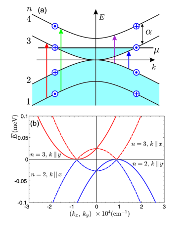
The electronic spectrum corresponding to Hamiltonian (1) consists of four energy bands in each valley, , where to is the band index. The corresponding spectrum for is shown in Fig.1a, and is given by the formula . In turn, the expectation value of the spin in the absence of magnetic field is oriented perpendicularly to the wavevector rashba09 , similarly as in a semiconductor-based 2DEG with Rashba SO coupling. Contrary to the 2DEG, there are, however, no eigenstates of Hamiltonian (1) with a definite eigenvalue of any spin component. This appears due to the specific form of the SO coupling in graphene. The corresponding spin components in the absence of magnetic field and for the wavevector are
| (2a) | |||
| (2b) | |||
where is the absolute value of the electron velocity in the absence of magnetic field. Here the upper and lower signs correspond to the bands (1,4) and (2,3), respectively. Note, both spin components given by Eqs. (2a) and (2b) vanish in the limit of rashba09 corresponding to the mixed rather than pure character of the band states in the spin subspace.
The electronic spectrum presented in Fig.1a is significantly modified by an external in-plane magnetic field. Assume this field is oriented along the axis . The exact electronic spectrum can be then obtained by direct diagonalization of the Hamiltonian (1), and is shown in Fig.1b for wavevectors along the axis and . Only the states corresponding to the bands labeled in Fig.1a with the index 2 and 3 are shown there. As one can note, for one propagation orientation the electron bands are shifted vertically, i.e. to higher (lower) energy, while for the second propagation orientation the bands are shifted horizontally, i.e. to left (right) from the point . The latter separation in the k-space of the bands 2 and 3 is crucial for the enhanced photogalvanic effect. For a weak Zeeman energy, , and for electron momenta of our interest, , the field-dependent correction to the electron energy, calculated by perturbation theory, has the form
| (3) |
where again the upper (lower) sign corresponds to the bands (1,4) and (2,3), respectively.
Assume now that the system is subject to electromagnetic irradiation. Hamiltonian describing interaction of electrons in graphene with the external periodic electromagnetic field, , takes the form
| (4) |
As in Eq. (1), different signs correspond here to electrons within the and valleys.
The injection rate of a quantity , related to the intersubband optical transitions, can be calculated by using the Fermi’s golden rule,
| (5) |
where is the Fermi-Dirac distribution function. Since there are two valleys, and , one needs to calculate contributions to from both of them. The quantities of our interest here are:
| (6) |
for the light absorption (where is the identity operator),
| (7) |
for the corresponding spin component injection, and
| (8) |
for the current injection. Here, , where is the electron charge, while and . The injected spin current, in turn, can be calculated as rioux14
| (9) |
where . Below we concentrate on the results for injection of charge current and spin density.
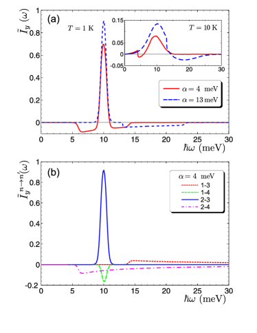
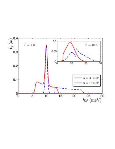
Results: Using equations for the injection rate one can calculate the charge current and spin polarization induced by the optical pumping. Let us begin with the photogalvanic effect, i.e. charge current generation. Results for two different polarizations of the electromagnetic field are presented in Figs. 2 and 3. Here the injection efficiency is defined as , where and is the incident photon flux gusynin06 ; kuzmenko08 ; zulicke10 .
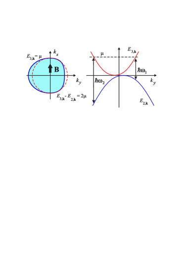
The transitions start at if and at otherwise. In both cases a strong narrow peak in the injection efficiency appears at a resonant energy . This peak is remarkably higher for the electromagnetic field polarized along the static magnetic field , compare Figs. 2 and 3. To understand origin of this peak lat us consider transitions between the subbands marked with and . First, we determine the shape of the isoenergetical line corresponding to a given Fermi energy, . For the band corresponding to , one obtains from Eq. (3) the first-order correction to the Fermi wavevector,
| (10) |
which sets the following boundaries for the Fermi surface:
| (11a) | |||
| (11b) | |||
Due to the -dependent Zeeman term, the Fermi surface becomes considerably deformed and anisotropic, as shown in the left panel of Fig.4. The maximum deformation is independent of the chemical potential and spin-orbit coupling. In turn, the resonance line determined by is still a circle given by the condition
| (12) |
A part of the resonance line is inside the occupied region. Therefore, we have an interval of the photon energies, , as shown in the right panel of Fig.4, where the transitions occur for positive values of , while the transitions with negative (which would compensate partly current) are forbidden. As a result, a very efficient current injection occurs in this photon energy window, as visible in Fig. 2. In the considered regime of , this photon energy interval is determined by the conditions
| (13a) | |||
| (13b) | |||
which results in the peak width given by the formula,
| (14) |
With the increase in temperature to , this effect becomes smeared out by thermal broadening of the Fermi distribution, and the injection rate decreases as shown in the insets to Figs. 2 and 3.
Similar arguments can be also applied to the transitions between and subbands. As a result, one gets a relatively small negative peak in the injection rate at , see Fig. 2 (b). The weakness of this injection channel is due to a relatively small Fermi velocity in the subband 4 at , while its reversed sign is due to the opposite spin orientation in these subbands, which results (similar to Eq. (11a) and Fig. 4) in a different shape of the Fermi surface, where the transitions begin to occur at . In the limit , the positive and negative contributions compensate each other, and the current injection efficiency tends to zero, as expected in the absence of spin-orbit coupling.
Having discussed the strong peaks in the current injection rate, let us consider now briefly the broad structure. It is formed by momentum dependence of the matrix elements and velocity, and has the efficiency of the order of . The current injection stops at , where the contributions due to transitions between different bands compensate each other. We also mention that for , the charge current has only the -component for both polarizations of the incident light.
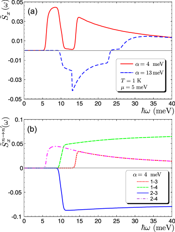
Now let us address briefly the problem of spin and spin current injection. For both incident light polarizations one obtains a net spin polarization along the and axes. The numerical results are presented in Fig. 5 (a) for the total spin polarization , while Fig. 5(b) shows injected spin polarization associated with specific optical transitions. Physical mechanism of the optically injected spin polarization is rather clear, since the spin-flip transitions are related to the above-mentioned fact that the eigenstates of Hamiltonian (1) are not the spin eigenstates, and the broken in magnetic field time-reversal symmetry allows one to inject spin density. Since the charge current is along the -axis, we obtain effectively a spin-polarized current transferring in-plane spin components in the direction. As concerns the spin current defined in Eq. (9), it is symmetric with respect to the time reversal and, therefore, magnetic field produces there only changes proportional to .
Summary: We have calculated optical injection of charge current in graphene as the photogalvanic effect due to spin-orbit coupling norris10 . The current is injected only in a finite range of infrared light frequencies, determined by the chemical potential and the spin-orbit coupling strength. The striking feature of the injection is a narrow peak at the resonant frequency , where the current injection can be very efficient. Comparing the -dependence of the current and spin injection, we conclude that, depending on the light frequency, one can inject either spin-polarized net electric current or net spin polarization without the current injection. This result can be applied to a controllable current generation in spin-orbit coupled graphene.
Acknowledgements. This work is supported by the National Science Center in Poland under Grant No. DEC-2012/06/M/ST3/00042. The work of MI is supported by the project No. POIG.01.04.00-18-101/12. The work of EYS was supported by the University of Basque Country UPV/EHU under program UFI 11/55, Spanish MEC (FIS2012-36673-C03-01), and ”Grupos Consolidados UPV/EHU del Gobierno Vasco” (IT-472-10).
References
- (1) Spin Physics in Semiconductors, (M. I. Dyakonov, Ed.) Springer Series in Solid-State Sciences (Springer, Berlin, 2008).
- (2) J. Sinova, S. O. Valenzuela, J. Wunderlich, C. H. Back, and T. Jungwirth, arXiv:1411.3249.
- (3) A. G. Aronov and Yu. B. Lyanda-Geller, JETP Lett. 50, 431 (1989).
- (4) V. M. Edelstein, Solid State Communications 73 233 (1990).
- (5) E. I. Rashba and Al. L. Efros, Phys. Rev. Lett. 91, 126405 (2003).
- (6) M. J. Stevens, A. L. Smirl, R. D. R. Bhat, A. Najmaie, J. E. Sipe, and H. M. van Driel, Phys. Rev. Lett. 90, 136603 (2003).
- (7) Y. K. Kato, R. C. Myers, A. C. Gossard and D. D. Awschalom, Phys. Rev. Lett. 93, 176601 (2004).
- (8) A. Y. Silov, P. A. Blajnov, J. H. Wolter, R. Hey, K. H. Ploog, and N. S. Averkiev, Appl. Phys. Lett. 85, 5929 (2004).
- (9) S. D. Ganichev, and W. Prettl, J. Phys. Cond. Matter. 15, R935 (2003).
- (10) A. K. Geim and K. S. Novoselov, Nature Mater. 6, 183 (2007).
- (11) M. I. Katsnelson, Graphene: Carbon in Two Dimensions (Cambridge Univ. Press, 2012).
- (12) Y. S. Dedkov, M. Fonin, U. Rüdiger, and C. Laubschat, Phys. Rev. Lett. 100, 107602 (2008).
- (13) A. Varykhalov, J. Sánchez-Barriga, A. M. Shikin, C. Biswas, E. Vescovo, A. Rybkin, D. Marchenko, and O. Rader, Phys. Rev. Lett. 101, 157601 (2008).
- (14) M. Zarea and N. Sandler Phys. Rev. B79, 165442 (2009).
- (15) B. Trauzettel, D. V. Bulaev, D. Loss, and G. Burkard, Nature Phys. 3, 192 (2007).
- (16) W. Han, R. K. Kawakami, M. Gmitra, and J. Fabian, Nature Nanotechnology 9 794 (2014).
- (17) P. Seneor, B. Dlubak, M.-B. Martin, A. Anane, H. Jaffres, and A. Fert, MRS Bulletin 37, 1245 (2012).
- (18) M. Inglot, V. K. Dugaev, E. Y. Sherman, and J. Barnaś, Phys. Rev. B89, 155411 (2014).
- (19) C. L. Kane and E. J. Mele, Phys. Rev. Lett. 95, 226801 (2005).
- (20) E. I. Rashba, Phys. Rev. B79, 161409 (2009).
- (21) J. Rioux and G. Burkard, Phys. Rev. B90, 035210 (2014)
- (22) V. P. Gusynin and S. G. Sharapov, Phys. Rev. B73, 245411 (2006).
- (23) A. B. Kuzmenko, E. van Heumen, F. Carbone, and D. van der Marel, Phys. Rev. Lett. 100, 117401 (2008).
- (24) P. Ingenhoven, J. Z. Bernád, U. Zülicke, and R. Egger, Phys. Rev. B 81, 035421 (2010).
- (25) The proposed mechanism is qualitatively different from the coherent control approach of D. Sun, C. Divin, J. Rioux, J. E. Sipe, C. Berger, W. A. de Heer, P. N. First, and T. B. Norris, Nano Lett. 10 1293 (2010).