Coulomb bound states and resonances due to groups of Ca dimers adsorbed on suspended graphene
Abstract
The electronic bound states and resonances in the vicinity of the Dirac point energy due to the adsorption of calcium dimers on a suspended graphene monolayer are explored theoretically using density functional theory (DFT) and an improved extended Hückel model that includes electrostatic potentials. The Mulliken atomic charges and the electrostatic potentials are obtained from DFT calculations and reveal charge transfer from the Ca dimers to the graphene which is responsible for the emergence of resonant states in the electronic spectrum. The number of resonant states increases as the number of adsorbed dimers is increased. We find a bound “atomic-collapse” state in the graphene local density of states, as has been observed experimentally [Wang et al., Science 340, 734 (2013)]. We find the formation of the atomic-collapse state and its population with electrons to require fewer adsorbed Ca dimers than in the experiment, possibly due to the different spacing between dimers and the dielectric screening by a boron nitride substrate in the experiment. We also predict the onset of filling of a second atomic-collapse state with electrons when six Ca dimers are adsorbed on the suspended graphene monolayer. Experiments testing these predictions would be of interest.
I Introduction
The electronic properties of graphene have attracted a great deal of research due to their fundamental interest and promising applications NZGG which are related to graphene’s linear dispersion near the Dirac point energy Wallace ; Neto . In this regard, the problem of charged impurities in graphene has recently received considerable attention Pereira ; Shytov1 ; Shytov2 ; Fogler ; Wang1 . These impurities, as well as adsorbates, can induce resonant states in the vicinity of the Dirac point energy that play an important role in a number of properties of graphene nanostructures, such as transport Ando ; Nomura ; Hwang1 ; Ihnatsenka ; review , chemical sensing Schedin ; Hwang2 ; Wehling , controlled doping Ohta ; Uchoa and magnetism Mao ; Chan0 ; Wehling5 ; Wehling6 ; Can ; Jacob ; Chan ; Rappoport ; Wehling8 ; Liu ; Saffarzadeh .
It was predicted theoretically that when the Coulomb potential strength for heavily charged impurities in graphene exceeds a certain critical value, an infinite family of Rydberg-like quasi-bound states appears abruptly Shytov1 . Therefore, as an atomic collapse (fall to the center effect) was predicted for isolated atoms with highly charged nuclei, one can expect a similar situation with highly charged impurities in graphene Shytov1 . Such a phenomenon was observed recently in the scanning tunneling microscopy (STM) experiments of Wang et al. Wang in ultra-high vacuum. Using atomic manipulation, they assembled groups of dimers of calcium ions on the surface of graphene placed on a boron nitride (BN) substrate. Ca dimers were added to the group, one by one, until the total charge transferred from the Ca to the graphene surpassed a critical threshold Wang . The measured spatial and energetic characteristics of the electronic states around the Ca-dimer cluster showed the emergence of an oscillation in the local density of states (LDOS) that manifested itself as a resonance above the graphene Dirac point as the number of dimers in the cluster was increased Wang . When the resonance shifted below the Dirac point, the quasi-bound state was interpreted as the atomic-collapse eigenstate Wang . In support of this interpretation of the experimental results, calculations were performed Wang to simulate the LDOS of graphene near charged impurities by means of a parameterized model for charged impurities and the two-dimensional (2D) continuum Dirac model Pereira ; Shytov1 ; Shytov2 . An ab initio density functional theory (DFT) calculation was performed Wang for a single Ca dimer adsorbed on graphene to determine a reasonable value for the model fitting parameter. These model calculations Wang were able to reproduce the main effect observed in the experiment Wang , namely, formation of the the bound electronic state that is the analog of the atomic-collapse phenomenon. However, a more detailed theoretical treatment of the graphene electronic states associated with groups of Ca dimers adsorbed on the graphene is clearly desirable. Specifically, ab initio DFT calculations of the charge transfer and electrostatic potentials associated with more than just one adsorbed Ca dimer (the case treated with DFT in Ref. Wang, ), and calculations of the resonant and bound electronic states based on atomistic graphene models, as distinct from the continuum model considered in Ref. Wang, , have not been available. Furthermore, the previous theoretical study Wang did not address the dependence of the spatial and energetic characteristics of the resonant states on the spatial arrangement of the Ca dimers on graphene.
In this paper, we explore the resonance features seen in the STM experiment Wang by means of DFT calculations of the relaxed geometries, charge transfer between the Ca dimers and graphene, and the associated electrostatic potentials for groups of 1-6 Ca dimers adsorbed on suspended graphene. In order to model the electronic structures for groups of Ca dimers adsorbed on graphene substrates with large numbers of carbon atoms atomistically, we use the (tight-binding) extended Hückel model of quantum chemistry George ; Ammeter ; Yaehmop augmented by the inclusion of electrostatic potentials obtained from DFT calculations. The LDOS for graphene in the presence of 1-6 Ca dimers is calculated and the emergence and evolution of resonances and their spatial characteristics with increasing the numbers of Ca dimers are discussed. In addition, we compare the Dirac point resonances for six-dimer clusters (not addressed in the STM experiment of Wang et al. Wang ) with two different dimer arrangements. Our calculations show that the resonance features in the LDOS are qualitatively consistent with the experiment and that the emergence of these resonances is due to the charge transfer from Ca atoms to graphene monolayer and not due to the atomic orbitals localized on the Ca atoms. Furthermore, we find that the arrangement of the Ca dimers on the graphene can affect the energies and oscillations of the resonances somewhat at short distances from the centers of the Ca-dimer clusters.
However, we predict formation of the atomic-collapse state and its population with electrons to require fewer Ca dimers in the cluster adsorbed on the graphene than was required in the experiment of Wang et al. Wang . We attribute this difference to dielectric screening by the BN substrate underlying the graphene in the experiment and to the larger spacing between the Ca dimers in the clusters studied in the experiment. Wang Furthermore, for six adsorbed dimers (a case not addressed in Ref. Wang, ), we predict a second atomic-collapse state to also become partly populated with electrons. Experimental tests of these predictions for compact clusters of Ca dimers on suspended graphene would be of interest.
The paper is organized as follows. In Sec. II, we present the model Hamiltonian for Ca dimers adsorbed on graphene, derived from extended Hückel theory augmented by the inclusion of electrostatic potentials obtained from DFT calculations. We also discuss the procedure for designing large Ca dimer/graphene clusters for the purpose of eliminating edge effects in the electronic states close to the graphene Dirac point. The Mulliken atomic charges and the electrostatic potentials on the graphene monolayer, obtained from DFT calculations in the presence of Ca dimers, are discussed in Sec. III.A. The calculated LDOS within an energy window close to the Dirac point of graphene at different distances from the centers of the Ca-dimer clusters and discussions of the resonant states, the atomic-collapse state, and state filling with electrons are presented in Sec. III.B. In Sec. III.C, the dependence of resonance states and their filling with electrons on the spatial arrangement of the dimers is examined by considering a six-dimer cluster and a six-dimer ring on the graphene monolayer. Finally, in Sec. IV, we conclude with a general discussion of our results.
II Theory
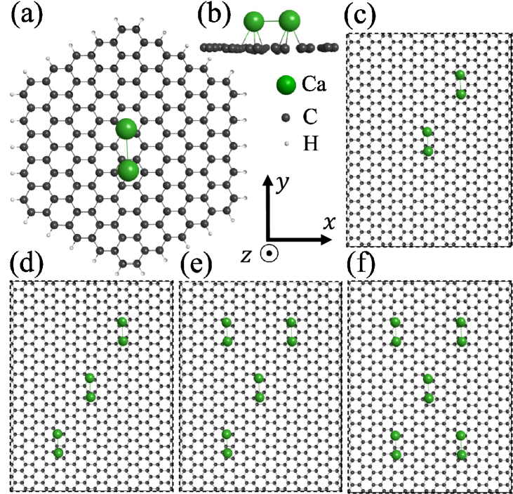
We carried out ab initio geometry relaxations based on DFT for a single calcium dimer on a honeycomb graphene lattice using the GAUSSIAN 09 software package with the PBEh1PBE hybrid function and the 6-31G** basis set PBE . For this purpose we adopted a graphene disk consisting of 150 carbon atoms passivated at the edges with 30 hydrogen atoms, the Ca dimer being bonded to the graphene disk at its center. Although a finite-size graphene cluster was used for the optimization calculations, the bond lengths between neighboring C atoms were well converged with increasing distance from the Ca, which indicates that the number of 150 C atoms is large enough to model the graphene monolayer. Since all of the atoms were allowed to relax freely, we found a maximum in-plane distortion of 0.02 Å between carbon atoms and a maximum out-of-plane distortion of 0.31 Å (away from the Ca) due to the presence of Ca dimer on the graphene. The final optimized geometry obtained in this study is shown in Fig. 1(a). The distance between the two Ca atoms of the dimer is 3.80 Å and the center of the dimer is located at 2.4 Å above the plane defined by the C atoms far from the Ca which is in agreement with the recent ab initio DFT calculations in a generalized gradient approximation for a Ca dimer adsorbed on graphene in supercells with periodic boundary conditions Wang . The positions of the Ca atoms in the graphene plane (relative to the center of the graphene disk) are , and , indicating that the Ca atoms are in nonequivalent positions.
Since the adsorbed Ca dimers on graphene behave as charged impurities, the electrostatic properties such as spatial charge distributions and electrostatic potentials at each atomic site should be computed by means of DFT calculations. For this reason, we designed a larger graphene hexagonal disk similar to that shown in Fig. 1(a) but with 1370 C atoms (not shown here). Then, we transferred the atomic coordinates of the relaxed Ca dimer along with those of the 54 closest C atoms surrounding the dimer and belonging to the optimized cluster in Fig. 1(a) to the locations of each of the Ca dimers of the larger disk to produce the structures with multiple Ca dimers shown in Fig.1(c)-(f). This procedure is justified since the distortion of the graphene lattice induced by an adsorbed Ca dimer has a shorter range than the distances between the Ca dimers in the clusters considered in this work (see Fig. 1(b)).The cluster geometries formed in this way were used to find the Mulliken atomic charges and the electric potentials on the carbon atoms of the graphene and the calcium atoms by means of DFT calculations.
The main difficulty in recognizing the physical resonant states induced by Ca dimers, especially at large distances from the dimer region where the influence of resonant states is not strong, is the mixing of these states with fluctuations in the electronic states around Dirac point energy due to edge effects in the model system. In order to suppress these quantum size effects as much as possible, a large rectangular graphene sheet (called here the “central ribbon”) consisting of 3940 carbon atoms with length 41.2 Å in the -direction and width 240 Å in the -direction was designed. Then all the relevant optimized coordinates and the atomic electrostatic potentials obtained from the DFT calculations for the 1370 C atom disk with adsorbed Ca dimers were applied to the appropriate atoms in this ribbon. Next, we attached two semi-infinite graphene ribbons (“leads” hereafter) with width 240 Å to the left and right sides of the central ribbon to produce an infinite ribbon (in the -direction) with width 240 Å. It is assumed that, the electrostatic potential values for all carbon atoms located far away from the dimers region converge to a fixed value. Therefore, for the remaining carbon atoms in the central ribbon and for all the atoms in the semi-infinite leads a cut-off in the electrostatic potential was used. A discussion of this point will be given in the next section.
According to the description given above, the Hamiltonian of the system which is partitioned in three blocks, i.e. the central ribbon and the two semi-infinite leads at its left and right sides, can be written as
| (1) |
where the Hamiltonians of the central ribbon, , and the leads, , are described by a tight-binding model derived from the extended Hückel theory in a basis of C and , and Ca and valence orbitals, that can be written as
| (2) |
where is the creation (annihilation) operator for an electron in the th atomic valence orbital . Within extended Hückel theory is the experimentally determined valence orbital ionization energy, and is the off-diagonal matrix element between valence orbitals and . In Eq. (1), describes the coupling matrix between the lead and the central ribbon . Since the basis set used in extended Hückel theory is nonorthogonal, the orbital overlap can be non-zero and will be included in this study Emberly1 ; Emberly2 . To include the atomic electrostatic potentials obtained from our DFT calculations in the present model, the diagonal and off-diagonal matrix elements in the Hamiltonians are modified as and where is the () component of the position of atom with orbital , and is the electric potential energy (EPE) for an atom at point . Note that the EPE values that will be discussed below, are the same for all valence orbitals localized on each given atom of the dimer-graphene system.
The Green’s function of the central ribbon coupled to the graphene leads can be written as Datta ; Saffar2010
| (3) |
where, with being a positive infinitesimal number, and are the self-energy terms due to the semi-infinite leads, each of which is considered as a semi-infinite stack of principal layers (ribbons) with nearest-neighbor interactions Lopez and can be defined as Nardelli12
| (4) |
where with being the overlap matrix between lead and the central ribbon . represents the surface Green’s function of the lead that can be written in terms of appropriate transfer matrices and computed using the iterative procedure introduced by López-Sancho et al. Lopez ; Nardelli12 ; Saffar2010 . Accordingly, we can calculate the local density of states (LDOS) for the th site in the central ribbon from the diagonal elements of as
| (5) |
Note that in all LDOS graphs that will be presented in this work, the average of LDOS associated with two neighboring carbon atoms in a single graphene unit cell is taken.
III Results and discussion
III.1 Mulliken charges and electrostatic potentials
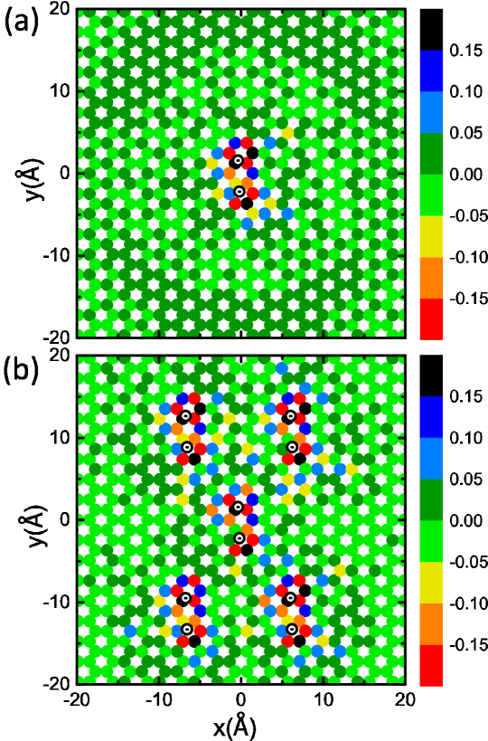
Adsorption of Ca dimers on the graphene plane results in a charge transfer between the Ca atoms of the dimers and the C atoms of the graphene. To explore the nature of this charge transfer and the polarity of charges, the Mulliken atomic charges were computed by DFT for all of the dimer-graphene clusters. The results for the case of one and five dimers are shown in Figs. 2(a) and 2(b), respectively. Figure 2 shows that electronic charge is transferred from the Ca dimers into graphene states and the calcium atoms become positively charged, in agreement with the experiment Wang . In addition, the negative localized charges, shown by light green circles around the single dimer in Fig. 2(a), form a stadium-shaped region similar to the charge density seen in the supplementary materials in Ref. Wang . From the charge distributions, it is obvious that the Mulliken atomic charges of the carbon atoms in the neighborhood of each single calcium atom are typically more negative than those of the carbon atoms far away from the dimers, screening the bare charges on calcium atoms. Some evidence of Friedel-like charge oscillations in the graphene is also visible, especially in Fig. 2(a). Importantly, increasing the number of dimers on the graphene sheet does not appreciably affect the negative-charge accumulations on the carbon atoms located in close vicinity to the Ca atoms, while in the case of a five-dimer structure, shown in Fig. 2(b), the concentration of negative charges on the carbon atoms away from the dimers is higher than for the one-dimer case in Fig. 2(a). The average charge transferred per Ca atom to the graphene depends on the number of dimers adsorbed on the graphene. From the calculated values of the Mulliken charges we found that as the number of dimers in a cluster was increased from one to five, the average charge transferred to the graphene per Ca atom in the cluster changes as -0.83, -0.72, -0.70, -0.69, and -0.69, respectively. That is, somewhat less than one electron per Ca atom is transferred to the graphene and the amount of charge transferred per Ca atom decreases as the number of Ca atoms in the cluster increases, as may be expected due to the repulsive nature of the interaction between the electrons transferred to the graphene.
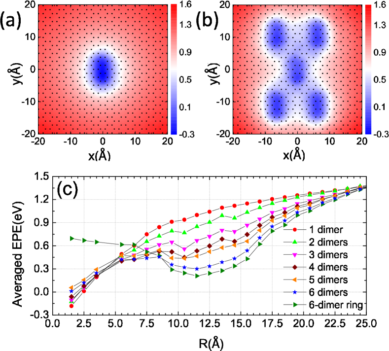
The spatial distributions of the EPE, , for two typical Ca-dimer clusters composed of one and five dimers are shown in Figs. 3(a) and 3(b). Here, is the charge of electron and is the difference between electric potential for an atom at point in the dimer-graphene cluster containing 1370 carbon atoms, and due to an atom of the same type as that at point in the cluster but in free space. is measured with respect to the center of each of the dimer-graphene clusters shown in Fig. 1. All of the electric potentials obtained from DFT were computed with the GAUSSIAN 09 package. Note that only the EPE at the sites of carbon atoms of the graphene are shown in Fig. 3. The EPE at the location of carbon atoms clearly reveals the influence of adsorbed dimers on the graphene in both one- and five-dimer clusters. The atomic sites with negative (positive) EPE values represent positive (negative) charges, which reflects the charge transfer from Ca dimers to carbon atoms of the graphene, as expected. For Å away from the dimers region in the direction, the EPE shows a convergence behavior due to the presence of screened charges on the Ca dimers. In order to get a better understanding of the behavior of EPE as a function of , we computed the average of EPE within each Å annulus for the dimer-graphene systems composed of 1-6 Ca dimers (a discussion for a six-dimer cluster and a six-dimer ring will be given in Section IIIC). The results are shown in Fig. 3(c). The averaged EPE, , for a single Ca dimer on graphene rises monotonically with distance from the cluster center, as expected for the screened Coulomb potential due to a positively charged dimer. As the number of Ca dimers increases from one to five the electric potential in the interval 5Å25Å becomes deeper due to the charge increase in the region of the dimers, which induces more quasi-bound states and stronger resonances in the electronic spectra of the dimer-graphene system. It is clear that the asymptotic behavior of is almost linear for small and large distances within the range shown in Fig. 3(c). For example, in the case of a cluster with a single Ca dimer, the expressions and ( is in units of eV and is in Å) can be fitted to the numerical results in the range of Åand 15ÅR25Årespectively.
The finite size of our 1370-carbon atom cluster used in the electrostatic potential calculations results in potential fluctuations at the edges of the cluster due to the presence of electronic states located at the edges. Accordingly, in the calculations reported below, we introduce a cutoff in the potential profile to lessen the influence of such edge effects as much as possible. The EPE cutoff value, chosen in all calculations that follow, is 1.2 eV.
III.2 Resonances in 1-5 Ca dimer clusters
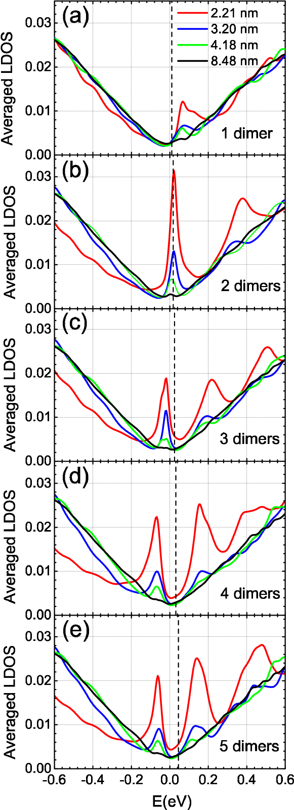
The inclusion of the electric potential in our calculations has crucial effects on the calcium-dimer-induced Dirac point resonant states of the graphene monolayer that will be studied here. Before presenting the main results for the LDOS, we should emphasize that the influence of carbon , , and orbitals on the electronic states for the dimer-graphene system was examined. A comparison of the resonances with and without the inclusion of these orbitals showed that the contribution of C , , and states to the energy and intensity of the resonances is very small and can be ignored in our calculation, indicating that the C orbitals make the main contribution in the emergence of the resonance states. Therefore, in the Hamiltonians given in Sec. II, only the C 2 orbitals are retained in the LDOS calculations. In addition, we shifted all of the electronic spectra to set the graphene Dirac point at zero energy. In the physical analysis of resonances, only the energy window close to the graphene Dirac point has been shown. The LDOS for graphene in the presence of Ca dimers at different lateral distances from the center of each dimer-graphene cluster (see Fig. 1) is shown in Figs. 4(a)-4(e). Note that in all clusters, the central dimer is the first Ca dimer that is placed on the graphene monolayer and the rest of the dimers surround it. All distances are measured from the center of the first Ca dimer. Figure 4(a) shows that in the case of one Ca dimer on the graphene layer, a weak resonance and oscillation appears in the energy window of the plot; the electronic states above the Fermi energy are affected the most by the presence of the Ca dimer. These Ca-related features decrease in strength with increasing distance from the Ca dimer (see the LDOS in Fig. 4(a) at 8.48 nm). The LDOS also displays an asymmetric behavior around the Dirac point energy that persists even at large distances from the Ca dimer, partly due to the inclusion of overlap matrix in our theory. In this study, to find the Fermi energy for each dimer-graphene system, the energy of highest occupied molecular orbital (HOMO) was first determined for the central graphene ribbon with and without Ca dimers. Then the difference between the two HOMO energies was added to the Dirac point energy as our estimate of the Fermi energy for the dimer-graphene system. This procedure was repeated for all of the dimer-graphene clusters. The electrochemical potential in the graphene leads was taken to be the Dirac point energy renormalized to match the Fermi energy as determined according to the above procedure.
In the case of the two-dimer cluster [Fig. 4(b)], the oscillation in the electronic LDOS above the Dirac point energy is stronger and has shifted downwards in energy. Moreover, the lowest energy resonant state is now partly populated with electrons, signaling that the atomic collapse is beginning to take place. This situation resembles the onset of atomic collapse in the STM experiments Wang , but corresponds to the case of four Ca dimers adsorbed on graphene in the experiment.
Possible reasons why the onset of atomic collapse occurred for a larger number of Ca dimers in the cluster in the experiment of Wang et al. Wang than in the present theory may include the following: In the experimentWang , the graphene layer was on a BN substrate, whereas in the present work, the calculations were carried out for suspended graphene in vacuum (with no substrate). Dielectric screening due to the substrate in the experiment is expected to reduce the strength of the Coulomb potential well induced in the graphene by the Ca dimers, thus requiring a larger number of adsorbed dimers for the atomic collapse to take place. The larger spatial separation between the Ca dimers in the experiment than in the present theory is also expected to result in a weaker Coulomb well in the experimental system, with qualitatively similar consequences.
As the number of Ca dimers increases from two to five [Fig. 4(b)-4(e)], the lowest resonant state becomes completely occupied and the number of quasi-bound states seen in the energy window in Fig.4 increases. In fact, a series of resonances develops which may be related to the Bohr-Sommerfeld quantization as was discussed in Ref. Shytov1 ; however, the resolution of the STM experiment Wang was only able to detect the lowest state. As can be seen in Fig. 4, the energy of the lowest atomic collapse state shifts below the graphene Dirac point as more dimers are added to the group, while the Fermi level moves up in energy. This means that additional charge transfer from Ca atoms to graphene occurs in the process of adsorbing each additional Ca dimer on the graphene monolayer.
In the experiment of Wang et al. Wang , a gaplike feature in normalized differential conductance was reported which comes from the effects of inelastic tunneling and the lifetime broadening by electron-phonon and electron-electron interactions Brar . Since we are only interested in studying the resonance features coming from the Ca dimers in suspended graphene LDOS, these effects have not been included in our calculations.
To examine the spatial dependence of the resonant states, the electronic LDOS were computed at different distances from the center of each dimer-graphene cluster. The results are presented in Fig. 4. Although the intensities of the resonances in the LDOS depend strongly on the distance from the center, the effect of resonances on the electronic spectra is still discernible even 8.48 nm from the center (the black curves in Fig. 4). This suggests that the resonant states are located mainly on the graphene as distinct from the localized atomic orbitals on Ca atoms.
To prove this point definitively, we removed the Ca atomic orbitals from the our model tight-binding Hamiltonian but retained the EPE values on the graphene that were obtained in our DFT calculations for the systems consisting of the graphene and adsorbed Ca dimers. In this way, only the effect of charge transfer between the Ca atoms and graphene on the graphene electric potentials was included in this test calculation, while the role of Ca valence orbitals was ignored. Interestingly, the results showed a negligible change in the electronic density of states when compared with the results in Fig. 4, showing that the presence of the resonance states is mainly due to the charge transfer from Ca dimers to graphene and not due to the hybridization between Ca and orbitals and graphene states.
III.3 Resonances in a 6-dimer cluster and ring
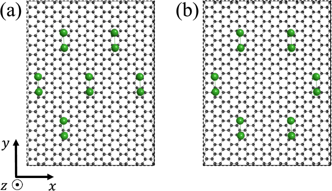
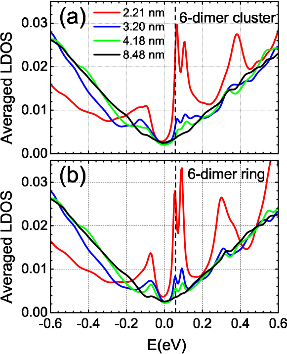
We explored the dependence of the Dirac point resonance features on the spatial arrangement of the Ca dimers adsorbed on the graphene by comparing the calculated LDOS for two different structures, each composed of six Ca dimers on the graphene monolayer. The dimer arrangements of the two structures considered are shown in Figs. 5(a) and 5(b). If we add two more dimers to the left and right side of the central dimer in Fig. 1(e), the six-dimer cluster of Fig. 5(a) is obtained. On the other hand, if the central dimer in Fig. 5(a) is shifted down along the diagonal, the 6-dimer ring shown in Fig. 5(b) is formed. The calculated local densities of states for the six-dimer cluster and the 6-dimer ring are shown in Figs. 6. The LDOS for the 6-dimer structures is based on the EPE values whose averages are shown in Fig. 3(c). The averaged EPE value for the six-dimer ring does not change significantly as a function of for Å. This is related to the absence of a central dimer in that structure and is a completely different behavior than what is seen in Fig. 3(c) for the other dimer-graphene clusters.
For both of the six-dimer structures the potential well in the range of Å is deeper than that for clusters composed of 1-5 Ca dimers, indicating more quasi-bound states for structures of this type. Figures 6(a) and 6(b) clearly show two distinct quasi-bound states near the Fermi level. Interestingly, the LDOS in the two arrangements shows that the second atomic-collapse state is becoming populated. We note that only a single atomic collapse resonance was observed to be populated in the STM experiment of Wang et al. Wang . However, Wang et al. Wang did not report any studies of six-dimer clusters. Although some of the the resonance features are somewhat narrower for the six-dimer ring than that for the six-dimer cluster in Fig. 6, it is evident that the energetic and spatial characteristics of the three lowest LDOS resonances are not affected greatly by the change in the arrangement of the dimers. The most significant difference between the LDOS for the two geometries is in the resonance energies above 0.2 eV at short distances (2.21 nm) from the center of clusters.
These results suggest that the adsorption of more Ca dimers on the graphene monolayer results in the transfer of more electric charge from Ca atoms to the graphene monolayer and a deeper electrostatic potential well in the graphene and that, accordingly, more atomic collapse states will be populated.
IV Conclusion
In summary, we have studied theoretically the Coulomb bound states and Dirac point resonances induced in a suspended graphene monolayer due to the adsorption of different number of Ca dimers on the graphene. We performed ab initio DFT calculations of the relaxed geometry for graphene with a single adsorbed Ca dimer and also the Mulliken atomic charges and the atomic electrostatic potentials for 1-6 Ca dimers on the suspended graphene. The tight-binding extended Hückel model, modified to include the electrostatic potentials obtained with DFT, was then used to compute the electronic structure of the system consisting of the adsorbed Ca atom dimers and the carbon atoms of the graphene monolayer. Our findings indicate that a charge transfer from dimers to the graphene occurs and increases as the number of dimers in the adsorbed cluster is increased from one to six.
Our calculated electronic structures reveal that the first atomic-collapse state close to the Dirac point energy begins to become populated with electrons when two Ca dimers are adsorbed on the suspended graphene. By contrast in the recent STM experiment Wang , the first atomic-collapse state was observed to begin to populate with electrons when four Ca dimers were present in the Ca cluster adsorbed on the graphene. Possible explanations of this difference may include dielectric screening of the Coulomb potential well in the graphene due to the BN substrate underlying the graphene monolayer in the experiment Wang and a shallower potential well due to the larger spacing between the Ca dimers in the experimental system.
Our theory also predicts a second atomic-collapse state to begin to populate with electrons when six Ca dimers are adsorbed on the suspended graphene. No studies involving adsorbed Ca clusters with six Ca dimers were reported by Wang et al.Wang . The experimental studyWang also only found evidence of a single atomic-collapse resonance becoming populated with electrons. Therefore, experiments testing our prediction of a second atomic-collapse state being populated with electrons for larger numbers of Ca dimers adsorbed on suspended graphene would be of interest. We note that suspended graphene monolayer nanostructures, although without adsorbed Ca dimers, have already been realized experimentally and their transport properties have been measured.Tombros11
The calculated spatial characteristics of the resonance features confirm that only the charge transfer from Ca atoms to graphene is responsible for the formation of the atomic-collapse resonances and that the local Ca valence orbitals are not involved significantly in the resonant states. Furthermore, it is found that the spatial arrangement of Ca dimers within the adsorbed dimer cluster does not strongly affect the formation of the atomic-collapse state and the location of quasi-bound states that are close in energy to the Dirac point, although the overall size of the Ca dimer cluster may be important. These findings can be used in future nanoscale devices where there is a need to confine electrical charges to a small area.
This work was supported by NSERC, CIFAR, WestGrid, and Compute Canada.
References
- (1) K.S. Novoselov, A.K. Geim, S.V. Morozov, D. Jiang, M.I. Katsnelson, I.V. Grigorieva, S.V. Dubonos, and A.A. Firsov, Nature (London) 438, 197 (2005); Y. Zhang, Y.-W. Tan, H.L. Stormer, and P. Kim, Nature (London) 438, 201 (2005); A.K. Geim and K.S. Novoselov, Nat. Mater. 6, 183 (2007); A.K. Geim, Science 324, 1530 (2009).
- (2) P.R. Wallace, Phys. Rev. 71, 622 (1947).
- (3) A.H. Castro Neto, F. Guinea, N.M.R. Peres, K.S. Novoselov, and A.K. Geim, Rev. Mod. Phys. 81, 109 (2009).
- (4) V.M. Pereira, J. Nilsson, and A.H. Castro Neto, Phys. Rev. Lett. 99, 166802 (2007).
- (5) A.V. Shytov, M.I. Katsnelson, and L.S. Levitov, Phys. Rev. Lett. 99, 236801 (2007).
- (6) A.V. Shytov, M.I. Katsnelson, and L.S. Levitov, Phys. Rev. Lett. 99, 246802 (2007).
- (7) M.M. Fogler, D.S. Novikov, and B.I. Shklovskii, Phys. Rev. B 76, 233402 (2007).
- (8) Y. Wang, V.W. Brar, A.V. Shytov, Q. Wu, W. Regan, H.-Z. Tsai, A. Zettl, L.S. Levitov, and M.F. Crommie, Nat. Phys. 8, 653 (2012).
- (9) T. Ando, J. Phys. Soc. Jpn. 75, 074716 (2006).
- (10) K. Nomura and A.H. MacDonald, Phys. Rev. Lett. 98, 076602 (2007).
- (11) E. H. Hwang, S. Adam, and S. Das Sarma, Phys. Rev. Lett. 98, 186806 (2007).
- (12) S. Ihnatsenka and G. Kirczenow, Phys. Rev. B 83, 245442 (2011).
- (13) G. Kirczenow and S. Ihnatsenka, Ch. 13 in Graphene Nanoelectronics: Metrology, Synthesis, Properties and Applications edited by H. Raza (Springer, Heidelberg, Dordercht, London, New York, 2012).
- (14) F. Schedin, A.K. Geim, S.V. Morozov, D. Jiang, E.H. Hill, P. Blake, and K.S. Novoselov, Nat. Mater. 6, 652 (2007)
- (15) E. H. Hwang, S. Adam, and S. Das Sarma, Phys. Rev. B 76, 195421 (2007).
- (16) T.O. Wehling, K.S. Novoselov, S.V. Morozov, E.E. Vdovin, M.I. Katsnelson, A.K. Geim, and A.I. Lichtenstein, Nano Lett. 8, 173 (2008).
- (17) T. Ohta, A. Bostwick, T. Seyller, K. Horn, and E. Rotenberg, Science 315, 951 (2006).
- (18) B. Uchoa, C.-Y. Lin, and A. H. Castro Neto, Phys. Rev. B 77, 035420 (2008).
- (19) Y. Mao, J. Yuan, and J. Zhong, J. Phys: Condens. Matter 20, 115209 (2008).
- (20) K. T. Chan, J. B. Neaton, and M. L. Cohen, Phys. Rev. B 77, 235430 (2008).
- (21) T.O. Wehling, A.V. Balatsky, M.I. Katsnelson, A.I. Lichtenstein, and A. Rosch, Phys. Rev. B 81, 115427 (2010).
- (22) T. O. Wehling, H. P. Dahal, A. I. Lichtenstein, M. I. Katsnelson, H. C. Manoharan, and A. V. Balatsky, Phys. Rev. B 81, 085413 (2010).
- (23) C. Cao, M. Wu, J. Jiang, and H.-P. Cheng, Phys. Rev. B 81, 205424 (2010).
- (24) D. Jacob and G. Kotliar, Phys. Rev. B 82, 085423 (2010).
- (25) K.T. Chan, H. Lee, and M.L. Cohen, Phys. Rev. B 83, 035405 (2011).
- (26) T. G. Rappoport, M. Godoy, B. Uchoa, R. R. dos Santos and A. H. Castro Neto, Eurphys. Lett. 96, 27010 (2011).
- (27) T. O. Wehling, A. I. Lichtenstein, M. I. Katsnelson, Phys. Rev. B 84, 235110 (2011).
- (28) X. Liu, C. Z. Wang, Y. X. Yao, W. C. Lu, M. Hupalo, M. C. Tringides, and K. M. Ho, Phys. Rev. B 83, 235411 (2011).
- (29) A. Saffarzadeh and G. Kirczenow, Phys. Rev. B 85, 245429 (2012).
- (30) Y. Wang, D. Wong, A.V. Shytov, V.W. Brar, S. Choi, Q. Wu, H.-Z. Tsai, W. Regan, A. Zettl, R.K. Kawakami, S.G. Louie, L.S. Levitov, M.F. Crommie, Nature Materials 340, 734 (2013).
- (31) For a recent review, see G. Kirczenow, in The Oxford Handbook of Nanoscience and Technology, Volume I: Basic Aspects, edited by A. V. Narlikar and Y. Y. Fu, Chap. 4 (Oxford University Press, Oxford, 2010).
- (32) J.H. Ammeter, H.B. Buergi, J.C. Thibeault, and R. Hoffmann, J. Am. Chem. Soc. 100, 3686 (1978).
- (33) The YAEHMOP code implementation of the extended Hückel theory (Ref. Ammeter ) by G. A. Landrum and W. V. Glassey (Source-Forge, Fremont, CA, 2001) was used. YAEHMOP does not include spin effects.
- (34) M. Ernzerhof and J. P. Perdew, J. Chem. Phys. 109, 3313 (1998).
- (35) E. Emberly and G. Kirczenow, Phys. Rev. Lett. 81, 5205 (1998).
- (36) E. Emberly and G. Kirczenow, J. Phys. Condens. Matter 11, 6911 (1999).
- (37) S. Datta, Quantum Transport: Atom to Transistor (Cambridge University Press, Camberige, 2005).
- (38) A. Saffarzadeh, J. Appl. Phys. 107, 114309 (2010).
- (39) M.P. López-Sancho, J.M. López-Sancho and J. Rubio, J. Phys. F: Met. Phys. 14, 1205 (1984); 15, 851 (1985).
- (40) M. Buongiorno Nardelli, Phys. Rev. B 60, 7828 (1999); M. Buongiorno Nardelli and J. Bernholc, Phys. Rev. B 60, R16 338 (1999).
- (41) V.W. Brar, S. Wickenburg, M. Panlasigui, C.-H. Park, T.O. Wehling, Y. Zhang, R. Decker, Ç. Girit, A.V. Balatsky, S.G. Louie, A. Zettl, and M.F. Crommie, Phys. Rev. Lett. 104, 036805 (2010).
- (42) N. Tombros, A. Veligura, J. Junesch, M. H. D. Guimaraes, I. J. Vera-Marun, H. T. Jonkman and B. J. van Wees, Nature Physics 7, 697 (2011).