DFT+U simulation of the Ti4O7-TiO2 interface
Abstract
The formation of conducting channels of Ti4O7 inside TiO2-based memristors is believed to be the origin for the change in electric resistivity of these devices. While the properties of the bulk materials are reasonably known, the interface between them has not been studied up to now mostly due to their different crystalline structures. In this work we present a way to match the interfaces between TiO2 and Ti4O7 and subsequently the band offset between these materials is obtained from density functional theory based calculations. The results show that while the valence band is located at the Ti4O7, the conduction band is found at the TiO2 structure, resulting into a type II interface. In this case, the Ti4O7 would act as a donor to the TiO2 matrix.
I Introduction
The memristor is an electronic device predicted by L. Chua in 1971chua_1971 ; chua_kang_1976 and experimentally obtained a few years ago.S_Williams_nature_2008 These devices are characterized by distinct resistance states which could be used to store information as they show very fast switching and high retention times.Jeong2012
There are reports of a wide range of materials (particularly metal oxides) which show this memristive effect.choi2005 ; Syu2013 ; Wang2013 ; Kim2013a ; Huang2013 ; Kim2013b ; He2013 ; Ignatiev2006 ; Guo2013 ; Pilch2014 Although the switching mechanism, and the origin of the different resistance states has not been completely elucidated, it is generally believed that the presence of oxygen deficient phases plays a major role in the memristive effect.Szot2011 Within the possible materials, TiO2 is one of the most studied ones.Szot2011 ; Kim2011 ; Janotti2010 ; choi2005 ; Jeong2008 ; Kwon2010 Inside memristive devices, Ti4O7 channels immersed in the TiO2-based matrix have been observed, and the formation of such structures is believed to be largely responsible for the change in resistivity.Kwon2010
While TiO2 is known to be a wide gap semiconductor (experimental band gap eVAmtout1995 ) Ti4O7 presents three phases with different electronic transport properties. The low temperature ( 140 K) and intermediate temperature phases (140 K 150 K) are semiconductors while the high temperature phase ( 150 K) is metallic.Bartholomew1969 ; Marezio1971 ; Marezio1973 ; LePage1984 The differences between those phases is mainly due to small atomic displacements which do not lead to significant changes in the unit cell.
Despite the large amount of theoretical work on either TiO2 rutile Cho2006 ; Iddir2007 ; Li2009a ; Janotti2010 and Ti4O7,Eyert2004 ; Leonov2006 ; Liborio2009 ; Weissmann2011 ; Padilha2014a the band alignment of these two materials is not known up to now, mainly because of the difficulty in building a supercell containing the Ti4O7-TiO2 interface - the two materials present very different unit cells, making the match between them very difficult. This information could be very useful to the understanding of the atomic level mechanism of the memristor, given that the Ti4O7-TiO2 interface spans a great part of the device length after the formation of the conducting channels.
As the total energy is given with respect to an arbitrary reference energy in periodic calculations, a common reference should be determined for all the structures involved in this work.Ihm1979 In fact, the knowledge of this common reference is necessary to find the offset between the valence band of different materials. The knowledge of this band offset is important, for instance, in determining whether there is charge transfer at the interface between the two systems, the materials doping limitsZhang2000 as well as other properties. For instance, Scanlon et al.Scanlon2013 determined the band offset between rutile and anatase TiO2 structures via a cluster approach, providing an understanding about the separation of charge carriers in photocatalysis using the mixed-phase structure.
Our objective in this paper is to study the interface of TiO2 and one of its oxygen deficient counterparts, Ti4O7. For this purpose, we built a supercell containing the Ti4O7-TiO2 interface which was then used for our calculations. In particular we analyze the band alignment, which has been found to be of type II (the conduction band minimum (CBM) is located in one material and valence band maximum (VBM) in the other), and its consequences to the overall electronic structure of the combined system.


II Computational Details
All density functional theory (DFTHohenberg_Kohn_64 ; Kohn_Sham_65 ) calculations in this work were performed using the VASP package.Kresse1996 ; KresseFurthmuller1996 Wave functions are described within the Projector Augmented Waves (PAW) schemeBlochl1994 ; Kresse1999 with periodic boundary conditions. The and electrons were considered as valence electrons for Ti and O atoms respectively and the PBE functionalPerdew1997 was used as the exchange-correlation potential. The cutoff energy for the plane wave expansion was 700 eV and the k-point meshes used throughout this work were generated using a -centered grid. Spin polarization was taken into account for all calculations. Relaxation of the ions was performed while the unit cell was kept fixed, until forces were smaller than eV/Å, for the isolated materials and eV/Å, for the supercell. We have performed test calculations with a smaller supercell for the interface, but with more strict parameters for the convergence of the forces. The results were similar for quantities calculated in this work.
A Hubbard parameter was introduced for a better description of the Ti(d) electrons. Our earlier work Padilha2014a shows that a value of 5 eV for is enough to achieve a good description of the electronic structure of TinO2n-1 () Magnéli phases. Even though, test calculations were performed for other values of (0, 2 and 4 eV) and the same qualitative results were obtained for the type of alignment as well as the relative position of the unnocupied levels of the same materials. In the rotationally invariant scheme as implemented in VASPDudarev only the value of ( is the spherically averaged matrix element of the screened Coulomb interaction between electrons) is of relevance, thus was set to zero for all calculations.
III Construction of the Interface
One of the key points in this work is that building the interface requires matching two of the three unit cell vectors of each compound at the interfacial region. For that to be accomplished, it is necessary to find the smallest supercell where the deformation imposed to each compound is such that no significant change in electronic structure with respect to the bulk material arises in regions away from the interface. For the materials presented in this work, this is difficult, since the TiO2 and the Ti4O7 presented very distinct unit cells. The stable form of TiO2 at ambient conditions is the rutile structure (tetragonal unit cell, Å, ÅGrant1959 ) while the Ti4O7 presents a complicated Magnéli structure (triclinic cell, see Table 1).
| HT | IT | LT | TR | |
|---|---|---|---|---|
| (Å) | 5.60 | 5.60 | 5.63 | 5.46 |
| (Å) | 7.12 | 7.13 | 7.20 | 7.14 |
| (Å) | 20.43 | 20.36 | 20.26 | 20.70 |
| (o) | 67.70 | 67.76 | 67.90 | 65.52 |
| (o) | 57.16 | 57.44 | 57.69 | 57.22 |
| (o) | 108.76 | 109.02 | 109.68 | 108.46 |
To overcome this difficulty, we followed steps that lead to the derivation of the Magnéli structure from the rutile one as follows. The first step is to obtain the Magnéli phase structures from TiO2 rutile via the unit cell transformationWood1981
| (1) |
where and are the unit cell vectors of the Magnéli structure of index . The result of using this operation for the case when is illustrated in Fig. 1(b) and the comparison with the Ti4O7 unit cell is presented in Table 1. Notice that this still represents a TiO2 rutile structure, but the unit cell is now the one from Ti4O7. From this point, the Ti4O7 Magnéli phase, as well as all Magnéli phases (TinO2n-1, ) can be generated via the operationAndersson1960 ; Harada2010 ; Anderson19671393
| (2) |
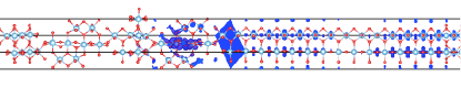
that consists of periodic displacements; after every -th (121) plane, the atoms are translated by crystal vector of the rutile unit cell. This operation leads to the formation of extended defects, which are composed of oxygen vacancies (’s) restricted to planes known as shear planes. The resulting arrangement is presented in Fig. 1(a). Since the operation given by equation 2 affects only the atomic positions, both structures present the same triclinic unit cell.
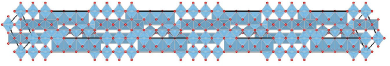
In essence, the transformation presented above results in unit cells with equal lengths. The two materials can thus be interfaced in the plane that is secant to the axis (highlighted in Fig. 1(c)). This Ti4O7-TiO2 interface is, by construction, strain free, defect free, presents exactly the same cell parameters and consequently no dipoles would arise at the heterojunction. In our calculations we created a supercell along the axis by repeating the cell for each material four times (Å) in order to ensure convergence of the potential away from the interface.
IV Band Offset
After obtaining the three structures - both isolated materials and their interface - it is possible to calculate the natural band offset between the two systems studied in this work. The band offset will be given by Li2009b
| (3) |
where and are the differences between the Valence Band Maximum energy () and the electrostatic potential averaged over a certain volume of the unit cell of the isolated materials, while is the difference between the averaged electrostatic potential of the different materials calculated in bulk-like regions of the relaxed heterostructure supercell.
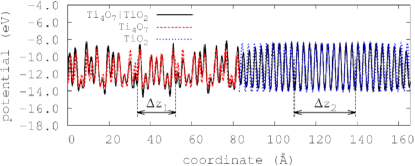
The determination of the quantities needed by equation 3 can be achieved by, first, obtaining the electronic structure of each isolated (bulk) system. From this calculation, the average electrostatic potential along the crystal axis which is secant to the interface (the axis, in this case) is determined,
| (4) |
as well as the position in energy of the VBM, for each system. Using the heterostructure after ionic relaxation we also calculated in a similar fashion. From the plot of the electrostatic potential for all three structures (shown in figure 2) it is possible to define regions, labeled and , where both the bulk materials and the heterostructure present similar characteristics. These regions of the heterostructure are considered as bulk-like and should have, in principle, the same potential. The average electrostatic potential is then obtained by the integration of along and for Ti4O7 and TiO2 respectively, and is used to calculate the first and second terms of equation 3. From the heterostructure calculation, the same quantities are used to obtain the final term.
The third step would comprise the determination of the band energy shift due to the hydrostatic pressure. In this particular case our heterostructure is completely strain free, as it is built by equal unit cells, thus this last step presents no contribution. After those steps were carried out, the band offset obtained in our case resulted in eV. Numerical errors due to the choice of a particular were estimated to be 0.3 eV, by comparison with other test calculations performed using other values of . Even though the value of the valence band offset presented a variation with respect to the value of used, being smaller for smaller , the overall electronic structure of the interface has not changed, and the final result, which is the relative position of electronic levels of TiO2 and Ti4O7, remained practically unchanged. For this reason, we have chosen to report only the results for = 5 eV.
V Results
The projected Density of States (PDOS) was calculated for the two isolated structures and the results were shifted in energy by the band offset. These results are shown in fig. 3. From that graph, it is possible to notice that the VBM of the interface is located on Ti4O7, while the CBM is found in the TiO2, resulting in a type II heterostructure.
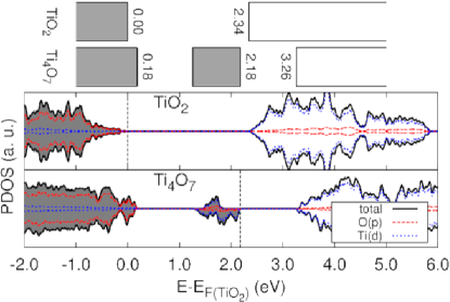
Given that the CBM is 0.16 eV above the VBM (upper panel, Fig. 3), it is possible that electrons would leave the Ti4O7 structure and arrive at the unoccupied levels at the TiO2 structure due to the presence of an electric field. In this case, the Ti4O7 channels present inside of the TiO2 matrix that forms the memristor could act as donors to the neighboring region of that matrix. This specific characteristic does not depend on the choice of . While it is known that the isolated oxygen vacancy in the TiO2 rutile acts as a shallow donor,Janotti2010 as to our knowledge, this same behavior has not been reported for the ordered defects present into the Ti4O7 structure.
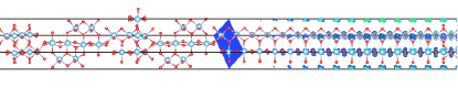
Further evidence of the real-space separation of the VBM and CBM is given by the projected charge density over the frontier orbitals. The projection was performed for the last occupied and first unoccupied bands, at the point. As a result, presented in Fig. 4, it is possible to notice that while the VBM (Fig 4(b)) is located mainly on the Ti atoms of the Ti4O7 structure close to the interface (with a contribution of some of the Ti atoms from TiO2), the CBM (Fig. 4(a)) is located exclusively on the TiO2 segment.
Some hybridization may be responsible for the contribution coming from the TiO2 structure to the VBM, as both levels present Ti(d) character (see Fig 3). Another explanation for this contribution would be the length of the axis, which is not long enough to describe the separation of the frontier orbitals. Indeed, calculations performed with a smaller supercell (the supercell vector length was half of the one used in the calculations presented) resulted in larger charge delocalization. Therefore, we expect that, in the limit of longer unit cells (closer to realistic systems) the charge would be fully separated on the two phases.
VI Conclusions
In conclusion, we have reported the band offset given by the average of the electrostatic potential for the Ti4O7-TiO2 heterostructure. The supercell containing the junction was built using transformations that resulted in the same unit cell for both materials present on this junction. The localization of the VBM and CBM was determined to be at the Ti4O7 and TiO2 structures respectively, resulting in a type II heterostructure. As the band gap is 0.16 eV, our results indicate that the Ti4O7 channels inside of the memristor TiO2 matrix would then act as donors for the TiO2 structure.
Acknowledgements.
This work was supported by FAPESP, and CNPq. The support given by Cenapad-SP in the form of computational infrastructure is also acknowledged.References
- (1) Leon O. Chua, Memristor-the missing circuit element, IEEE Trans. Circ. Theo. CT-18, 507 – 519 (1971).
- (2) Leon O. Chua and S. M. Kang, Memristive devices and systems, Proc. IEEE 64, 209 – 223 (1976).
- (3) D. B. Strukov, G. S. Snider, D. R. Stewart, and R. S. Williams, The missing memristor found, Nature 453, 80 – 83 (2008).
- (4) D. S. Jeong, R. Thomas, R. S. Katiyar, J. F. Scott, H. Kohlstedt, A. Petraru, and C. S. Hwang, Emerging memories: resistive switching mechanisms and current status, Rep. progr. Phys. 75, 076502 (2012).
- (5) B. J. Choi, D. S. Jeong, S. K. Kim, C. Rohde, S. Choi, J. H. Oh, H. J. Kim, C. S. Hwang, K. Szot, R. Waser, B. Reichenberg, and S. Tiedke, Resistive switching mechanism of TiO2 thin films grown by atomic-layer deposition, J. Appl. Phys. 98, 033715 (2005).
- (6) Y-E. Syu, T-C. Chang, J-H. Lou, T-M. Tsai, K-C. Chang, M-J. Tsai, Y-L. Wang, M. Liu, and S. M. Sze, Atomic-level quantized reaction of HfOx memristor, Appl. Phys. Lett. 102, 172903 (2013).
- (7) X. L. Wang, P. S. Ku, Q. Shao, W. F. Cheng, C. W. Leung, and A. Ruotolo, Magnetism as a probe of the origin of memristive switching in p-type antiferromagnetic NiO, Appl. Phys. Lett. 103, 223508 (2013).
- (8) J-D. Kim, Y-J. Baek, Y. Jin Choi, C. Jung Kang, H. Ho Lee, H-M. Kim, K-B. Kim, and T-S. Yoon, Investigation of analog memristive switching of iron oxide nanoparticle assembly between Pt electrodes, J. Appl. Phys. 114, 224505 (2013).
- (9) C-H. Huang, J-S. Huang, C-C. Lai, H-W. Huang, S-J. Lin, and Y-L. Chueh, Manipulated transformation of filamentary and homogeneous resistive switching on ZnO thin film memristor with controllable multistate, ACS Appl. Mat. & Interf. 5, 6017–23 (2013).
- (10) J. Kim, K. Lee, Y. Kim, H. Na, D-H. Ko, H. Sohn, and S. Lee, Effect of thermal annealing on resistance switching characteristics of Pt/ZrO2/TiN stacks, Mat. Chem. Phys. 142, 608–613 (2013).
- (11) X. He, Y. Yin, J. Guo, H. Yuan, Y. Peng, Y. Zhou, D. Zhao, K. Hai, W. Zhou, and D. Tang, Memristive properties of hexagonal WO3 nanowires induced by oxygen vacancy migration, Nanosc. Res. Lett. 8, 50 (2013).
- (12) A. Ignatiev, N. J. Wu, X. Chen, S. Q. Liu, C. Papagianni, and J. Strozier, Resistance switching in perovskite thin films, Phys. Stat. Sol. (B) 243, 2089–2097 (2006).
- (13) Z. Guo, B. Sa, J. Zhou, and Z. Sun, Role of oxygen vacancies in the resistive switching of SrZrO3 for resistance random access memory, J. Alloys Comp. 580, 148–151 (2013).
- (14) M. Pilch and A. Molak, Resistivity switching induced in ferroelectric phase of PbTiO3 studied by XPS and electric conductivity tests, J. Alloys Comp. 586, 488–498 (2014).
- (15) K Szot, M Rogala, W Speier, Z Klusek, a Besmehn, and R Waser, TiO2–a prototypical memristive material, Nanotechnology 22, 254001 (2011).
- (16) K. M. Kim, D. S. Jeong, and C. S. Hwang, Nanofilamentary resistive switching in binary oxide system; a review on the present status and outlook, Nanotechnology 22, 254002 (2011).
- (17) A. Janotti, J. B. Varley, P. Rinke, N. Umezawa, G. Kresse, and C. G. Van de Walle, Hybrid functional studies of the oxygen vacancy in TiO2, Phys. Rev. B 81, 085212 (2010).
- (18) D. S. Jeong, H. Schroeder, U. Breuer, and R. Waser, Characteristic electroforming behavior in Pt/TiO2/Pt resistive switching cells depending on atmosphere, J. Appl. Phys. 104, 123716 (2008).
- (19) D.-H. Kwon, K. M. Kim, J. H. Jang, J. M. Jeon, M. H. Lee, G. H. Kim, X.-S. Li, G.-S. Park, B. Lee, S. Han, M. Kim, and C. S. Hwang, Atomic structure of conducting nanofilaments in TiO2 resistive switching memory, Nature Nanotech. 5, 148 – 153 (2010).
- (20) A. Amtout and R. Leonelli, Optical properties of rutile near its fundamental band gap, Phys. Rev. B 51, 6842–6851 (1995).
- (21) R. Bartholomew and D. Frankl, Electrical Properties of Some Titanium Oxides, Phys. Rev. 187, 828–833 (1969).
- (22) M. Marezio and P.D. Dernier, The crystal structure of Ti4O7, a member of the homologous series TinO2n−1, J. Sol. State Chem. 3, 340–348 (1971).
- (23) M. Marezio, D.B. McWhan, P.D. Dernier, and J.P. Remeika, Structural aspects of the metal-insulator transitions in Ti4O7, J. Sol. State Chem. 6, 213–221 (1973).
- (24) Y. Le Page and M. Marezio, Structural chemistry of Magnéli phases TinO2n−1 (4 ≤ n ≤ 9), J. Sol. State Chem. 53, 13–21 (1984).
- (25) E. Cho, S. Han, H-S. Ahn, K-R. Lee, S. Kim, and C. Hwang, First-principles study of point defects in rutile TiO2−x, Phys. Rev. B 73, 193202 (2006).
- (26) H. Iddir, S. Ögüt, P. Zapol, and N. D. Browning, Diffusion mechanisms of native point defects in rutile TiO2: Ab initio total-energy calculations, Phys. Rev. B 75, 073203 (2007).
- (27) X. Li, M.W. Finnis, J. He, R.K. Behera, S.R. Phillpot, S.B. Sinnott, and E.C. Dickey, Energetics of charged point defects in rutile TiO2 by density functional theory, Acta Mat. 57, 5882–5891 (2009).
- (28) V. Eyert, U. Schwingenschlögl, and U. Eckern, Charge order, orbital order, and electron localization in the Magnéli phase Ti4O7, Chem. Phys. Lett. 390, 151–156 (2004).
- (29) I. Leonov, a N. Yaresko, V. N. Antonov, U. Schwingenschlögl, V. Eyert, and V. I. Anisimov, Charge order and spin-singlet pair formation in Ti4O7, J. Phys. Cond. Mat. 18, 10955–10964 (2006).
- (30) L. Liborio, G. Mallia, and N. Harrison, Electronic structure of the Ti4O7 Magnéli phase, Phys. Rev. B 79, 245133 (2009).
- (31) M. Weissmann and R. Weht, Electronic and magnetic properties of the different phases of Ti4O7 from density functional theory, Phys. Rev. B 84, 144419 (2011).
- (32) A. C. M. Padilha, J. M. Osorio-Guillén, A. R. Rocha, and G. M. Dalpian, TinO2n−1 Magnéli phases studied using density functional theory, Phys. Rev. B 90, 035213 (2014).
- (33) J. Ihm, A. Zunger, and M. L. Cohen, Momentum-space formalism for the total energy of solids, J. Physics C 12, 4409–4422 (1979).
- (34) S. B. Zhang, S.-H. Wei, and Alex Zunger, Microscopic Origin of the Phenomenological Equilibrium “Doping Limit Rule” in n-Type III-V Semiconductors, Phys. Rev. Lett. 84, 1232–1235 (2000).
- (35) D. O. Scanlon, C. W. Dunnill, J. Buckeridge, S. A. Shevlin, A. J. Logsdail, S. M. Woodley, C. R. A. Catlow, M. J. Powell, R. G. Palgrave, I. P. Parkin, G. W. Watson, T. W. Keal, P. Sherwood, A. Walsh, and A. A. Sokol, Band alignment of rutile and anatase TiO2, Nature Mat. 12, 798–801 (2013).
- (36) P. Hohenberg and W. Kohn, Inhomogeneous Electron Gas, Phys. Rev. 136, B864–B871 (1964).
- (37) W. Kohn and L. J. Sham, Self-Consistent Equations Including Exchange and Correlation Effects, Phys. Rev. 140, A1133–A1138 (1965).
- (38) G. Kresse, Efficiency of ab-initio total energy calculations for metals and semiconductors using a plane-wave basis set, Comp. Mat. Sci. 6, 15–50 (1996).
- (39) G. Kresse and J. Furthmüller, Efficient iterative schemes for ab initio total-energy calculations using a plane-wave basis set, Phys. Rev. B 54, 11169–11186 (1996).
- (40) P. E. Blöchl, Projector augmented-wave method, Phys. Rev. B 50, 17953–17979 (1994).
- (41) G. Kresse and D. Joubert, From ultrasoft pseudopotentials to the projector augmented-wave method, Phys. Rev. B 59, 1758–1775 (1999).
- (42) J. P. Perdew, K. Burke, and M. Ernzerhof, Generalized Gradient Approximation Made Simple [Phys. Rev. Lett. 77, 3865 (1996)], Phys. Rev. Lett. 78, 1396–1396 (1997).
- (43) S. L. Dudarev, G. A. Botton, S. Y. Savrasov, C. J. Humphreys, and A. P. Sutton, Electron-energy-loss spectra and the structural stability of nickel oxide: An LSDA+U study, Phys. Rev. B 57, 1505–1509 (1998).
- (44) F. Grant, Properties of Rutile (Titanium Dioxide), Rev. Mod. Phys. 31, 646–674 (1959).
- (45) G. J. Wood and L. A. Bursill, The Formation Energy of Crystallographic Shear Planes in TiO, Proc. R. Soc. A 375, 105–125 (1981).
- (46) S. Andersson, D. H. Templeton, S. Rundqvist, E. Varde, and G. Westin, The Crystal Structure of Ti5O9, Acta Chem. Scand. 14, 1161–1172 (1960).
- (47) S. Harada, K. Tanaka, and H. Inui, Thermoelectric properties and crystallographic shear structures in titanium oxides of the Magnéli phases, J. Appl. Phys. 108, 083703 (2010).
- (48) J.S. Anderson and B.G. Hyde, On the possible role of dislocations in generating ordered and disordered shear structures, J. Phys. Chem. Sol. 28, 1393 – 1408 (1967).
- (49) Y-H. Li, A. Walsh, S. Chen, W-J. Yin, J-H. Yang, J. Li, J. L. F. Da Silva, X. G. Gong, and S-H. Wei, Revised ab initio natural band offsets of all group IV, II-VI, and III-V semiconductors, Appl. Phys. Lett. 94, 212109 (2009).