The formation of the positive, fixed charge at c-Si(111)/a-Si3N3.5:H interfaces
Abstract
Modern electronic devices are unthinkable without the well-controlled formation of interfaces at heterostructures. These often involve at least one amorphous material. Modeling such interfaces poses a significant challenge, since a meaningful result can only be expected by using huge models or by drawing from many statistically independent samples. Here we report on the results of high throughput calculations for interfaces between crystalline silicon (c-Si) and amorphous silicon nitride (a-Si3N3.5:H), which are omnipresent in commercially available solar cells. The findings reconcile only partly understood key features. At the interface, threefold coordinated Si atoms are present. These are caused by the structural mismatch between the amorphous and crystalline part. The local Fermi level of undoped c-Si lies well below that of a-SiN:H. To align the Fermi levels in the device, charge is transferred from the a-SiN:H part to the c-Si part resulting in an abundance of positively charged, threefold coordinated Si atoms at the interface. This explains the existence of a positive, fixed charge at the interface that repels holes.
I Motivation
Silicon is the most important material for single-junction solar cells. Although there are other promising compounds for photo voltaic devices such as GaAs, CdTe, or InP, silicon based cells still maintain about % market share Luque and Hegedus (2011); Abou-Ras et al. (2011). Silicon has the advantage of being widely available, non-toxic, and applicable to many different requirements. The possible applications range from less efficient, but cheap, amorphous cells over cost-efficient multi-crystalline cells up to highly efficient, but more expensive, mono-crystalline cells Luque and Hegedus (2011); Green et al. (2012). To produce high performance cells, optical losses must be minimized and recombination centers passivated. Meeting both challenges, amorphous silicon nitride (a-SiN:H) is commonly deposited as anti-reflection and passivation layer on top of crystalline silicon (c-Si) solar cells with p-type base and n-type emitter. Using plasma enhanced chemical vapor deposition (PECVD) Aberle (2000); Duerinckx and Szlufcik (2002), the deposition parameters (i.e. the gas mixture of N2/SiH3 or NH3/SiH3) control the refractive index as well as the defect concentration of a-Si3Nx:H so that the reflectivity and the passivation can be tuned for optimal cell performance.
However, even with high quality surface passivation, the defect concentration at interfaces is larger than in bulk materials, and defect assisted Shockley-Read-Hall (SRH) recombination remains a major source of carrier losses in solar cells Shockley and Read (1952); Hall (1952). Especially, defect levels in the middle of the Si band gap are effective recombination centers and carrier traps. They reduce the lifetime of electron-hole pairs in c-Si and, therewith, the efficiency of the solar cells Bube (1983); Green (1986). Lamers et al. showed that the defect density correlates with what is called the ”fixed charge” Lamers et al. (2012). This fixed charge is positive and located at the c-Si/a-SiN:H interface. In contrast to charge neutral recombination centers, the fixed charge increases the lifetime of charge carriers in n-type doped c-Si by repelling holes from the interface. As undercoordinated Si atoms can have negative, neutral, or positive charge (i.e. K-, K0, or K+ defects), the fixed charge is typically explained by an increased number of K+ defects at the interface Aberle (2001). However, it is still unclear how those defects form and whether one could also produce c-Si/a-SiN:H interfaces with a negative, fixed charge that repels electrons and attracts holes. It is therefore obvious that defects are important to understand the properties of c-Si/a-SiN:H interfaces. Nonetheless, they are very difficult to investigate by experimental methods alone. For instance, lifetime measurements estimate defect concentrations indirectly, and electron spin resonance (ESR) measurements can solely detect states occupied by a single electron Robertson et al. (1995).
For this reason, several authors recently examined c-Si/a-SiN:H interfaces by using computer simulations Omeltchenko et al. (2000); Yang et al. (2009); Butler et al. (2011, 2012); Flage˘Larsen et al. (2013); Lamers et al. (2013, 2014); Anh Pham et al. (2013). For example, Butler et al. performed a topological analysis and compared the density of structural defects for different thicknesses of the transition region between c-Si and a-SiN:H Butler et al. (2011, 2012). The study suggests an optimal thickness of nm, however, a computationally cheap Tersoff potentials was used and, like other studies employing force field methods Omeltchenko et al. (2000), their work was limited to investigations of structural properties. Specifically, their conclusions on electronic properties were based on the assumption that all undercoordinated atoms are recombination centers. As the electronic properties are important for most applications, ab initio methods seem to be more suitable. Pham et al. generated c-Si/a-SiN:H interface structures by combining classical molecular dynamics and ab intio methods Anh Pham et al. (2013). Afterwards, they examined the G0W0 corrected band offsets and the change of the dielectric constant perpendicular to the interface. Their focus clearly lied on the application of a-SiN:H as high K dielectric in MOS-FET devices, since recombination centers were not examined in their work.
II Modeling Setup
In the present paper, we explicitly investigate the electronic properties of gap states at c-Si/a-Si3N3.5:H interfaces with and atm% hydrogen (H). The undoped c-Si part is modeled by a hexagonal unit cell containing double layers of Si atoms stacked in the ()-direction with a corresponding lattice constant of Å. The a-SiN:H part is made up by Si, N and or H atoms. We have also investigated unit cells with Si double layers of Si atoms finding virtually identical results. The respective densities and other computational parameters are chosen in accordance with our previous study Hintzsche et al. (2012). Since defects are minority species which are difficult to describe using force fields, our study uses a large scale ab initio molecular dynamics approach based on density functional theory (DFT) Blöchl (1994); Furthmüller et al. (1994); Kresse and Furthmüller (1996); Perdew et al. (2008); Hintzsche et al. (2012). statistically independent samples are prepared by cooling a-Si3N3.5:H from the melt ( K) to the amorphous state ( K) in ps. To compensate for the lack in system size, we afterwards average over the microscopic configurations. Finally, we examine the electronic gap states and link them to the geometrical properties of the structures Hintzsche et al. (2013). Before we continue, we note that our interfaces are sharp. This has been achieved by keeping the c-Si atoms partially fixed by allowing only for in plane movements at the interface. Eventually, we have removed this restriction at the interface in the final relaxation step.
III Results
III.1 Spatial location of gap states
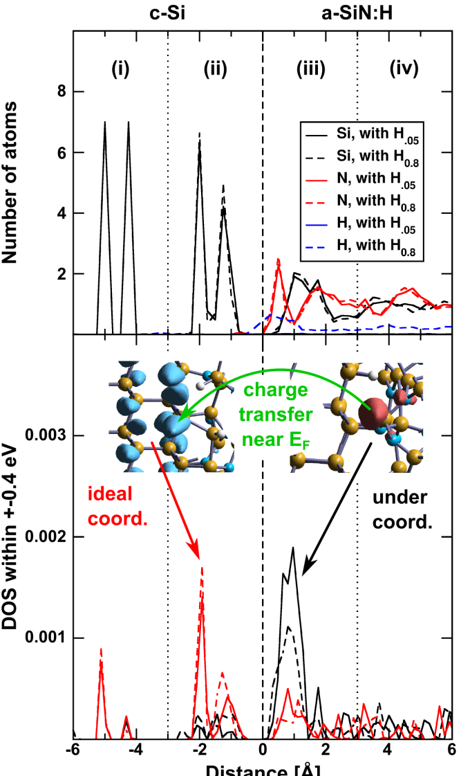
In the following, we summarize our most important results by investigating the layer resolved number densities and the electronic density of states (DOSs) at the c-Si/a-Si3N3.5:H interface (Fig. 1). The structural mismatch causes slight distortions in the first double layer of c-Si, and more important, long range density fluctuations in the a-SiN:H part, with a pronounced increase in the N density around Å (upper panel, red lines) above the Si topmost layer. These N atoms always bind to Si surface atoms, saturating % of the Si surface dangling bonds. The other Si surface atoms bind to Si atoms in the amorphous part. This causes the onset of a peak in the Si number density. The corresponding peak integrates to Si atoms per Si surface atom, and the region is unusually Si rich, with very little N content. Analysis of the bonding topology suggests that a large number of threefold coordinated Si K defects exists in this region, similar to, but in much greater number than in bulk a-SiN:H Hintzsche et al. (2013). These geometrical defects also cause a large number of electronic defect levels located in the band gap of c-Si [lower panel, region (iii)]. On the c-Si side, our analysis at first sight also suggests a large number of defects levels [lower panel, region (ii)], however, inspection of the charge density of these states indicates that these are conduction band like c-Si states (red arrow). We note that analysis of the large unit cell yields quantitatively identical results (not shown).
One central finding is that charge is partially transfered from originally occupied K defects in the a-SiN:H to the c-Si conduction band. This happens in % of our microscopic models (green arrow). This result, which is substantiated in detail below, explains the existence of the positive, fixed charge at c-Si/a-SiN:H interfaces. When H is present, the number density of H is clearly increased in the a-SiN:H part at the interface (upper panel, blue line), but the N and Si number densities are hardly changed. Although H reduces the number of K defects at the interface almost by a factor (lower panel, solid/dashed black line), our general observations remain unchanged.
III.2 Band structure and defect levels
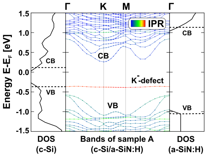
We now investigate three exemplary microscopic models in more detail. The first sample A contains a single localized doubly occupied K- defect in the middle of the gap (Fig. 3). In addition to the band structure of sample A, we show the DOSs of bulk undoped c-Si and a defect free bulk a-SiN:H model structure (left and right most panel). These bulk states have been aligned at the core levels of the Si and the N atoms in the middle of the c-Si and a-SiN:H part, respectively. The comparison of the bulk DOSs shows that the indirect band gap of c-Si (about eV) is much smaller than the band gap of a-SiN:H (about eV), and the conduction band offset (about eV) is larger than the valence band offset (about eV). That the band gaps are too small compared to experiment is a well known DFT artifact, however, as shown for instance in Ref. Flage˘Larsen et al., 2013, this error changes the mid gap levels, which are particularly relevant for this study, only very little. The present offsets are consistent with photo emission experiments and previous simulations on c-Si/c-Si3N4 interfaces Kärcher et al. (1984); Flage˘Larsen et al. (2013). The band structure furthermore demonstrates that the in plane dispersion of the defect level is negligible. This indicates that the lateral supercell size is generally sufficient, as there is no interaction between the periodically repeated defect images. However, the valence and the conduction band of c-Si show a strong dispersion necessitating a dense k-point sampling parallel to the interface.
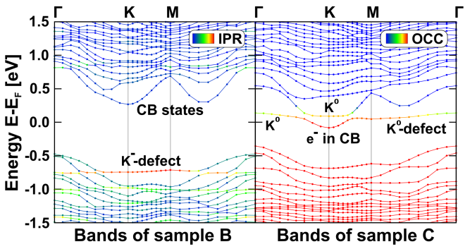
Since defect related states in the amorphous part can be situated anywhere within the gap of a-SiN:H Hintzsche et al. (2013), they often overlap with the c-Si conduction band or valence band. To give examples for such situations we show the band structure of two samples B and C (Fig. 3). In sample B, a doubly occupied K- defect merges into the c-Si valence band, and, in sample C, an initially doubly occupied K- defect merges into the c-Si conduction band. In both samples, the defect states are again strongly localized and practically flat. Nevertheless, since small hybridizations between the c-Si and the defect level exist, forbidden crossings are observed. The most interesting case is sample C. Here the average defect level is slightly above the conduction band minimum of c-Si, causing a partial transfer of charge from the defect level into the c-Si conduction band. This has reduced the occupancy (OCC) of the defect from K- to K0 and relates to the main finding mentioned above. The opposite, a partial transfer from the c-Si valence band to an originally empty K+ defect, is never observed.
III.3 Electronic states in the band gap
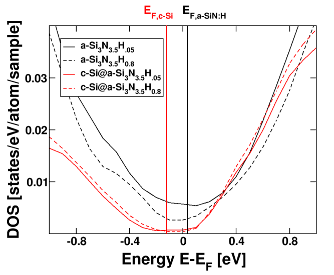
To obtain a statistically meaningful result, we now explore the electronic density of states evaluated close to the interface and averaged over all 90 samples (Fig. 4). On the c-Si side, we observe a slight band tailing introduced by local disorder and distorted Si bonds (red lines). However, the majority of the gap states are caused by undercoordinated Si atoms at the a-SiN:H side of the interface (black lines). The most important observation is that the minimum of the DOS of c-Si is shifted towards lower energy values (left) in comparison to the minimum of the DOS of a-SiN:H. Likewise, the mid gap energy level of bulk c-Si (red vertical line)— evaluated by taking the mean value of the valence band maximum and conduction band minimum of bulk Si — lies about eV below the average Fermi level of bulk a-SiN:H (black vertical line). Impaired by the issue of too small DFT band gaps, we believe that we observe only the lower bound of this offset here. Note that we have again taken the core levels of Si and N as reference for the alignment, and the general observations apply independently of the H concentration. As for our previous studies on bulk a-SiN:H Hintzsche et al. (2012, 2013), H mainly reduces the number of defects, although here it also slightly reduces the misalignment of the Fermi levels from eV to eV.
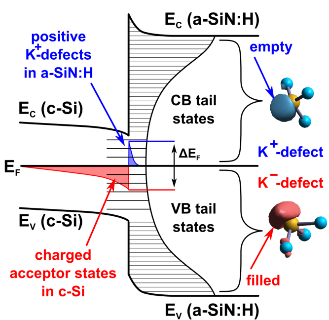
The offset of the mid gap level of Si and the Fermi level of a-SiN:H has important consequences. In a macroscopic sample, the Fermi levels must align and, in a real device, the alignment would occur via charge transfer from donors, here doubly occupied K- defects in a-SiN:H, to acceptor levels in c-Si as illustrated in Fig. 5. In our microscopic realizations this is not strictly so, since the Fermi level of the c-Si part can be located anywhere between the conduction and valence band: in the absence of acceptors and donors, the c-Si part does not pin the Fermi level mid gap. Only if an occupied K- defect is located above the conduction band of c-Si, a partial charge transfer to the c-Si part is observed, like in sample C. This partial charge transfer shifts the c-Si states upwards and the a-SiN:H states downwards. This line of thought indicates that it is not quite straightforward to determine highly accurate conduction band and valence band offsets between amorphous model structures and crystalline samples by using small model structures, even though we average over many microscopic models. That the mid gap level of c-Si lies well below the Fermi level of a-SiN:H is, however, a robust feature corroborated by three independent observations: (i) the observation of microscopic models with charge transfer to c-Si, (ii) the visual misalignment of the minima in the electronic DOSs, and (iii) the misalignment of the calculated c-Si mid gap level and the Fermi level of a-SiN:H.
IV Conclusions
In summary, we conclude that the number of undercoordinated Si atoms (K defects) is significantly increased at c-Si/a-SiN:H interfaces compared to bulk a-SiN:H (compare Fig. 1(b)). This is a result of the structural mismatch between c-Si and a-SiN:H. The number of coordination defects and related electronic defect states is reduced by about a factor in our simulations when H is present. Hence, hydrogen clearly cures geometrical defects at the interface, similar to bulk a-SiN:H. We predict a positive, fixed charge at c-Si/a-SiN interfaces related to a surplus of K+ defects on the a-SiN:H side screened by negatively charged acceptor states on the c-Si side (Fig. 5). In principle, this surplus is related to the mid gap level of bulk c-Si lying at least eV below the Fermi level of bulk a-SiN:H. Consequently, electrons must be transfered from originally doubly occupied K- defects on the a-SiN:H side, to acceptor levels on the c-Si side, to align the Fermi levels in the heterostructure. Solving the Poisson equation for this standard device problem results in a band bending at the interface (indicated by black lines in Fig. 5). Clearly such a band bending will attract electrons to the interface aiding the electron removal by metallic leads, which are etched into the a-SiN:H. Holes, on the other hand, are repelled making an effective separation of both carriers possible. Our present study also indicates that the number of K defects and the amount of positive charge at the interface are interrelated quantities. If the defect density is very low, there will be simply no defects that can donate charge to the c-Si part. This will reduce the positive interface charge and consequently the carrier separation. If the defect density is high, the fixed charge density will be high, but more recombination centers will be present as well. These results are exactly in line with recent experimental studies Lamers et al. (2012, 2014). Based on our present results, we suppose that it will be hard to achieve a negative, fixed charge by using the standard a-SiN:H passivation. The mid gap level of c-Si is well below the Fermi level of a-SiN:H, and only strong doping might change this. Moreover, it is impossible to reduce the density of carrier traps (K-, K0, and K+ defects) without changing the field effect passivation of fixed charges, as the species responsible for the fixed charges and K defects are identical.
Acknowledgement
This work is part of the HiperSol (high performance solar cells) project funded by the European commission grant no. MMP3-SL-2009-228513. Supercomputing time on the Vienna scientific cluster (VSC) is gratefully acknowledged.
References
- Luque and Hegedus (2011) A. Luque and S. Hegedus, Handbook of photovoltaic science and engineering (Wiley, 2011), ISBN 978-0470721698.
- Abou-Ras et al. (2011) D. Abou-Ras, T. Kichart, and U. Rau, Advanced characterization techniques for thin film solar cells (Wiley, 2011), ISBN 978-3527410033.
- Green et al. (2012) M. Green, K. Emery, Y. Hishikawa, W. Warta, and E. Dunlop, Progress in photovoltaics: research and applications 20, 12 (2012).
- Aberle (2000) A. G. Aberle, Progress in Photovoltaics: Research and Applications 8, 473 (2000).
- Duerinckx and Szlufcik (2002) F. Duerinckx and J. Szlufcik, Solar Energy Materials and Solar Cells 72, 231 (2002).
- Shockley and Read (1952) W. Shockley and W. Read, Phys. Rev. 87, 835 (1952).
- Hall (1952) R. Hall, Phys. Rev. 87, 387 (1952).
- Bube (1983) R. Bube, Fundamentals of solar cells: photovoltaic solar energy conversion (Academic Press, 1983), ISBN 978-0124142220.
- Green (1986) M. Green, Solar cells: operating principles, technology and system applications (University of New South Wales, 1986), ISBN 978-0858235809.
- Lamers et al. (2012) M. Lamers, K. Butler, J. Harding, and A. Weeber, Solar Energy Materials and Solar Cells 106, 17 (2012).
- Aberle (2001) A. Aberle, Sol. Energy Mater. Sol. Cells 65, 239 (2001), ISSN 0927-0248.
- Robertson et al. (1995) J. Robertson, W. Warren, and J. Kanicki, J. Non-Cryst. Solids 187, 297 (1995).
- Omeltchenko et al. (2000) A. Omeltchenko, M. Bachlechner, A. Nakano, R. Kalia, P. Vashishta, I. Ebbsjö, A. Madhukar, and P. Messina, Phys. Rev. Lett. 84, 318 (2000).
- Yang et al. (2009) M. Yang, R. Wu, W. Deng, L. Shen, Z. Sha, Y. Cai, Y. Feng, and S. Wang, Journal of Applied Physics 105, 024108 (2009).
- Butler et al. (2011) K. Butler, M. Lamers, A. Weeber, and J. Harding, J. Appl. Phys. 110, 124905 (2011).
- Butler et al. (2012) K. Butler, J. Harding, M. P. Lamers, and A. W. Weeber, Journal of Applied Physics 112, 094303 (2012).
- Flage˘Larsen et al. (2013) E. Flage˘Larsen, O. Løvvik, C. Fang, and G. Kresse, Phys. Rev. B 88, 165310 (2013).
- Lamers et al. (2013) M. Lamers, K. Butler, P. Vullum, J. Harding, and A. Weeber, Phys. Status Solidi (a) 210, 658 (2013).
- Lamers et al. (2014) M. Lamers, L. Hintzsche, K. Butler, P. Vullum, C. Fang, M. Marsman, G. Jordan, J. Harding, G. Kresse, and A. Weeber, Solar Energy Materials and Solar Cells 120, Part A, 311 (2014).
- Anh Pham et al. (2013) T. Anh Pham, T. Li, H.-V. Nguyen, S. Shankar, F. Gygi, and G. Galli, Applied Physics Letters 102, 241603 (2013).
- Hintzsche et al. (2012) L. Hintzsche, C. Fang, T. Watts, M. Marsman, G. Jordan, M. Lamers, A. Weeber, and G. Kresse, Phys. Rev. B 86, 235204 (2012).
- Blöchl (1994) P. Blöchl, Phys. Rev. B 50, 17953 (1994).
- Furthmüller et al. (1994) J. Furthmüller, J. Hafner, and G. Kresse, Phys. Rev. B 50, 15606 (1994).
- Kresse and Furthmüller (1996) G. Kresse and J. Furthmüller, Phys. Rev. B 54, 11169 (1996).
- Perdew et al. (2008) J. Perdew, A. Ruzsinszky, G. Csonka, O. Vydrov, G. Scuseria, L. Constantin, X. Zhou, and K. Burke, Phys. Rev. Lett. 100, 136406 (2008).
- Hintzsche et al. (2013) L. Hintzsche, C. Fang, M. Marsman, G. Jordan, M. Lamers, A. Weeber, and G. Kresse, Phys. Rev. B 88, 155204 (2013).
- Kärcher et al. (1984) R. Kärcher, L. Ley, and R. Johnson, Phys. Rev. B 30, 1896 (1984).