Addressing a single NV- spin with a macroscopic dielectric microwave cavity
Abstract
We present a technique for addressing single NV- center spins in diamond over macroscopic distances using a tunable dielectric microwave cavity. We demonstrate optically detected magnetic resonance (ODMR) for a single NV- center in a nanodiamond (ND) located directly under the macroscopic microwave cavity. By moving the cavity relative to the ND, we record the ODMR signal as a function of position, mapping out the distribution of the cavity magnetic field along one axis. In addition, we argue that our system could be used to determine the orientation of the NV- major axis in a straightforward manner.
Over the past decade, nitrogen-vacancy (NV) color centers in diamond (Figure 1(a)) have attracted a great deal of interest due to their outstanding quantum properties Doherty:PRep13 . Experiments have demonstrated long ground-state spin coherence times of the negatively charged NV center (NV-) even at room temperature Balasubramanian:NatMat09 . This makes NV- centers in diamond ideal candidates for room-temperature qubits Dutt:Science07 ; Neumann:Science08 and for ultrasensitive quantum sensors for detecting magnetic Balasubramanian:Nature08 ; Maze:Nature08 ; Degen:APL08 ; Taylor:NatPhys08 ; McGuinness:NatNano11 ; Grinolds:NatNano14 ; Tetienne:Science14 and electric fields Dolde:NatPhys11 at the nanoscale even in biological settings Faklaris:Small08 ; McGuinness:NatNano11 ; Ermakova:NanoLett13 .
Both quantum information processing and quantum sensing with NV- spins require the (coherent) manipulation and addressing of individual spins typically through the application of microwave (MW) radiation at a frequency that is resonant with the ground-state spin transition. The NV- exhibits a zero-field spin resonance at 2.87 GHz, which occurs between the and spin sublevels of its spin triplet ground state (see Figure 1b). The most commonly used approaches for applying microwaves at this frequency are on-chip microstrip lines (thin wires), coplanar waveguides, or free-space loop antennas. On-chip solutions rely on near-field coupling and require the NV- spin to be in close proximity (on the order of m) to the wire or microstrip line. Besides the inhomogeneity of the field, these on-chip solutions can easily lead to significant sample heating and undesired sample drift. Loop antennas typically work in the far field but require orders of magnitude larger amount of radiated MW power.

In order to address single NV- spins in diamond, we designed a so-called dielectric-loaded microwave resonator (DLR) with high quality (Q) factor (see Figure 1(c)). DLRs of this kind are typically used in low-temperature electron paramagnetic resonance experiments for measuring the complex permittivity of extremely low-loss dielectrics Tobar:JAP98 ; Krupka:MST99 ; LeFloch:PLA06 , but are also employed for testing local Lorentz invariance in fundamental experiments Tobar:PRD09 . In industrial settings, DLRs find applications in radar, proximity detection, information transmission, remote guiding, navigation and positioning Rieck:Proc08 ; Droz:Proc06 . In order to find an appropriate design for our DLR, we employed the numerical method of lines LeFloch:IEEE07 or finite element analysis. The design was guided by the desire to have compact cavity dimensions and the requirement for the field to couple evanescently to the NV- spins located in close vicinity under the cavity.
We found the best configuration to be an open cylindrically symmetric cavity with a pure transverse electric (TE) mode with two non-vanishing magnetic-field components, Hr and Hz. In contrast to whispering gallery modes, the TE-field confinement into the dielectric is not as high and exhibits less spurious modes, leading to a higher Q-factor LeFloch:RevSciInst14 . We denote the different cavity modes by TEm,n,p, where is the number of azimuthal nodes, the number of radial nodes, and the number of nodes along the z-axis (symmetry axis) of the cylinder. For pure TE-modes the azimuthal mode number vanishes, i.e. . Due to the particular boundary conditions, they only have three non-vanishing components of the electromagnetic field, and . By inserting a dielectric rod made of high-permittivity, low-loss microwave material, the field can be confined to an area of roughly mm2. From the few suitable materials available LeFloch:APL08 , we chose TiO2 for which the fundamental mode has a frequency of 2.2 GHz. For addressing the NV- spin transition, we then use the higher-order TE0,1,3-mode resonating at 2.7 GHz. Frequency tuning is achieved by mechanical insertion of a metallic plunger which directly affects the electric field and shifts the resonance frequency up to a value of 3.1 GHz (Figure 1(e)). The (loaded) Q-factor of this cavity mode is about 1,000 (see Figure 1(d)). Note that for perfect input coupling we would expect the circulating intra-cavity power to be enhanced by a factor Q compared to the incoming MW power. However, in the current cavity the coupling coefficient is rather small (about 1).
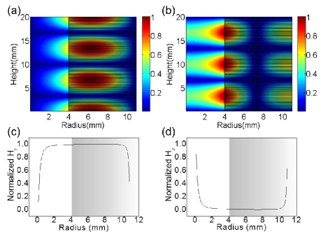
The magnetic field of the DLR cavity has cylindrical symmetry. Both the radial magnetic field strength, , and the vertical magnetic field strength, , are displayed in Figure 2. Figures 2 (a) and (b) show two-dimensional plots of the respective field strength in a plane that contains the symmetry axis of the cavity: The x-axis corresponds to the radial distance from the symmetry axis and the values on the y-axis indicate the height above the bottom edge of the cavity. We note that the radial field component has a maximum right at the bottom edge at mm, indicating a strong evanescent component. The vertical field is well-contained within the cavity. Figure 2 (c) and (d) show the expected variation of the radial and vertical field in a plane mm below the cavity. The plots are normalized to the local overall field strength . The graphs clearly show that in the center of the cavity the component dominates (due to symmetry) whereas right under the dielectric at mm, the radial field is the dominant component.
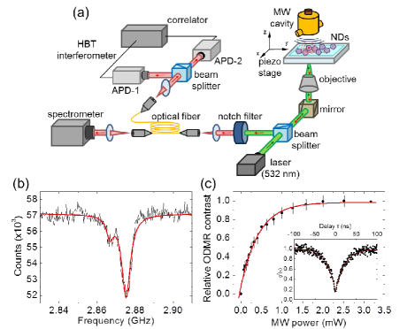
We now move on to demonstrate ODMR of a single NV- spin located just below the cavity. The HPHT nanodiamonds (MSY 0.1 m, Microdiamant) are placed on a glass coverslip approximately 1 mm below the cavity which is mounted on a x-y-z mechanical stage (see Figure 3(a)). The ND fluorescence upon excitation with a 532 nm laser is collected using a home-built confocal microscope Bradac:NatNano10 and sent to either a spectrometer or to avalanche photodetectors. Once a suitable single NV- center is identified, we obtain an ODMR signal by applying microwave radiation through our microwave cavity and recording the corresponding fluorescence as a function of microwave frequency. The microwave signal is generated using a standard microwave generator (SMIQ 06B, Rohde Schwarz) and amplified (25S1G4A, Amplifier Research) before applying it to the cavity. A typical ODMR signal is displayed in Figure 3(b), clearly demonstrating the coupling of a single NV- spin to the macroscopic microwave resonator. Note that the contrast of the ODMR signal was optimized by adjusting the cavity resonance frequency to the actual transition frequency of the selected NV- center. Depending on the ND, we found a maximum achievable contrast of up to . Next, we recorded a saturation curve for the transition 3(c) giving a saturation power of about 5 dBm for this particular NV- spin.
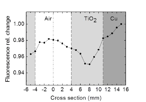
In order to demonstrate the spatial variation of the magnetic field, we recorded an ODMR signal as a function of relative position between the ND and the center axis of the cavity by mechanically adjusting the cavity position. In the low-power (or linear) regime, the contrast of the ODMR signal measures the local microwave power seen by the NV- spin. Figure 4 shows the result of such a measurement taken along the x-axis in consecutive 1-mm steps, while the z- and y-coordinates of the resonator were kept fixed with respect to the ND position. In the figure, we plot the depth of the ODMR resonance as a function of position, normalized to 1. The plot displays the expected variation in ODMR contrast and exhibits a maximum contrast of about 6 when the ND is right below the dielectric of the cavity structure at mm. The finite contrast at indicates that the NV- spin has a non-vanishing in-plane component. Since we do not know the major axis of the NV- center, we cannot extract the full information about the cavity magnetic field from Figure 4. Using a ND with a known spin orientation, however, magnetic-field tomography is possible. The cavity presented here could also be used as a tool to determine the major axis of a single NV- center in a straightforward manner: By measuring the ODMR contrast in the center of the cavity and in two additional points along the circumference just below the dielectric slab at mm, the direction of the NV- spin can be calculated - provided the ratio is known.
The main advantages of our new technique are the large area over which the spins can be addressed and the absence of undesired sample heating allowing for stable long-term observations. Our measurements once again demonstrate the potential of NV- centers as robust technologically viable magnetic-field sensors. In addition, the DLR cavity can serve as a tool for identifying the orientation of NV- spins. In the future, we plan to use the device for coherent time-resolved spin manipulation.
References
- (1) M. W. Doherty,N. B. Manson, P. Delaney, F. Jelezko, J. Wrachtrup, and L. C. L. Hollenberg, Physics Reports 528, 1 (2013).
- (2) G. Balasubramanian et al., Nature Materials, 8, 383-387 (2009).
- (3) M. V. Gurudev Dutt1, L. Childress, L. Jiang, E. Togan, J. Maze, F. Jelezko, A. S. Zibrov, P. R. Hemmer, and M. D. Lukin Science, 316, 1312-1316 (2007).
- (4) P. Neumann, N. Mizuochi, F. Rempp, P. Hemmer, H. Watanabe, S. Yamasaki, V. Jacques, T. Gaebel, F. Jelezko, and J. Wrachtrup Science 320, 1326-1329 (2008).
- (5) G. Balasubramanian et al., Nature 455, 648-651 (2008).
- (6) J. R. Maze et al., Nature, 455, 644-647 (2008).
- (7) C.L. Degen Applied Physics Letters, 92, 243111 (2008).
- (8) J. M. Taylor, P. Cappellaro, L. Childress, L. Jiang, D. Budker, P. R. Hemmer, A. Yacoby, R. Walsworth, and M. D. Lukin Nature Physics 4, 810-816 (2008).
- (9) L.P. McGuinness et al., Nature Nanotechnology 6, 358-363 (2011).
- (10) M. S. Grinolds, M. Warner, K. De Greve, Y. Dovzhenko, L. Thiel, R. L. Walsworth, S. Hong, P. Maletinsky, and A. Yacoby Nature Nanotechnology 9, 279-284 (2014).
- (11) J.-P. Tetienne et al., Science 344, 1366-1369 (2014).
- (12) F. Dolde et al., Nature Physics, 7, 459-463 (2011).
- (13) O. Faklaris, D. Garrot, V. Joshi, F. Druon, J. P. Boudou, T. Sauvage,. P. Georges, P. A. Curmi, and F. Treussart, Small 4, 2236 (2008).
- (14) A. Ermakova et al., Nano Letters 13, 3305-3309 (2013).
- (15) M.E. Tobar, J. Krupka, E.N. Ivanov, and R.A. Woode Journal of Applied Physics 83, 1604 (1998).
- (16) J. Krupka, K. Derzakowski, M.E. Tobar, J. Hartnett, and R.G. Geyerk, Measurement Science and Technology 10, 387-392 (1999).
- (17) J.-M. Le Floch et al., Physics Letters A 359, 1-7 (2006).
- (18) M.E. Tobar, E.N. Ivanov, P.L. Stanwix, J.-M. Le Floch, and J.G. Hartnett, Physical Review D 80, 125024 (2009).
- (19) C. Rieck, P. Jarlemark, R. Emardson, and K. Jaldehag, Proc. 22nd EFTF, Toulouse, France, 2008.
- (20) F. Droz, P. Mosset, G. Barmaverain, P. Rochat, Q. Wang, M. Belloni, L. Mattioni, F. Emma, and P. Waller, Proc. 20th EFTF, Braunschweig, Germany, 2006.
- (21) J.-M. Le Floch, M.E. Tobar, D. Cros, and J. Krupka, IEEE Trans. Ultrason. Ferroelec. Freq. Contr. 54, 2689-1695 (2007).
- (22) J.-M. Le Floch et al., Review of Scientific Instruments 85, 031301 (2014).
- (23) J.-M. Le Floch, M.E. Tobar, D. Cros, and J. Krupka, Applied Physics Letters,92, 032901 (2008).
- (24) C. Bradac et al., Nature Nanotechnology 5, 345-349 (2010).