Domain wall magneto-Seebeck effect
Abstract
The interplay between charge, spin, and heat currents in magnetic nano systems subjected to a temperature gradient has lead to a variety of novel effects and promising applications studied in the fast-growing field of spincaloritronics. Here we explore the magnetothermoelectrical properties of an individual magnetic domain wall in a permalloy nanowire. In thermal gradients of the order of few along the long wire axis, we find a clear magneto-Seebeck signature due to the presence of a single domain wall. The observed domain wall magneto-Seebeck effect can be explained by the magnetization-dependent Seebeck coefficient of permalloy in combination with the local spin configuration of the domain wall.
Electronic transport coefficients in ferromagnetic materials are spin-dependent Mott and Jones (1953) enabling important spintronics applications Zutic et al. (2004). This observation also holds for magnetothermoelectric (or spincaloritronic) phenomena Johnson and Silsbee (1987); Bauer et al. (2010a, 2012), driven by thermal gradients Uchida (2008); Slachter et al. (2010); LeBreton et al. (2011); Jeon et al. (2014). In a thermal gradient, the temperature difference between two contacts gives rise to a thermopower with being the material’s Seebeck coefficient. Spin-dependent Seebeck coefficients have been observed in various nanomagnetic systems like thin films Avery et al. (2012); Schmid et al. (2013), multilayers Shi et al. (1993), tunnel junctions Czerner et al. (2011); Walter et al. (2011); Liebing et al. (2011), and nanowires Böhnert et al. (2013); Gravier et al. (2006). In the latter, magnetization reversal often occurs by the nucleation and propagation of a single magnetic domain wall (DW) enabling promising applications Ono et al. (1999); Allwood et al. (2005); Parkin et al. (2008). Also a DW can interact with a thermal gradient Berger (1985); Hatami et al. (2007); Kovalev and Tserkovnyak (2009) with prospects for thermally driven DW motion Hinzke and Nowak (2011); Yan et al. (2011); Torrejon et al. (2013); Jiang et al. (2013) or nanoscale magnetic heat engines Bauer et al. (2010b). However, the fundamental thermoelectrical properties of an individual magnetic DW have not been investigated yet.
In our experiments we use L-shaped permalloy (Py) nanowires with a notch (see Fig. 1A and supplementary material for details). The L’s corner allows a controlled nucleation of a DW while the notch allows pinning a moving DW between the electrical probes. The two probes are contacting the Py wire from the top for resistance and thermopower measurements. Two additional Pt strips located at a distance of and from the Py nanowire serve as resistive thermometer and heater, respectively. The magnetic behavior of the system is characterized by two-wire resistance measurements as a function of magnetic field at a DC current of . In a first step, the magnetization of the entire wire is rotated from the longitudinal () to the transversal () direction by a magnetic field applied at , i.e. along the -direction (note the definition of coordinates in Fig. 1A). As expected for a system dominated by the anisotropic magnetoresistance (AMR), the measurement shows a bell-shaped curve (Fig. 2A) with resistance being decreased by the field of either polarity by . We find at remanence and at maximum transversal field and hence a two-wire AMR ratio . In a second step, we study the AMR contribution of a single DW. For this purpose we apply a field in diagonal direction () to create a head-to-head DW at the corner which is than moved towards the notch by a field applied at any . As an example, Fig. 2B shows a measurement at . The DW arrives at the notch at , where it remains until is reached. The presence of the DW at the notch leads to a decrease of resistance by approximately . The resistance drop is due to transversally oriented magnetization within the DW and based entirely on AMR. The critical fields and are the pinning fields of the corner and of the notch, respectively. To fully characterize the DW dynamics we repeat the measurement in the angle-range . The results are presented in Fig. 1C, where the resistance is indicated by a color-scale. The yellow region indicates the resistance lowered due to the presence of the DW at the notch. Typically the left edge of this region is smooth whereas the right edge is rather irregular. This means that the pinning strength of the corner for various angles is well defined Corte-Leon et al. (2014) whereas the pinning strength of the notch has a stronger stochastic component. We model the magnetization distribution during field-driven DW motion by micromagnetic simulations using a Landau-Lifshitz-Gilbert micromagnetic simulator Scheinfein et al. (1991). Our numerical analysis predicts that a vortex-type of DW is nucleated at the corner as pictured in Fig. 3D, where a snapshot of the magnetization distribution at during a field sweep at is shown. For increasing field strength, the vortex DW will be ’pulled’ deeper into the notch, deformed and finally transformed into a transversal DW before depinning, which explains the stochastic behavior of .
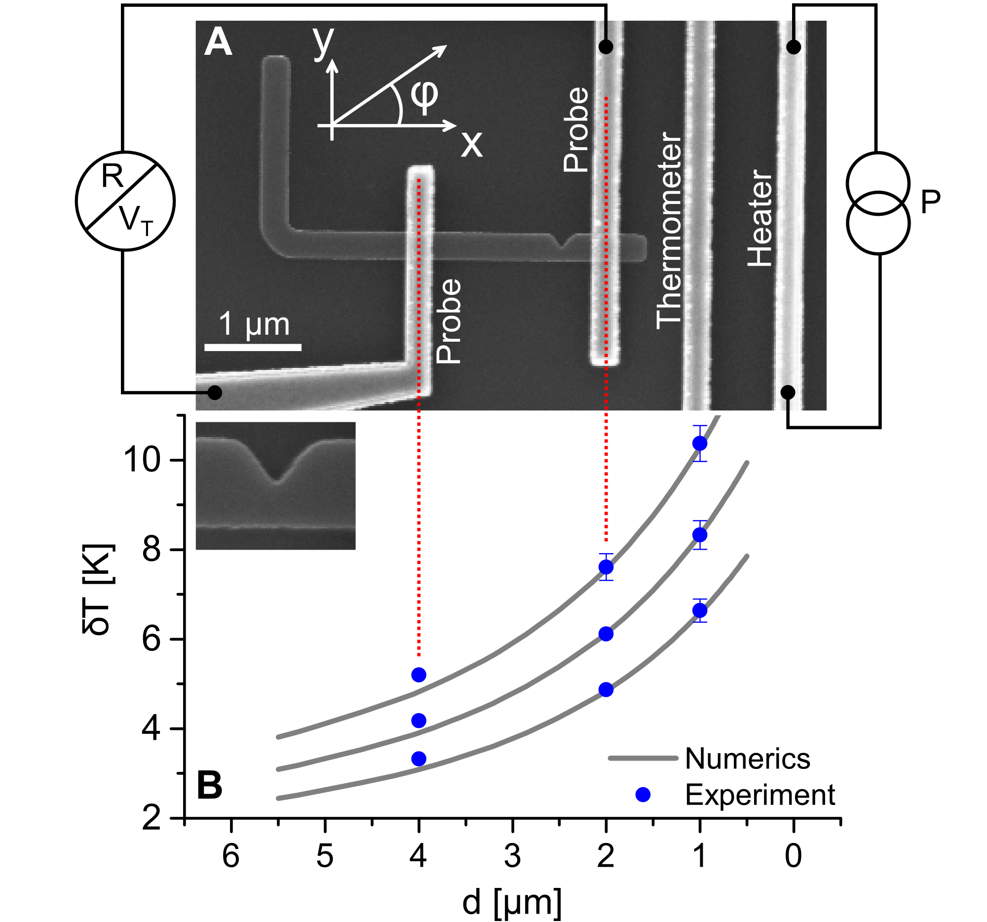
For thermoelectrical measurements, we generate temperature gradients by applying an AC power at a frequency of to the heater. To characterize the temperature distribution we use calibration samples with identical heaters and thermometers placed correspondingly to the positions of the voltage probes (red lines in Fig. 1A). For each heater power , the thermometer resistance has a AC component with amplitude detected by 4-wire lock-in measurements. To translate to the temperature increase we first determine the temperature coefficient in a separate setup. We find which is 30 % of the bulk value in good agreement with literature Zhang et al. (2005). Figure 1B shows the measured (blue bullets) as a function of the distance from the heater for three heating powers: , and . The temperature distribution is further investigated by three-dimensional finite-element modeling. The numerical results (gray lines) show a good agreement with the experimental data. Heating with accordingly leads to an increase of the nanowire temperature of up to and a between the probes of . In the following, the thermopower is measured at by lock-in detection at via the voltage probes.
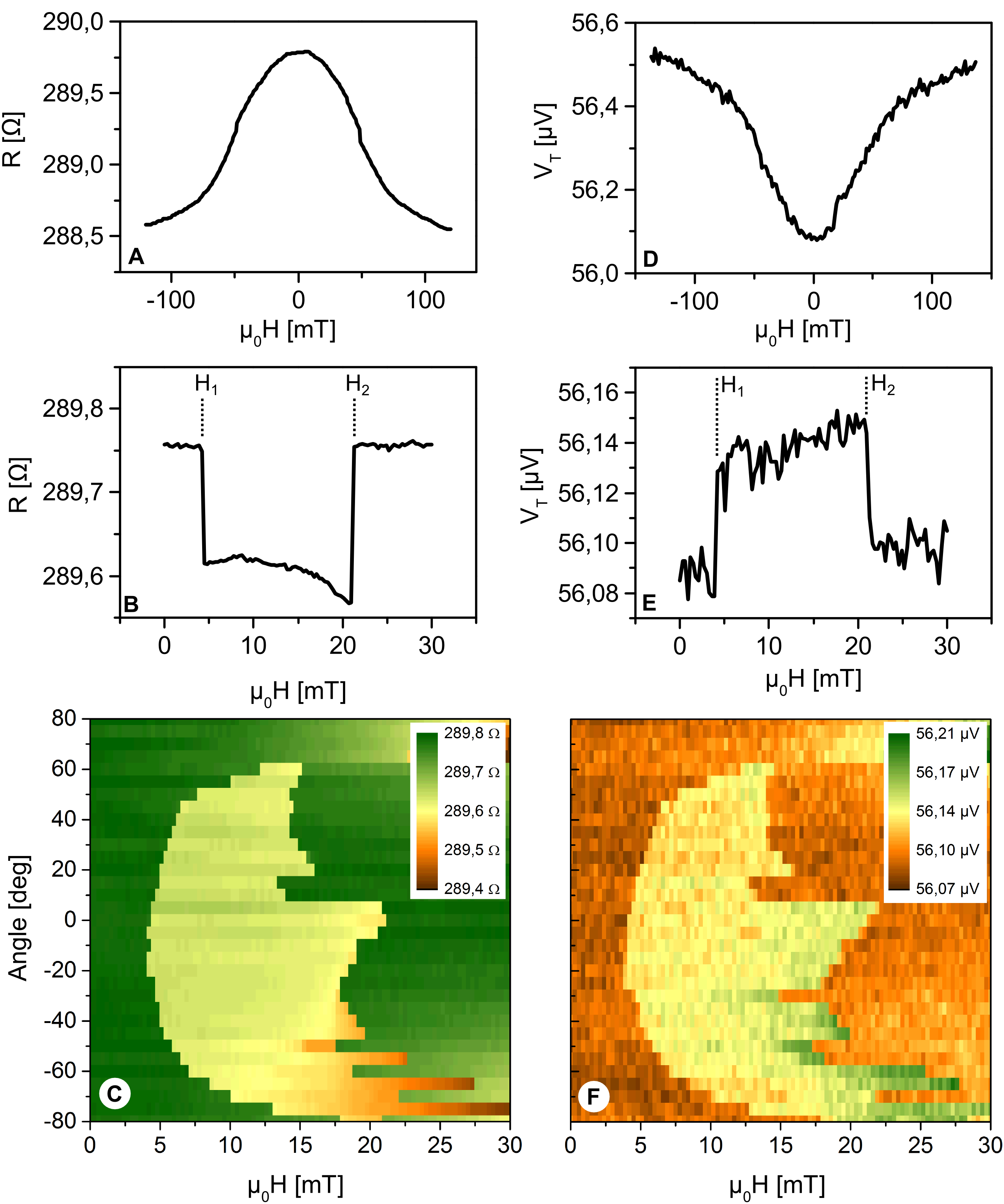
Figure 2D shows the evolution of the thermopower as a function of transversal field (, cf. Fig. 2A). Again, a bell-shaped curve comes into view, but with the thermopower being increased by a magnetic field of either polarity. We find a thermopower of at remanence and at maximum field with an accuracy of . The effective Seebeck coefficient is . The magnetothermopower (MTP) ratio yields . The Seebeck coefficient of the nanowire thus rises when the wire’s magnetization rotates under the action of an external field. For comparison of magnetoresistance (MR) and magento-Seebeck ratio the lead contributions have to be taken into account as discussed in the supplementary material. In the following we investigate the change of thermopower induced by the presence of a single DW. As an example, Fig. 2E shows a MTP measurement at the same conditions as the MR measurement shown in Fig. 2B. As the field reaches , we observe a sudden increase of thermopower by approx. . The thermopower remains roughly constant at this level until the field reaches , where it drops back to the base level. Figure 2F shows the complete set of DW thermopower (DWTP) measurements for angles . In this color plot, the yellow area indicates the increased thermopower. If we compare the pinning fields from MR and thermopower measurements (Figs. 2C and 2F), and keep the stochastic nature of in mind, we can safely consider them as identical. Evidently the origin of increased thermopower is the same as the origin of reduced resistance, namely the presence of a DW at the notch. The data thus clearly reveal the thermoelectrical signature of a single DW.
To analyze our data, we describe the thermopower of a system magnetized along the -direction by
| (1) |
where the Seebeck coefficient has tensor character analogous to the resistivity tensor (see supplementary material). The diagonal elements of the tensor represent the anisotropy of the Seebeck coefficient; is measured when the temperature gradient is parallel to the magnetization direction while is measured when it is transversal to the magnetization direction (cf. Fig. 2d). We consider also the anomalous Nernst effect (ANE) by the off-diagonal elements , which will generate an additional thermopower in the case of a non-vanishing out-of-plane temperature gradient Slachter et al. (2011). Our experimental setup is designed to detect the thermopower generated along the wire direction thus we consider only the -component of Eq. 3. The resulting MTP can be described by three terms
| (2) | |||||
where is the angle of the local magnetization direction with respect to the -direction (see supplementary material). Due to the analogy with AMR, we refer to the first term as anisotropic magneto-Seebeck (AMS) effect. The second term is related to the planar Nernst effect (PNE) Avery et al. (2012) and the third term describes the ANE contribution of an in-plane magnetized system. We use our numerical results of magnetization distribution and temperature gradients to verify this approach. The nanowire is divided in cells of . For each cell we take the local magnetization direction and the temperature difference across the cell to calculate the local thermopower according to Eq. 2. To estimate the global thermopower, we calculate the mean thermopower generated in each 10-nm-slice of the wire and sum over all slices between the voltage probes. We repeat those calculations for various magnetic configurations (cf. Fig. 3D) corresponding to the movement of a DW during a field-sweep at . The temperature gradients are shown as a color map in Fig. 3E–G (note the different color scales for in-plane and out-of-plane directions).
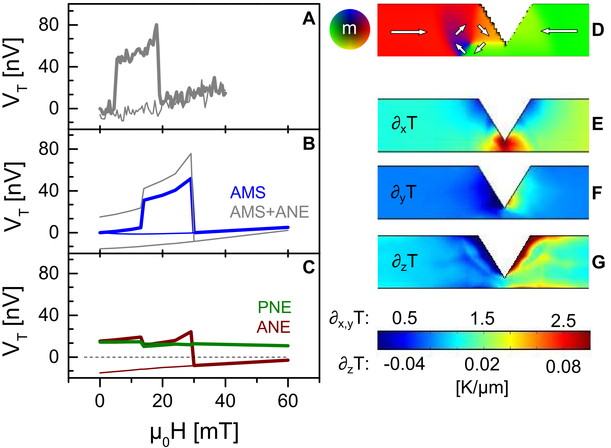
Figure 3A shows the measured DWTP for with the thermopower of the remanent state set to zero. The calculation considering only the AMS is shown in Fig. 3B by the blue curve. Considering the typical deviations of a micromagnetic model a very good agreement between experiment and simulation is obtained. Our analysis thus reveals that the DWTP is dominated by the AMS (first term in Eq. 2) and the remaining terms of Eq. 2 are treated as corrections. The expected PNE contribution is indicated by the green line in Fig. 3C. It shows a nearly constant value of approx. with a DW signature of only . Within the experimental noise level, PNE should hence have no impact on the DWTP. Figure 3C also plots the ANE contribution (brown line). At the ANE has a value of about . During the DW pinning only a small change of the ANE signal occurs. However, at the ANE signal shows a sudden drop and a change of sign. Here the magnetization direction at the hot side of the notch is reversed due to the depinning of the DW. In the following up-sweep to and the back-sweep to a linear behavior is found. ANE should thus lead to a splitting of the signal at zero field. Taking into account both, AMS and ANE, leads to the grey curve in Fig. 3B. Clearly, this splitting predicted at low fields is not observed in the experiment. From that we can conclude that the ANE is not significant in the experimental data and seems to be overestimated by the model. Note that the temperature model is based on a wire with sharp rectangular cross sections and a sharp V-shaped notch. This leads to an overestimation of the out-of-plane gradients at the notch and hence of the ANE contribution compared to the real device with rounded edges and smooth notch (cf. Fig. 1B, inset).
Similar results have been obtained on various devices with varying geometries confirming that a slight variation of the nanowire width or the notch shape does not change the general behavior. Furthermore, no significant difference between head-to head and tail-to-tail DWs was found. Our data thus clearly reveal the thermopower contribution of an individual DW in a magnetic nanowire thereby providing the fundamental link between macroscopic thermoelectrical signature and nanomagnetic spin configuration.
References
- Mott and Jones (1953) N. F. Mott and H. Jones, Theory of the properties of metal and alloys (Oxford University Press, 1953).
- Zutic et al. (2004) I. Zutic, J. Fabian, and S. D. Sarma, Rev. Mod. Phys. 76 (2004).
- Johnson and Silsbee (1987) M. Johnson and R. H. Silsbee, Phys. Rev. B 35, 4959 (1987).
- Bauer et al. (2010a) G. E. W. Bauer, A. H. MacDonald, and S. Maekawa, Solid State Commun. 150, 459 (2010a).
- Bauer et al. (2012) G. E. W. Bauer, E. Saitoh, and B. J. van Wees, Nature Materials 11, 391 (2012).
- Uchida (2008) K. Uchida, Nature 455, 778 (2008).
- Slachter et al. (2010) A. Slachter, F. L. Bakker, J. P. Adam, and B. J. van Wees, Nature Phys. 6, 879 (2010).
- LeBreton et al. (2011) J.-C. LeBreton, S. Sharma, H. Saito, S. Yuasa, and R. Jansen, Nature 475, 82 (2011).
- Jeon et al. (2014) K.-R. Jeon, B.-C. Min, A. Spiesser, H. Saito, S.-C. Shin, S. Yuasa, and R. Jansen, Nature Materials 13, 360 (2014).
- Avery et al. (2012) A. D. Avery, M. R. Pufall, and B. L. Zink, Phys. Rev. Lett. 109, 196602 (2012).
- Schmid et al. (2013) M. Schmid, S. Srichandan, D. Meier, T. Kuschel, J.-M. Schmalhorst, M. Vogel, G. Reiss, C. Strunk, and C. H. Back, Phys. Rev. Lett. 111, 187201 (2013).
- Shi et al. (1993) J. Shi, R. C. Yu, S. S. P. Parkin, and M. B. Salamon, J. Appl. Phys. 73, 5524 (1993).
- Czerner et al. (2011) M. Czerner, M. Bachmann, and C. Heiliger, Phys. Rev. B 83, 132405 (2011).
- Walter et al. (2011) M. Walter, J. Walowski, V. Zbarsky, M. Muenzenberg, M. Schaefers, D. Ebke, G. Reiss, A. Thomas, P. Peretzki, M. Seibt, et al., Nature Materials 10, 742 (2011).
- Liebing et al. (2011) N. Liebing, S. Serrano-Guisan, K. Rott, G. Reiss, J. Langer, B. Ocker, and H. W. Schumacher, Phys. Rev. Lett. 107, 177201 (2011).
- Böhnert et al. (2013) T. Böhnert, V. Vega, A.-K. Michel, V. M. Prida, and K. Nielsch, Appl. Phys. Lett. 103, 092407 (2013).
- Gravier et al. (2006) L. Gravier, S. Serrano-Guisan, F. Reuse, and J. P. Ansermet, Phys. Rev. B 73, 024419 (2006).
- Ono et al. (1999) T. Ono, H. Miyajima, K. Shigeto, K. Mibu, N. Hosoito, and T. Shinjo, Science 284, 486 (1999).
- Allwood et al. (2005) D. A. Allwood, G. Xiong, C. C. Faulkner, D. Atkinson, D. Petit, and R. P. Cowburn, Science 309, 1688 (2005).
- Parkin et al. (2008) S. S. P. Parkin, M. Hayashi, and L. Thomas, Science 320, 190 (2008).
- Berger (1985) L. Berger, J. Appl. Phys. 58, 450 (1985).
- Hatami et al. (2007) M. Hatami, G. E. W. Bauer, Q. Zhang, and P. J. Kelly, Phys. Rev. Lett. 99, 066603 (2007).
- Kovalev and Tserkovnyak (2009) A. Kovalev and Y. Tserkovnyak, Phys. Rev. B 80, 100408R (2009).
- Hinzke and Nowak (2011) D. Hinzke and U. Nowak, Phys. Rev. Lett. 107, 027205 (2011).
- Yan et al. (2011) P. Yan, X. S. Wang, and X. R. Wang, Phys. Rev. Lett. 107, 177207 (2011).
- Torrejon et al. (2013) J. Torrejon, G. Malinowski, M. Pelloux, R. Weil, A. Thiaville, J. Curiale, D. Lacour, F. Montaigne, and M. Hehn, Phys. Rev. Lett. 110, 177202 (2013).
- Jiang et al. (2013) W. Jiang, P. Upadhyaya, Y. Fan, J. Zhao, M. Wang, L.-T. Chang, M. Lang, K. L. Wong, M. Lewis, Y.-T. Lin, et al., Phys. Rev. Lett. 110, 177202 (2013).
- Bauer et al. (2010b) G. E. W. Bauer, S. Bretzel, A. Brataas, and Y. Tserkovnyak, Phys. Rev. B 81, 024427 (2010b).
- Corte-Leon et al. (2014) H. Corte-Leon, V. Nabaei, A. Manzin, J. Fletcher, P. Krzysteczko, H. W. Schumacher, and O. Kazakova, Sci. Rep. 4, 6045 (2014).
- Scheinfein et al. (1991) M. R. Scheinfein, J. Unguris, J. L. Blue, K. J. Coakley, D. Pierce, R. J. Celotta, and P. Ryan, Phys. Rev. B 43, 3395 (1991).
- Zhang et al. (2005) X. Zhang, H. Xie, M. Fujii, H. Ago, K. Takahashi, T. Ikuta, H. Abe, and T. Shimizu, Appl. Phys. Lett. 86, 171912 (2005).
- Slachter et al. (2011) A. Slachter, F. L. Bakker, and B. J. van Wees, Phys. Rev. B 84, 020412 (2011).
- Soni and Okram (2008) A. Soni and G. S. Okram, Rev. Sci. Inst 79, 125103 (2008).
- Ho et al. (1978) C. Y. Ho, M. W. Ackerman, K. Y. Wu, S. G. Oh, and T. N. Havill, J. Phys. Chem. Ref. Data 7, 959 (1978).
- Owen et al. (1937) E. A. Owen, E. L. Yates, and A. H. Sully, Proc. Phys. Soc. 49, 315 (1937).
- Bonnenberg et al. (2000) D. Bonnenberg, K. A. Hempel, and H. P. J. Wijn, Springer Materials: The Landolt-Brönstein Database (Springer, 2000).
- Hankenmeier et al. (2008) S. Hankenmeier, K. Sachse, Y. Stark, R. Frömter, and H. Oepen, Appl. Phys. Lett. 92, 242503 (2008).
- Banhart and Ebert (1995) J. Banhart and H. Ebert, Europhys. Lett. 32, 517 (1995).
Supplementary material
.1 Device Fabrication
In our experiments we use an L-shaped Py nanowire with a notch. The nanowire is wide and has arms of and length. The longer arm has a notch, deep and wide, at a distance of from the corner. The nanostructure is patterned by electron beam lithography in combination with Ar ion etching from a continuous Py film that has been sputter-deposited on a Si substrate covered by a SiO layer. The Py is thick and covered with a Pt cap of to prevent oxidation. Additionally, devices without Pt cap were fabricated to ensure that the Pt capping layer has no significant influence on the DWTP. In a second lithography step, we attach Pt wires as voltage probes. The Pt wires are thick with a Ta adhesion layer. The interface between Py and Ta is cleaned in-situ by low energy Ar ions prior to Ta/Pt deposition to ensure good electrical contact. Two additional Pt strips located at a distance of and from the Py nanowire serve as resistive thermometer and heater, respectively.
.2 Temperature calibration
To detect the temperature gradient experimentally, at least two thermometers are needed, each sensitive to the temperature at a certain distance from the heat source. We fabricate a set of nominally identical devices with heater-thermometer pairs separated by . For each distance, the calibration is repeated for four different devices to increase the statistical significance. The temperature coefficient of the Pt thermometer is measured by 4-wire resistance measurements as a function of the temperature of a hot plate heated to up to above room temperature. We use thermal grease and an equilibration time of at least to ensure uniform temperature distribution before taking a value. The resulting temperature coefficient allows for a measurement of the local temperature increase with an accuracy of approx. . This results in an uncertainty of the temperature difference measured between and of approx. . This uncertainty is not to be confused with poor time-stability.
.3 The influence of the wiring
The 2-wire AMR ratio is . This value, however, is obscured by the resistance of the wiring which is estimated on the basis of 4-wire measurements on similar devices to . This yields a 4-wire AMR ratio of .
Also the measured Seebeck coefficients are influenced by the electrical contacts. Considering a temperature gradient with , the nominal Seebeck coefficient of the permalloy-platinum thermocouple is and for the longitudinal and transversal geometry, respectively. This yields a magneto-Seebeck ratio of . The Pt voltage probe contributes its own thermopower of due to a Seebeck coefficient of Soni and Okram (2008). The resulting absolute Seebeck coefficients of permalloy are and with an uncertainty of . This yields an absolute magneto-Seebeck ratio of .
.4 Modeling
For micromagnetic simulations we use a commercial micromagnetic modeling tool (llg Micromagnetics Simulator) Scheinfein et al. (1991) with the following parameters: saturation magnetization , exchange stiffness , and uniaxial anisotropy constant oriented along the long wire. The cells size is . The simulation temperature is zero Kelvin.
| Parameter | Permalloy | SiO | Si |
|---|---|---|---|
| Thermal conductivity [] | 46.4 Ho et al. (1978) | 1.4 | 130 |
| Density [] | 8700 Owen et al. (1937) | 2200 | 2329 |
| Heat capacity [] | 430 Bonnenberg et al. (2000) | 730 | 700 |
| Electrical conductivity [] | Hankenmeier et al. (2008) | 0 |
The temperature distribution is modeled by a commercial finite-element modeling tool (comsol Multiphysics). The input parameters are displayed in Tab. 1. The boundary condition ‘convective cooling’ is activated for all surfaces in contact with air. The temperature of the air and of the bottom surface of the SiO substrate is fixed at .
.5 The Seebeck tensor
An n-type conductor placed in a temperature gradient generally accumulates negative charge at the cool side leading to an electrical field pointing away from the heat source. The efficiency of this process is described by the Seebeck coefficient with (by this definition the Seebeck coefficient is negative for n-type conductors). It is customary to use and rewrite this equation to which by integration directly leads to the measured voltage . This voltage, which is referred to as thermopower, is generated between two points with a temperature difference of .
Our phenomenological description of the magneto-Seebeck effect is based on the according description of the magnetoresistance Banhart and Ebert (1995). The Seebeck tensor for systems with the magnetization along the -direction has the form
| (3) |
where is a measure of the anomalous Nernst effect. and are the longitudinal and transversal Seebeck coefficients, respectively. For a magnetization vector pointing in an arbitrary direction in the -plane we need to transform the Seebeck tensor using the rotational matrix with the angle of the magnetization in respect to the -axis
| (4) |
Using this result can be written as
| (5) |
In our devices we are sensitive to the -component of this vector which yields
| (6) |
We use the experimental results and as well as taken from literature Slachter et al. (2011).