Topological defect lasers
Abstract
We demonstrate topological defect lasers in a GaAs membrane with embedded InAs quantum dots. By introducing a disclination to a square-lattice of elliptical air holes, we obtain spatially confined optical resonances with high quality factor. Such resonances support powerflow vortices, and lase upon optical excitation of quantum dots, embedded in the structure. The spatially inhomogeneous variation of the unit cell orientation adds another dimension to the control of a lasing mode, enabling the manipulation of its field pattern and energy flow landscape.
pacs:
PACS numbers: 75.60.Ej, 64.60.AkTopological defects have been extensively studied in nematic liquid crystals and colloids. Senyuk et al. (2013); Muševič (2013); Loussert et al. (2013); Brasselet and Loussert (2011); Brasselet (2010); Barboza et al. (2012, 2013). There are various types of nematic defects that are characterized by a distinct orientational alignment of rod-shaped molecules or colloidal particles, creating a discontinuity in the director field around a fixed point. One important application of topological defects to photonics is the generation of optical beams with orbital angular momenta Brasselet et al. (2009); Barboza et al. (2012, 2013). Also tightly focused laser beams have been used to manipulate topological defects in liquid crystals Smalyukh et al. (2007); Brasselet et al. (2008, 2009). All these studies have been carried out on passive systems. It is not known what will happen when optical gain is introduced to the topological defect structure, whether it is possible to achieve lasing, and if so, what the lasing characteristic will be. The study, presented in this paper, aimed to answer these questions.
In order to realize lasing in the topological defect structure, optical confinement must be strong to enhance light amplification. Due to the small size of liquid crystal molecules (nm) and low refractive index modulation, light cannot be effectively confined in naturally occurring topological defects. To improve optical confinement, we introduce topological defects to photonic crystals (PhCs). In a PhC, periodic modulation of refractive index on the length scale of optical wavelength can produce a photonic bandgap (PBG) within which light cannot propagate Soukoulis (2001); Noda and Baba (2003); Sakoda (2005); Joannopoulos et al. (2011). Creation of a structural defect in the PhC then produces localized states inside the PBG that typically have high quality () factor. Painter et al. (1999a, b); Park et al. (2001); Ryu et al. (2002). By introducing the spatial variation of the unit cell orientation, we add another degree of control of the lasing mode characteristic.
In this Letter, we present the design, fabrication and characterization of a topological defect laser. A square lattice of ellipse-shaped air holes are etched in a GaAs membrane. The air hole size as well as the lattice constant is on the order of the optical wavelength. The orientation of ellipse varies spatially to produce a topological defect. With the air holes at the defect center being removed, localized optical resonances were created. InAs quantum dots (QDs) were embedded in the GaAs membrane to provide optical gain under external excitation. Lasing occurred in the defect modes under optical pumping. Our numerical simulations reveal that the lasing modes possess optical vortices.
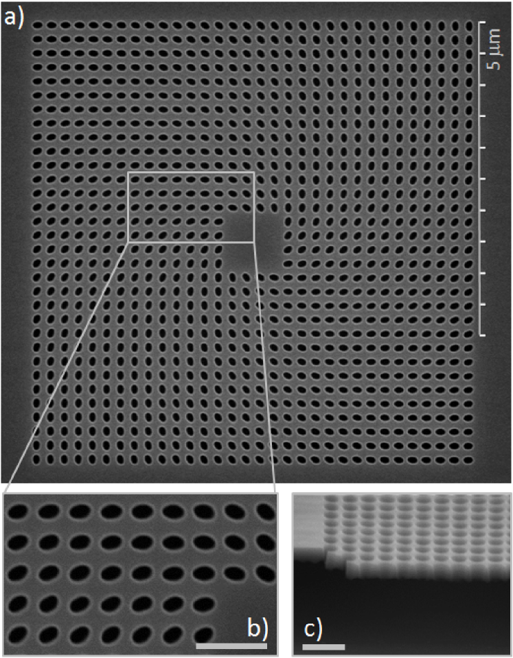
Figure 1 shows a topological defect laser that was fabricated. A 190-nm-thick GaAs layer and a 1000-nm thick Al0.75Ga0.25As layer were grown on a GaAs substrate by molecular beam epitaxy. Inside the GaAs layer, three uncoupled layers of InAs QDs, equally spaced by 25 nm GaAs barriers, were embedded. The two-dimensional (2D) array of air holes was fabricated in the GaAs layer by electron-beam lithography and reactive ion etching [Fig. 1(a)]. The Al0.75Ga0.25As layer was then etched to leave a free-standing GaAs membrane in air [Fig. 1(c)]. As seen in Fig. 1(a,b), the angle between the major axis of an ellipse and the -axis was set to , where denotes the polar angle of the center position of the ellipse, is the topological charge, and . air holes were removed from the center of the topological defect, which coincides with the center of the array, to create localized states in analogy to the regular PhC defect states. We have fabricated many patterns of different structural parameters, e.g., the lattice constant , the filling fraction, and the ellipticity (the ratio of the major axis over the minor axis of the ellipse) of air holes. By changing , we were able to tune the wavelength of the high- defect-modes into the gain spectrum of InAs QDs to induce lasing action. We also varied to gradually change the strength of the topological defect and monitor its effect on lasing. In the special case of , the structure becomes a regular photonic crystal of circular air holes Ryu et al. (2002).
In the lasing experiments, the samples were optically pumped by a mode-locked Ti:Sapphire laser (pulse duration 200 fs, center wavelength 790 nm, and pulse repetition rate 76 MHz). Optical measurements were carried out in a cryostat at = 10 K, to maximize the optical gain of InAs QDs. A long working distance objective lens ( magnification, 0.4 numerical aperture) was used to focus the pump light to the structure at normal incidence. The emission from the sample was collected by the same objective lens and directed to a grating (600 lines/mm) spectrometer with a cooled charged coupled device (CCD) array detector (resolution 0.3 nm).
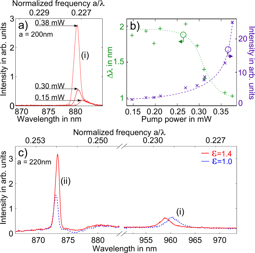
Lasing was observed in the topological defect structure with = 200 nm and . Figure 2(a) shows an emission peak at nm that grows with pump power. Its spectrally-integrated intensity, plotted as a function of the incident pump power in Fig. 2(b), exhibits a threshold behavior. When exceeds 0.3 mW, the peak intensity increases much more rapidly with pump power, meanwhile its linewidth decreases abruptly. This behavior indicates the onset of lasing action. The relatively broad linewidth of 1 nm above the lasing threshold is caused by the hot carrier effect. Due to short pulse pumping, the density of electron-hole pairs varies in time, causing a change in the value of refractive index and a shift of lasing frequency Pompe et al. (1995); Jahnke and Koch (1995). This transient frequency shift results in a broadening of the lasing line in the time-integrated measurement of the emission spectrum.
To tune the lasing frequency, we increase the lattice constant to 220 nm while keeping the filling fraction of air holes fixed. As shown in Fig. 2(c), the emission peak at 880 nm shifts to 960 nm. The normalized frequency remained constant, consistent with the scaling of the structure size. Due to relatively weak gain at 960 nm, this mode [labeled (i) in Fig. 2(c)] no longer lased. Instead, another mode [labeled (ii) in Fig. 2(c)] started lasing at = 873 nm. From its normalized frequency , we infer its wavelength in the previous structure with = 200 nm to be = 800 nm, which falls outside the gain spectrum. Therefore this mode could not have lased previously.
We also observed lasing in the samples of and 1.0. With the same lattice constant and filling fraction of air holes, the lasing frequencies are similar to those in the samples with . As an example, Fig. 2(c) includes the emission spectrum of a sample with the same but = 1.0 (circular air holes).
To understand the difference in the lasing modes between the topological defect structures and regular photonic crystals, we performed numerical calculations using the 3D finite-difference frequency-domain (FDFD) method Comsol (2014). With the addition of optical gain, the high- modes of the passive system, whose frequencies fall within the gain spectrum, reach the lasing threshold first, and their characteristic remains nearly unchanged above threshold. Therefore, the simulated resonances of the passive structures can be identified with the lasing modes that were observed experimentally. Only transverse-electric (TE) polarized modes were computed, because the QDs in the fabricated samples provide stronger amplification for light with this polarization. Due to limited computing resources, the size of air hole array was reduced to . All other structural parameters used in the simulations are identical to those of the fabricated samples.
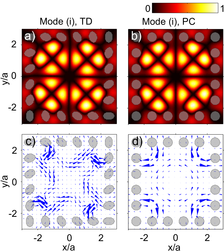
In the numerical simulation, we identify the high- modes that correspond to the lasing modes observed experimentally. Fig. 3(a) shows the calculated field profile for a defect mode of normalized frequency = 0.23, which coincides with that of the lasing mode (i) in Fig. 2(a). The ellipticity of the air holes is = 1.4. The mode quality factor is = . For comparison, we calculated the same mode in the regular PhC with circular holes ( = 1.0), as shown in Fig. 3(b). The mode profile remains nearly unchanged when the ellipticity of air holes is reduced from 1.4 to 1.0. However, the energy flow pattern changes significantly, as seen in the spatial map of the Poynting vector in Fig. 3(c,d). Each arrow points in the direction of local energy flux, and its size is proportional to the amplitude of the flux. For the regular photonic crystal defect state, the energy flows out of the central defect region [Fig. 3(c)]. In the presence of the topological defect, the optical flux circulates clockwise (CW) in the central region [Fig. 3(d)].
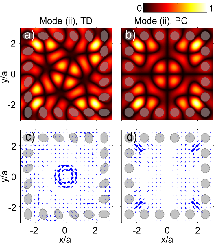
Figure 4(a) shows the calculated field profile for another defect mode at the normalized frequency = 0.25, which coincides with that of the lasing mode (ii) in Fig. 2(c). Unlike the mode at = 0.23, this mode shows a notable change in the field profile when the ellipticity of the air holes is changed between 1.0 and 1.4 [4(a,b)]. More specifically, the field pattern rotates clockwise (CW) when increases from 1.0 to 1.4. The spatial map of the Poynting vector in Fig. 4(c,d) reveals a much more dramatic change in the energy flow. In the PhC defect state, the energy flows mostly outward through the four corners of the defect region. In contrast, a CW circulating flux pattern arises in the center of a topological defect, indicating the formation of an optical vortex. The lateral dimension of the vortex is about one lattice constant (), which is a quarter of the vacuum wavelength ().
The drastic change in the energy flow is attributed to the spatial variation of the ellipse orientation in the topological defect structure. As seen in Fig. 1(a), the topological defect structure consists of four crystalline domains located in the four quadrants. The ellipses in each quadrant are aligned almost in the same direction, but they are rotated 90 degree from one quadrant to the next. Light can leak out of the central defect region by in-plane escape through the boundary and out-of-plane scattering. The in-plane leakage relies on the coupling between the defect state and the propagating modes in the surrounding lattice. The rotation of the crystalline domains breaks the balance in the out-coupling of CW and CCW waves in the defect region. For example, if the CCW wave experiences more out-coupling than the CW wave, the net energy flow inside is CW Liew et al. (2014).
In summary, we experimentally realized a topological defect laser. By introducing the disclination to a 2D photonic crystal with anisotropic unit cell, we obtain spatially confined optical resonances with high quality factor. Such resonances, unlike the regular photonic crystal defect states, support powerflow vortices. In the presence of optical gain, these modes can lase, and their frequencies may be tuned by the structural parameters. This work shows that the spatially inhomogeneous variation of the unit cell orientation adds another dimension to the control of a lasing mode, enabling the manipulation of its field pattern and energy flow landscape.
We thank Yaron Bromberg, Eric Dufresne and Chinedum Osuji for useful discussions. This work is supported by the MURI grant No. N00014-13-1-0649 from the US Office of Naval Research and by the NSF under the Grant No. DMR-1205307.
References
- Senyuk et al. (2013) B. Senyuk, Q. Liu, S. He, R. D. Kamien, R. B. Kusner, T. C. Lubensky, and I. I. Smalyukh, Nature 493, 200 (2013).
- Muševič (2013) I. Muševič, Phil. Trans. R. Soc. A 371, 20120266 (2013).
- Loussert et al. (2013) C. Loussert, U. Delabre, and E. Brasselet, Phys. Rev. Lett. 111, 037802 (2013).
- Brasselet and Loussert (2011) E. Brasselet and C. Loussert, Opt. Lett. 36, 719 (2011).
- Brasselet (2010) E. Brasselet, Phys. Rev. A 82, 063836 (2010).
- Barboza et al. (2012) R. Barboza, U. Bortolozzo, G. Assanto, E. Vidal-Henriquez, M. G. Clerc, and S. Residori, Phys. Rev. Lett. 109, 143901 (2012).
- Barboza et al. (2013) R. Barboza, U. Bortolozzo, G. Assanto, E. Vidal-Henriquez, M. Clerc, and S. Residori, Phys. Rev. Lett. 111, 093902 (2013).
- Brasselet et al. (2009) E. Brasselet, N. Murazawa, H. Misawa, and S. Juodkazis, Phys. Rev. Lett. 103, 103903 (2009).
- Smalyukh et al. (2007) I. I. Smalyukh, D. S. Kaputa, A. V. Kachynski, A. N. Kuzmin, and P. N. Prasad, Opt. Expr. 15, 4359 (2007).
- Brasselet et al. (2008) E. Brasselet, N. Murazawa, S. Juodkazis, and H. Misawa, Phys. Rev. E 77, 041704 (2008).
- Soukoulis (2001) C. M. Soukoulis, Photonic crystals and light localization in the 21st century, Vol. 563 (Springer, 2001).
- Noda and Baba (2003) S. Noda and T. Baba, Roadmap on photonic crystals, Vol. 1 (Springer, 2003).
- Sakoda (2005) K. Sakoda, Optical properties of photonic crystals, Vol. 80 (Springer, 2005).
- Joannopoulos et al. (2011) J. D. Joannopoulos, S. G. Johnson, J. N. Winn, and R. D. Meade, Photonic crystals: molding the flow of light (Princeton university press, 2011).
- Painter et al. (1999a) O. Painter, R. Lee, A. Scherer, A. Yariv, J. O’brien, P. Dapkus, and I. Kim, Science 284, 1819 (1999a).
- Painter et al. (1999b) O. Painter, A. Husain, A. Scherer, J. O’Brien, I. Kim, and P. Dapkus, J. Lightwave Technol. 17, 2082 (1999b).
- Park et al. (2001) H.-G. Park, J.-K. Hwang, J. Huh, H.-Y. Ryu, Y.-H. Lee, and J.-S. Kim, Appl. Phys. Lett. 79, 3032 (2001).
- Ryu et al. (2002) H.-Y. Ryu, S.-H. Kim, H.-G. Park, J.-K. Hwang, Y.-H. Lee, and J.-S. Kim, Appl. Phys. Lett. 80, 3883 (2002).
- Pompe et al. (1995) G. Pompe, T. Rappen, M. Wehner, F. Knop, and M. Wegener, Phys. Status Solidi B 188, 175 (1995).
- Jahnke and Koch (1995) F. Jahnke and S. W. Koch, Phys. Rev. A 52, 1712 (1995).
- Comsol (2014) Comsol, “Multiphysics 4.4,” (2014).
- Liew et al. (2014) S. F. Liew, S. Knitter, W. Xiong, and H. Cao, arXiv preprint arXiv:1411.4948 (2014).