Critical Behavior of a Strongly Disordered 2D Electron System:
The Cases of Long-Range and Screened Coulomb Interactions
Abstract
A study of the temperature () and density () dependence of conductivity of a highly disordered, two-dimensional (2D) electron system in Si demonstrates scaling behavior consistent with the existence of a metal-insulator transition (MIT). The same critical exponents are found when the Coulomb interaction is screened by the metallic gate and when it is unscreened or long range. The results strongly suggest the existence of a disorder-dominated 2D MIT, which is not directly affected by the range of the Coulomb interactions.
pacs:
71.30.+h, 73.40.Qv, 71.27.+aThe metal-insulator transition (MIT) in 2D systems remains one of the most fundamental open problems in condensed matter physics 2DMIT-review_2001 ; 2DMIT-review_2004 ; 2DMIT-review_2010 . There is considerable experimental evidence that suggests that electron-electron interactions are responsible for a variety of phenomena observed in the metallic regime of low-disorder 2D systems near the apparent MIT, including a large increase of conductivity with decreasing temperature () Radonjic . Many-body effects have been most pronounced in a 2D electron system (2DES) in Si metal-oxide-semiconductor field-effect transistors (MOSFETs). Since the most striking experimental features are not sensitive to weak disorder (see, e.g., the thermopower study in Ref. Kravchenko-thermo ), they have been interpreted as evidence that the MIT in such low-disorder systems is driven by electron-electron interactions and that disorder has only a minor effect. In highly disordered systems, on the other hand, is usually not observed. However, careful studies of ( – the electron density) and glassy charge dynamics in a 2DES in Si have provided ample evidence for the MIT and for the importance of long-range Coulomb interactions also in these systems DP-CIQPT . The following key questions thus arise: (1) What is the nature of the MIT in a high-disorder 2DES with interactions? More precisely, is it dominated by disorder, or is it the same as the MIT in a low-disorder 2DES, which is believed to be driven by interactions? (2) What is the effect of the range of electron-electron interactions on the MIT in a high-disorder 2DES?
Here we report a study of in high-disorder 2DES in Si MOSFETs, which demonstrates scaling behavior consistent with the existence of a quantum phase transition (QPT). Measurements were done on devices in which the long-range part of the Coulomb interaction is screened by the metallic gate. Scaling analysis was also performed on another sample of the same type, studied previously Bogdanovich and Popović (2002); Jaroszyński and Popović (2006, 2007a, 2007b); Jaroszynski2009466 ; Lin et al. (2012), but in which the electron-electron interaction is long range. The comparison of our results to those on low-disorder systems provides clear evidence that sufficiently strong disorder changes the universality class of the MIT. We also find that, in such a disorder-dominated transition, the range of the Coulomb interactions does not appear to affect the critical exponents.
The use of a nearby metallic gate or ground plane to limit the range of the Coulomb interactions between charge carriers in 2D systems is a well-known technique that has been explored both theoretically (see, e.g., Peeters1984 ; Widom and Tao (1988); Hallam et al. (1996); Ho et al. (2009); Skinner-Shk ; Skinner and Fogler (2010); Fregoso and Sá de Melo (2013)) and experimentally, e.g. in the investigation of the melting of the Wigner crystal formed by electrons on a liquid He surface Mistura et al. (1997). In the context of the 2D MIT, it has been used to explore the role of Coulomb interactions in the metallic Ho et al. (2008) and insulatorlike Huang2014 regimes of a 2D hole system (2DHS) in “clean”, i.e. low-disorder AlGaAs/GaAs heterostructures and in the metallic regime of low-disorder Si MOSFETs Tracy . In contrast, we report on the screening by the metallic gate in a high-disorder 2D system. Our conclusions are based on behavior on both metallic and insulating sides of the MIT.
The metallic gate at a distance from the 2DES creates an image charge for each electron, modifying the Coulomb interaction from to . When the mean carrier separation , this potential falls off in a dipolelike fashion, as . Therefore, in Si MOSFETs, the range of the electron-electron Coulomb interactions can be changed by varying the thickness of the oxide . Our study was performed on two sets of Si MOSFETs that were fabricated simultaneously using the 0.25-m Si technology Taur , the only difference being the value of . In “thick-oxide” samples, nm, comparable to that in other Si MOSFETs used in the vast majority of studies of the 2D MIT 2DMIT-review_2001 ; 2DMIT-review_2004 ; 2DMIT-review_2010 ; DP-CIQPT . In the low- regime of interest near the MIT, the corresponding . On the other hand, in our “thin-oxide” devices with nm, substantial screening by the gate is expected in the scaling regime of near the MIT, where . For comparison, in other ground-plane screening studies, in Ref. Tracy , in Ref. Huang2014 , and in Ref. Ho et al. (2008).
The samples were rectangular n-channel (100)-Si MOSFETs with poly-Si gates, self-aligned ion-implanted contacts, and oxide charge cm-2. We focus on two samples that are representative of the two sets of devices: sample Bthin, with nm, substrate doping cm-3, and dimensions m2 ( – length, – width); sample A1 with nm, cm-3, and m2 Bogdanovich and Popović (2002); Lin et al. (2012). In analogy with previous studies on thick-oxide devices Bogdanovich and Popović (2002); Jaroszyński and Popović (2006, 2007a, 2007b); Jaroszynski2009466 ; Lin et al. (2012), the substrate (back-gate) bias of V was applied, resulting in a 4.2 K peak mobility of m2/Vs and m2/Vs for Bthin and A1, respectively. Such low values of reflect the presence of a large amount of disorder. Detailed measurements were performed on sample Bthin; the previously obtained data on A1 Bogdanovich and Popović (2002) were also analyzed.
was measured using a standard two-probe ac method at Hz with an ITHACO 1211 current preamplifier and a SR7265 lock-in amplifier in a 3He system (base K). The contact resistances and the contact noise were determined to be negligible relative to those of the 2DES, as described in Ref. Bogdanovich and Popović (2002). The excitation voltage was constant and low enough (V) to ensure that the conduction was Ohmic. A precision dc voltage standard (EDC MV116J) was used to apply the gate voltage , which controls : cmV for sample Bthin. Similar to studies of thick-oxide devices Bogdanovich and Popović (2002); Jaroszyński and Popović (2006, 2007a, 2007b); Jaroszynski2009466 ; Lin et al. (2012), was varied at K EF-note , followed by cooling to a desired with a fixed . was measured as a function of time, up to several hours at the lowest and . Some sweeps using a HP3325B function generator were also performed to verify that K was (a) high enough for the 2DES to be in a thermal equilibrium, as there were no visible relaxations, and (b) low enough for the background potential (disorder) to remain unchanged, as evidenced by the reproducible fluctuations of at low . The study of fluctuations with or with time, however, is beyond the scope of this work. Here we focus instead on the behavior of the average conductivity Mirlin .
Figure 1(a) shows as a function of for different near the MIT, as discussed below. In general, the behavior of is similar to that in thick-oxide devices Bogdanovich and Popović (2002); Lin et al. (2012), although the absolute values of for the same and are lower here. We note that the mere decrease of with decreasing (i.e. ) at a given does not necessarily imply the existence of an insulating state (). Indeed, the existence of a 2D metal with has been already demonstrated in three different types of 2DES in Si MOSFETs: 1) in the presence of scattering by disorder-induced local magnetic moments, both in zero magnetic field ()Feng et al. (2001) and in parallel Eng2002 ; 2) in low-disorder samples in parallel Jan2004 ; and 3) in high-disorder, thick-oxide samples () Bogdanovich and Popović (2002). Therefore, , the critical density for the MIT, in our high-disorder, thin-oxide system [Fig. 1(a)] also has to be determined from the fits to on both metallic and insulating sides of the transition.

(a)
 (b)
(b)
For the lowest and , the best fit to the data is obtained with [Fig. 1(b)], which corresponds to the 2D Mott variable-range hopping (VRH). The vanishing of the activation energy, as extrapolated from the insulating phase, is often used as a criterion to determine (see, e.g., Refs. Pudalov-nc ; Shashkin-nc ; Bogdanovich and Popović (2002); Jan2002 ; Jan2004 ). Here the extrapolation of to zero (Fig. 1(b) inset) yields cm-2.
For , the low- data are best described by the metallic () power law [Fig. 2(a)]. The same non-Fermi-liquid correction was observed in the metallic, glassy phase (; - glass transition density) of both thick-oxide, high-disorder samples at Bogdanovich and Popović (2002) and low-disorder 2DES in parallel Jan2004 , consistent with theoretical predictions Dalidovich ; Sachdev-2012 . This simple and precise form of allows a reliable extrapolation to [Fig. 2(a)]. The extrapolated go to zero at cm2 [Fig. 2(b)], in agreement with the value obtained from the VRH fit. Moreover, a simple power-law dependence found here (Fig. 2(a); ), is consistent with the one expected in the quantum critical region of the MIT based on general arguments Belitz-RMP . Likewise, the power-law behavior [Fig. 2(c)] is in agreement with theoretical expectations near a QPT, such as the MIT. The critical exponent .


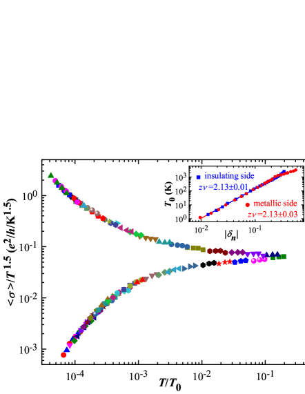
In addition, very general considerations have suggested Belitz-RMP that the conductivity near the MIT can be described by a scaling form , where and are the dynamical and correlation length exponents, respectively, and the critical conductivity . Figure 3 shows that, in the vicinity of , all collapse onto the same function with two branches: the upper one for the metallic side of the transition and the lower one for the insulating side. As expected for a QPT, the scaling parameter is the same, power-law function of on both sides of the transition, (Fig. 3 inset), with within experimental error.

From standard scaling arguments Belitz-RMP , it follows that the critical exponent can be determined not only from extrapolations of to [Fig. 2(c)], but also from based on all data taken at all and values of for which scaling holds. Indeed, using (Figs. 2(a) and 3) and (Fig. 3 inset), we find the value that is in excellent agreement with found from the extrapolation of . This confirms the consistency of the analysis.
In a similar way, we analyze near cm2 in a thick-oxide, high-disorder MOSFET Bogdanovich and Popović (2002), in which the electron-electron interaction is long range. Figure 4 demonstrates that, near , the data exhibit dynamical scaling, a signature of the QPT, also in this system. The scaling parameter (Fig. 4 inset), with within experimental error. Therefore, the critical exponents are the same as those in thin-oxide, high-disorder samples, and thus not sensitive to the range of the Coulomb interactions.
The critical exponents have been summarized in Table 1. The Table also shows critical exponents obtained in 2DESs with much lower disorder (i.e. high ) Kravchenko et al. (1995, 1996); Popović et al. (1997); Pudalov et al. (1998); Feng et al. (1999); Jan2004 ; Ted-Belitz-2013 ; Fletcher et al. (2001), including those in which scattering by local magnetic moments dominates Feng et al. (2001); Eng2002 . The values obtained in low parallel (i.e. not high enough to fully spin polarize the 2DES spin-polarization1 ; spin-polarization2 ) are also included, where available. It is apparent that such low fields do not seem to affect any of the critical exponents. On the other hand, we find a major difference between in our low- devices and, consistently lower, in high- 2DES Kravchenko et al. (1995, 1996); Popović et al. (1997); Pudalov et al. (1998); Feng et al. (1999, 2001); Ted-Belitz-2013 . This result indicates that sufficiently strong disorder changes the nature of the MIT from interaction-driven in high- samples to disorder-dominated in low- 2DES. In such a disorder-dominated MIT, it is plausible that the range of the Coulomb interactions does not seem to play a major role. The possibility of a disorder-dominated 2D MIT has been demonstrated theoretically Punnoose for both long-range and short-range interactions. Although there is currently no microscopic theory that describes the detailed properties of the observed MIT, it is interesting that in the available theories Belitz-RMP ; Punnoose , the range of the Coulomb interactions does not play a significant role. We also note that percolation models percolation cannot describe our findings, e.g. the 2D percolation , as opposed to the much larger experimental (Table 1). Interestingly, the same large was observed in a high- 2DES () in the presence of scattering by local magnetic moments Feng et al. (2001). Therefore, unlike , the exponent seems to be more sensitive to the type (e.g. magnetic vs. nonmagnetic), rather than to the amount of disorder.
High-disorder system Special disorder: local magnetic moments Low-disorder system thin oxide thick oxide 0.04 0.06 6.9 50 43.5 40-600 Feng et al. (2001) Eng2002 0.5-1 – Jan2004 Kravchenko et al. (1995, 1996); Popović et al. (1997); Pudalov et al. (1998); Feng et al. (1999); Ted-Belitz-2013 – – 1-1.5 Fletcher et al. (2001) Jan2004 – –
Our study demonstrates the critical behavior of consistent with the existence of a metal-insulator quantum phase transition in a highly disordered 2DES in Si MOSFETs. The results strongly suggest that, in contrast to the MIT in a low-disorder 2DES, the MIT reported here is dominated by disorder. We have also established that the range of the Coulomb interactions does not seem to affect the properties, i.e. the critical exponents, of such a disorder-dominated MIT. On the other hand, the effect of the range of electron-electron interactions on the critical behavior of a low-disorder 2DES remains an open question.
The authors acknowledge the IBM T. J. Watson Research Center for fabricating the devices and V. Dobrosavljević for useful discussions. This work was supported by NSF grants DMR-0905843, DMR-1307075, and the National High Magnetic Field Laboratory through NSF Cooperative Agreement DMR-1157490 and the State of Florida.
References
- (1) E. Abrahams, S. V. Kravchenko, and M. P. Sarachik, Rev. Mod. Phys. 73, 251 (2001).
- (2) S. V. Kravchenko and M. P. Sarachik, Rep. Prog. Phys. 67, 1 (2004).
- (3) B. Spivak, S. V. Kravchenko, S. A. Kivelson, and X. P. A. Gao, Rev. Mod. Phys. 82, 1743 (2010).
- (4) M. M. Radonjić, D. Tanasković, V. Dobrosavljević, K. Haule, and G. Kotliar, Phys. Rev. B 85, 085133 (2012).
- (5) A. Mokashi, S. Li, B. Wen, S. V. Kravchenko, A. A. Shashkin, V. T. Dolgopolov, and M. P. Sarachik, Phys. Rev. Lett. 109, 096405 (2012).
- (6) For a review, see D. Popović in Conductor-Insulator Quantum Phase Transitions, edited by V. Dobrosavljević, N. Trivedi, and J.M. Valles Jr. (Oxford University Press, Oxford, 2012).
- Bogdanovich and Popović (2002) S. Bogdanovich and D. Popović, Phys. Rev. Lett. 88, 236401 (2002).
- Jaroszyński and Popović (2006) J. Jaroszyński and D. Popović, Phys. Rev. Lett. 96, 037403 (2006).
- Jaroszyński and Popović (2007a) J. Jaroszyński and D. Popović, Phys. Rev. Lett. 99, 046405 (2007a).
- Jaroszyński and Popović (2007b) J. Jaroszyński and D. Popović, Phys. Rev. Lett. 99, 216401 (2007b).
- (11) J. Jaroszyński and D. Popović, Physica B 404, 466 (2009).
- Lin et al. (2012) P. V. Lin, X. Shi, J. Jaroszynski, and D. Popović, Phys. Rev. B 86, 155135 (2012).
- (13) F. M. Peeters, Phys. Rev. B 30, 159 (1984).
- Widom and Tao (1988) A. Widom and R. Tao, Phys. Rev. B 38, 10787 (1988).
- Hallam et al. (1996) L. D. Hallam, J. Weis, and P. A. Maksym, Phys. Rev. B 53, 1452 (1996).
- Ho et al. (2009) L. H. Ho, A. P. Micolich, A. R. Hamilton, and O. P. Sushkov, Phys. Rev. B 80, 155412 (2009).
- (17) B. Skinner and B. I. Shklovskii, Phys. Rev. B 82, 155111 (2010).
- Skinner and Fogler (2010) B. Skinner and M. M. Fogler, Phys. Rev. B 82, 201306(R) (2010).
- Fregoso and Sá de Melo (2013) B. M. Fregoso and C. A. R. Sá de Melo, Phys. Rev. B 87, 125109 (2013).
- Mistura et al. (1997) G. Mistura, T. Günzler, S. Neser, and P. Leiderer, Phys. Rev. B 56, 8360 (1997).
- Ho et al. (2008) L. H. Ho, W. R. Clarke, A. P. Micolich, R. Danneau, O. Klochan, M. Y. Simmons, A. R. Hamilton, M. Pepper, and D. A. Ritchie, Phys. Rev. B 77, 201402(R) (2008).
- (22) J. Huang, L. N. Pfeiffer, and K. W. West, Phys. Rev. Lett. 112, 036803 (2014).
- (23) L. A. Tracy, E. H. Hwang, K. Eng, G. A. Ten Eyck, E. P. Nordberg, K. Childs, M. S. Carroll, M. P. Lilly, and S. Das Sarma, Phys. Rev. B 79, 235307 (2009).
- (24) Y. Taur and T. H. Ning, Fundamentals of Modern VLSI Devices (Cambridge University Press, Cambridge, 1999).
- (25) F. Evers and A. D. Mirlin, Rev. Mod. Phys. 80, 1355 (2008).
- (26) The Fermi temperature Kcm for electrons in Si MOSFETs AFS .
- (27) T. Ando, A. B. Fowler, and F. Stern, Rev. Mod. Phys. 54, 437 (1982).
- Feng et al. (2001) X. G. Feng, D. Popović, S. Washburn, and V. Dobrosavljević, Phys. Rev. Lett. 86, 2625 (2001).
- (29) K. Eng, X. G. Feng, D. Popović, and S. Washburn, Phys. Rev. Lett. 88, 136402 (2002).
- (30) J. Jaroszyński, D. Popović, and T. M. Klapwijk, Phys. Rev. Lett. 92, 226403 (2004).
- (31) V. M. Pudalov, M. D’Iorio, S. V. Kravchenko, and J. W. Campbell, Phys. Rev. Lett. 70, 1866 (1993).
- (32) A. A. Shashkin, S. V. Kravchenko, and T. M. Klapwijk, Phys. Rev. Lett. 87, 266402 (2001).
- (33) J. Jaroszyński, D. Popović, and T. M. Klapwijk, Phys. Rev. Lett. 89, 276401 (2002).
- (34) D. Dalidovich and V. Dobrosavljević, Phys. Rev. B 66, 081107 (2002).
- (35) M. Müller, P. Strack, and S. Sachdev, Phys. Rev. A 86, 023604 (2012).
- (36) D. Belitz and T. R. Kirkpatrick, Rev. Mod. Phys. 66, 261 (1994).
- (37) V. T. Dolgopolov, G. V. Kravchenko, A. A. Shashkin, and S. V. Kravchenko, JETP Lett. 55, 733 (1992).
- (38) M. R. Sakr, M. Rahimi, and S. V. Kravchenko, Phys. Rev. B 65, 041303(R) (2001).
- Kravchenko et al. (1995) S. V. Kravchenko, W. E. Mason, G. E. Bowker, J. E. Furneaux, V. M. Pudalov, and M. D’Iorio, Phys. Rev. B 51, 7038 (1995).
- Kravchenko et al. (1996) S. V. Kravchenko, D. Simonian, M. P. Sarachik, W. Mason, and J. E. Furneaux, Phys. Rev. Lett. 77, 4938 (1996).
- Popović et al. (1997) D. Popović, A. B. Fowler, and S. Washburn, Phys. Rev. Lett. 79, 1543 (1997).
- Pudalov et al. (1998) V. Pudalov, G. Brunthaler, A. Prinz, and G. Bauer, JETP Lett. 68, 442 (1998).
- Feng et al. (1999) X. G. Feng, D. Popović, and S. Washburn, Phys. Rev. Lett. 83, 368 (1999).
- (44) T. R. Kirkpatrick and D. Belitz, Phys. Rev. Lett. 110, 035702 (2013).
- Fletcher et al. (2001) R. Fletcher, V. M. Pudalov, A. D. B. Radcliffe, and C. Possanzini, Semicond. Sci.. Tech. 16, 386 (2001).
- (46) T. Okamoto, K. Hosoya, S. Kawaji, and A. Yagi, Phys. Rev. Lett. 82, 3875 (1999).
- (47) S. A. Vitkalov, H. Zheng, K. M. Mertes, M. P. Sarachik, and T. M. Klapwijk, Phys. Rev. Lett. 85, 2164 (2000).
- (48) A. Punnoose and A. M. Finkel’stein, Science 310, 289 (2005).
- (49) See, for example, D. Stauffer and A. Aharony, Introduction to Percolation Theory (Taylor & Francis, London, 1994).