Inductance extraction of superconductor structures with internal current sources
Abstract
The sheet current model underlying the software 3D-MLSI package for calculation of inductances of multilayer superconducting circuits, has been further elaborated. The developed approach permits to overcome serious limitations on the shape of the circuits layout and opens the way for simulation of internal contacts or vias between layers. Two models for internal contacts have been considered. They are a hole as a current terminal and distributed current source. Advantages of the developed approach are illustrated by calculating the spatial distribution of the superconducting current in several typical layouts of superconducting circuits. New meshing procedure permits now to implement triangulation for joint projection of all nets thus improving discrete physical model for inductance calculations of circuits made both in planarized and non-planarized fabrication processes. To speed-up triangulation and build mesh of better quality, we adopt known program ”Triangle”.
I Introduction
The challenges Anders et al., (2010); IAR, (2014) facing the development of the modern digital superconducting electronics urgently require not only the development of new technological solutions Tolpygo et al., 2014b ; Tolpygo et al., 2014a ; Nagasawa et al., (2009); Fujimaki et al., (2014); Nagasawa et al., (2014) but also new tools needed to calculate inductances, resulting in topological configurations of designed digital cells. Inductances are the important component of all superconductor digital circuits. Calculation of inductances, currents and fields for layouts in superconductor electronics is important and challenging problem Gaj et al., (1999); Fourie and Volkmann, (2013). Currently several programs are used for inductances calculations Bunyk and Rylov, (1993); Fourie et al., (2011); Khapaev et al., (2001). These programs are intended for different areas Fourie and Volkmann, (2013) and utilize different superconducting current models. Recently it was demonstrated Tolpygo et al., (2014) that 3-D inductance extractors based on FastHenry Fourier, (2014); Kamon M. and J.K., (1994); Whiteley, (2014) and 3D-MLSI Khapaev, (2001); Khapaev and Kupriyanov, 2010a software can be successfully used for calculations of inductance of various superconducting microstrip-line and stripline inductors having linewidth down to 250 nm in 8-metal layer process developed for fabricating VLSI superconductor circuits.
Unfortunately, the existing inductances extraction tools have some limitations. Lmeter Bunyk and Rylov, (1993) do not apply, if parts of a film or a wire in a multilayer structure don’t have strong magnetic coupling with other layers in the structure. For example, Lmeter can’t be used for single layer structures and structures without groundplanes. FastHenry tool Fourie, (2013) needs accuracy calibration and meets problems for holes and groundplanes. It is difficult to use 3D-MLSI Khapaev, (2001) for quantitative and qualitative description of the effects caused by current injection through the internal terminals located inside multilayer structures. These terminals are staggered or stacked vias between layers Tolpygo et al., (2014) or connections between the films contained Josephson junction.
In this paper we attack these problems by improvement of our 3D-MLSI software aimed on removing limitations on using the internal terminals. To do that we introduce two new models for current sources and improve the accuracy of our numerical algorithm and program by using the new scheme of FEM triangular meshing aligned to all film boundaries. The scheme allows to do more accurate calculations for non-planarized circuits and has as an option allowing us to use an external program Triangle Shewchuk, (1996) for FEM mesh construction.
In the first model of internal terminal we declare a hole or any part of hole in a multilayer film as current terminal and define inlet or outlet current on its perimeter. This new current terminal is almost identical to a similar terminal located at the external borders of the film. However, there is the difference. It consists in the fact that the new mutual inductance between current around the hole and current from hole appears.
The first model doesn’t allow a current flows under the contact. It isn’t applicable if there are two contacts on same place from top and from bottom of the film. In these cases it is convenient to use the second internal terminal model. We call it ”hole as a current source”.
In the second model, the area of the film, which is located under the contact (via) is not cut out. It remains an integral part of the film, in which we solve the equations that determine the spatial distribution of the current. These equations are properly modified to include current sources located in the area of inner terminals. The total current provided by the current source is the given value.
Advantages of the developed approach are illustrated in the last sections of the paper by calculation of the spatial distribution of the superconducting current in several typical layouts of superconducting circuits.
II Basic Assumptions
We consider multilayer, planar, multi-connected structures, which consist of superconducting (S) films separated by dielectric interlayers. The design can have or have not ground plane that reside under all wires. There are no restrictions on floor plane shapes of the S films. They can contain holes, current terminals on external boundary and current terminals (contacts) in inner areas of S layers. Current distribution in the film can be induced by different sources. These sources can be given full currents circulating around holes or fluxoids trapped in the holes, given full currents between external or internal contacts, and external magnetic field.
A single S film with one hole and three current terminals (contacts) is shown in Fig. 1. It will be used to illustrate new features of the presented version of our 3D-MLSI package. The hole on Fig. 1 traps zero or non-zero flux. Internal contacts can model Josephson junctions, as well as staggered or stacked vias between S layers. Terminal on external boundary (dashed segment) models external wire.
For further convenience, let , stands for points in 3D space, , - for points on 2D plane. Also, consider differential operators , , , . is Laplace operator in 3D and is Laplace operators in 2D space.
III Mathematical Model
Rigorous electromagnetic analysis should be started from stationary Maxwell and London equations Orlando and Delin, (1991); Duzer and Turner, (1999):
| (1) | |||
| (2) |
where is London penetration depth, is magnetic field of current is external magnetic field. Equations (1), (2) can be rewritten in the form of volume current integral equations using vector potential, for magnetic field
| (3) | |||
| (4) |
Here integration is performed over the volume of all conductors, is a scalar function, which is proportional to phase of superconductor condensate function.
Equations (3), (4) together with appropriate boundary conditions can be solved numerically. Typically, to do that the PEEC (Partial Element Equivalent Circuit) method is used. This method was evaluated for normal conductors Ruehli, (1974), enhanced for large problems Kamon M. and J.K., (1994) and recently adopted for superconductors Whiteley, (2014); Fourie et al., (2011).
Boundary conditions for Eqs. (3), (4) are easy formulated for wire-like conductors with external or internal current terminals. Description of holes with trapped fluxoids and large flat structures like ground planes meets some difficulties in using these PEEC-like methods. For superconductors it can cause accuracy, memory and performance problems.
Our approach is based on some assumptions concerning dimensions of the circuits. We assume that floor plan dimensions are much larger than the film thicknesses that in turn are less or of the order of London penetration depth. In this case, the volume current density in superconductor can be accurately approximated by a sheet current density. If the assumptions are violated then the accuracy of our approach is reduced. Nevertheless, the method provides sufficient accuracy of calculation in the case where the film thickness is about 2 - 3 penetration depths Khapaev, (2001).
Planarity assumptions allow us to introduce sheet current . Let is the thickness of the layer (see Fig. 1) and is London penetration depth for films. We assume that and take average volume current density over the film thickness (Fig. 1):
| (5) |
Then from (3) it follows that satisfies the integral equation:
| (6) | |||
| (7) |
Kernel is result of averaging procedure for (3). For single layer problems it can be taken simply as
| (8) |
For multilayer structures with layers and and heights Khapaev, (2001)
| (9) |
On the next step it is convenient to introduce the stream function
| (10) |
and rewrite (6) in the form Khapaev, (2001)
| (11) |
Here is component of external magnetic field oriented in direction. For very thin conductors can be taken in the form (8).
Equation (11) should be supplemented by boundary conditions. These boundary conditions are simple first kind boundary conditions since values of stream function on the boundary are known Khapaev, (2001):
| (12) | |||
| (13) |
Here is the full current circulating around hole with boundary . On the external boundary function can be easily evaluated using well-known properties of stream function.
Mathematically problem (11), (12), (13) is very similar to boundary problem for Poisson equation. We prefer to solve equation (11) instead of (6) since (11) easily accounts currents circulating around holes and for reasons of efficiency of numerical computations. After calculation of the function, we can calculate the energy functional, as well as the inductance matrix Khapaev, (2001).
Unfortunately -function approach meets problems for structures with internal contacts as contacts 1 and 2 in Fig. 1. This problem is a purely mathematical Ren, (2003). It isn’t possible to define stream function for internal source. There are artificial approaches to resolve this problem, which are based on the introduction of the cuts between contours of internal terminals and external boundary. But it is just workaround and not a practical solution.
To overcome these difficulties we decompose current density into the sum of excitation current for terminals and screening current:
| (14) |
For evaluating excitation current , some techniques are known Ren, (2003); Rubinacci and Tamburrino, (2010). These techniques are based on topological considerations for finite element method meshes and as result produce non-physical currents for so called ”thick cuts” for internal sources Ren, (2003). In our case it is still difficult to account all full current combinations for calculations of elements of inductance matrix.
Fortunately one more physical decomposition (14) exists. Physically, it is equivalent to the separation of the total current on the circulating and laminar components. To implement it, taking into account (6), we define excitation current as
| (15) |
Equation (15) needs boundary conditions for internal sources and contacts on the external boundary. We consider two approaches for internal sources modeling.
In the first model we consider internal contacts as holes. In this case we have two current components. One is flowing across hole boundary and the other is circulating around the hole. Current across boundary for internal and external sources should be presented by Neumann boundary conditions for function :
| (16) |
Here is the boundary of -th contact, is full current across and is the length of contact. It is assumed that the injection current is distributed uniformly along the perimeter of any internal or external terminals. This assumption is physically justified since in real devices the characteristic dimensions of the terminal is much smaller than .
The first model allows us to investigate new objects such as mutual inductance of hole and contact to this hole.
The first model has two disadvantages. The current can’t flow under contact. Also contacts from top and bottom on same place are a problem. In this case first approach brings to two different intersecting holes. Both of these drawbacks are overcame in the second model of the internal terminal.
In the second model, the terminal is considered as the locus of local current sources .
| (17) |
where is the full current injected into the area, of internal contact
For structure in Fig. 1 it brings us to the following boundary problem for function :
| (18) | |||
| (19) | |||
| (20) |
From (15) it follows that circulation of around any hole equals to zero. For from (6) we have
| (21) | |||
| (22) |
After solution of the boundary problem (18,19,20) for it is possible to calculate the function from (22) and reduce the problem to computation of making use of the well developed later Khapaev, (2001); Khapaev et al., (2003); Khapaev and Kupriyanov, 2010a ; Khapaev and Kupriyanov, 2010b stream function approach
| (23) |
with the boundary conditions for holes
| (24) |
In accordance with Eq. (14), the vectorial sum of and determines the spatial distribution of the total current in the structure. Knowledge of this distribution allows us to calculate the total energy
| (25) |
which in turn makes it possible to find the inductance matrix Khapaev, (2001).
IV Numerical technique and program
IV.1 Finite Elements Method
Our basic numerical technique is Finite Element Method (FEM) Jin, (2002). We use triangular meshes and linear finite elements. This approach was evaluated for stream function equations (21) in Khapaev, (2001); Khapaev et al., (2001, 2003). For Poisson equations (15) and (18,19,20) FEM implementation is strait forward.
There are several CPU time consuming procedures in the algorithm. The first is calculation of FEM approximation of equation (21) and the right part in Eq. (22). The next is calculation of full energy defined by the expression (25). To speed up all of them we introduce matrix of interactions between triangles in FEM mesh. Let and be two cells - triangles in FEM mesh, then elements of interaction matrix are quadruple integrals
| (26) |
Half-analytic method for (26) evaluation was developed in Khapaev, (2001); Khapaev and Kupriyanov, 2010b and essentially used in the current version of software. Matrix with elements (26) allows to perform quick and easy calculation of FEM matrixes and the full energy (25).
The solution of FEM linear system equations for (21) is the third CPU time consuming procedure since it deals with inversion of large fully populated matrix. FEM solutions for (15) and (18,19,20) are fast because it based on the use of sparse matrix technique. Nevertheless time of calculations stay acceptable even for rather large problems where FEM matrix dimension can reach or more.
To reduce the size of FEM matrices and improve accuracy, we use program Triangle Shewchuk, (1996) as core engine for FEM mesh construction. New technique improves meshing for overlapped multilayer structures. For that we implement triangulation for joint projection of all nets. This approach improves discrete physical model for planarized and non-planarized fabrication processes. For non-planarized processes we can assign different film height for every triangle in the mesh. Together with formula (9) it gives very accurate discrete model of a layout. All these enhancements allow effective solution of larger problems with smaller FEM meshes and with good accuracy.
V Spatial distribution of supercurrent in typical layouts
V.1 Hole as terminal
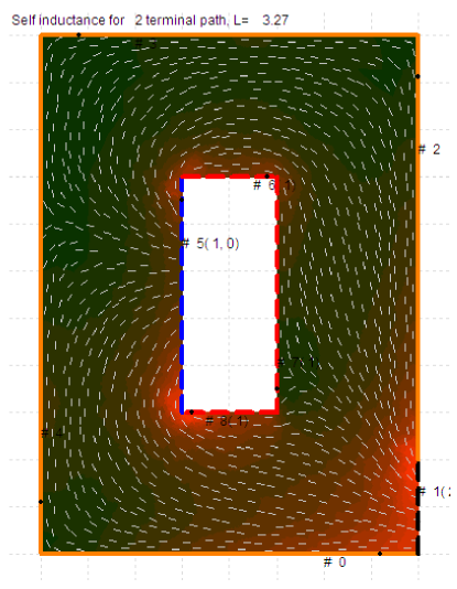
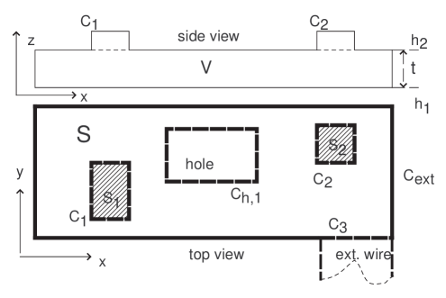
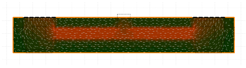
Consider simple inductances calculations demonstrating the model of hole as terminal. The structure we consider is plate with thickness and with hole and London penetration depth . On Fig. 2 current density and current direction with small vanes are shown. When we calculate the inductances we set full currents around holes and full currents flowing across terminals as . For hole it means that some fluxoid is trapped in the hole where is the inductance of hole.
Fig. 2a show currents for self inductance of the hole. Simple estimation using per-unit-length inductances of coplanar lines of width and and spacing between lines gives . In this estimation we calculate per-unit-length inductances using 2D program Khapaev, (1996). These inductances are for spacing and for spacing . We take length of strips and to account corners of the hole. Our result with 3D-MLSI is and match estimation well.
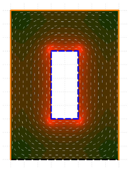
Fig. 2b demonstrates results for hole as terminal. All four sides of the hole inject current with uniform density. Current leave plate across bottom boundary. Inductance of this current path is .
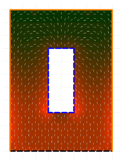
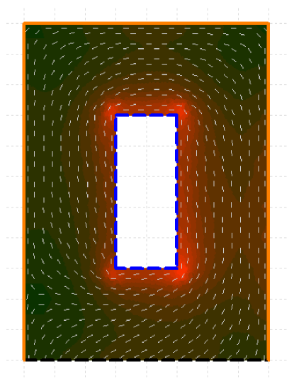
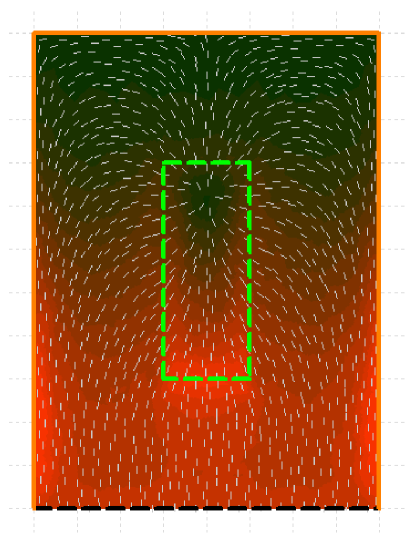
Also, we can calculate mutual inductance of current circulating around the hole and current from hole to bottom side. This inductance is very small (pH ) because the problem is symmetric. Spatial distribution of the current is shown in Fig. 3a.
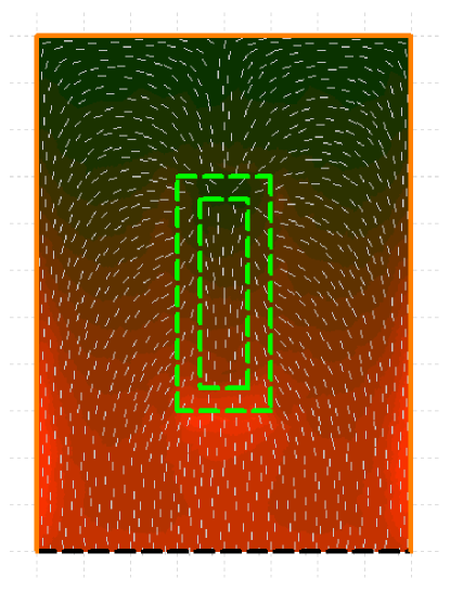
We can consider only one side of hole as a terminal. Other terminal is part of right border of the plate. The current distribution for this case is shown in Fig. 3b. The inductance of this current path is . Mutual inductance between current around hole and terminal to terminal current path is .
V.2 Hole as current source
Next calculations are performed for model of hole as current source. In this case, area of contact isn’t cutted out and there are no hole in the film but current source with homogenous density is present. We consider the same plate with area of current source.
Current directions are shown in Fig. 4a, the inductance of this current path is .
The current source can be more complicated. On Fig. 4b we demonstrate coil-like source simulating London current crowding effect in the vertical contact. The inductance in this case is .
V.3 Multilayer interferometer
The next example is multilayer interferometer designed for IPHT RSFQ process Fourie et al., (2013). Design contains three layers, , and thick and The distances between the layers are and . The shape and dimensions of nets are presented in Fig. 5.
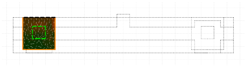
We consider a current circulating in all three layers. The first layer is the ground plane, see Fig. 5b. The second layer consists of two square parts, see Fig. 5c. The parts are symmetric so only left part is shown on Fig. 5c. Ground plane is connected with second layer by two contacts shown on Fig. 5b and Fig. 5c by dashed segments. The second layer, see Fig. 5c, is connected with the third layer using the square current source terminals shown on Fig. 5c, Fig. 5d by dashed squares.
It is assumed that a uniformly distributed supercurrent is injected into the second layer through the dashed segment located in the left part of the second layer. Then it flows across the left rectangle to square dashed current source and jump to the third layer. For third layer inlet current source is left dashed square and outlet source is right dashed square. Then current symmetrically returns back across right part of second layer. First layer carry all return current.
We calculate inductance for this closed current loop. It is . The inductance of strip of length in third layer over groundplane is .
In Fig. 5a mesh of triangles is shown. This mesh is created for all nets once taking into account all projections on bottom layer plane. In this case, the mesh accurately retrace all boundaries of nets. This adaptive non-regular mesh improves accuracy of FEM.
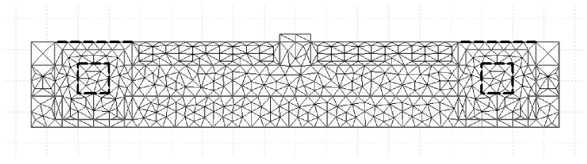
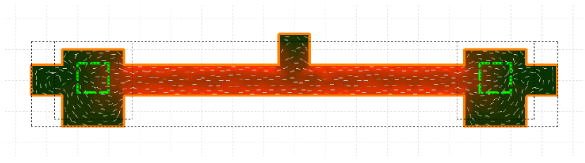
a) The result of layout meshing using program ”Triangle”. b) Spatial distribution of supercurrent in the groundplane (first metal layer). Groundplane length is , width is . c) Spatial distribution of supercurrent in left net in second layer. Squared dashed internal contact is d) Spatial distribution of supercurrent in third layer (metal 3). Width of strip part is , length is .
VI Conclusions
We developed the new version of 3D-MLSI software for calculation of inductances and currents in complex multilayer superconductor structures. It provides higher accuracy and computing performance. We have now the simulation tool that allow calculation of inductances, currents and fields of practically all superconductor structures. We significantly improve the numerical algorithm of 3D-MLSI software. To do this we further developed the meshing procedure by using well recognized triangulation engine tool ”Triangle” as the core of meshing. Moreover we implemented triangulation for joint projection of all nets thus improving discrete physical model for inductance extraction in layouts designed for planarized and non-planarized fabrication processes. We introduced two physical model for description of the internal terminals that are staggered or stacked vias between layers or connections between the films contained Josephson junction. Using simple examples, we have demonstrated their ability to describe the spatial distribution of the currents and to calculate the inductances in structures and devices having contacts between the individual layers in multilayer designs.
We would like to thank V.K. Semenov, C.J. Fourie, E.B. Goldobin and L.R. Tagirov for fruitful discussions and C.J. Fourie for practical testcase. M.K. acknowledge partial support by the Program of Competitive Growth of Kazan Federal University.
References
References
- IAR, (2014) (2014). Cryogenic computing complexity (C3): http://www.iarpa.gov/index.php/research-programs/c3.
- Anders et al., (2010) Anders, S., Blamire, M., Buchholz, F.-I., Crété, D.-G., Cristiano, R., Febvre, P., Fritzsch, L., Herr, A., Il’Ichev, E., Kohlmann, J., Kunert, J., Meyer, H.-G., Niemeyer, J., Ortlepp, T., Rogalla, H., Schurig, T., Siegel, M., Stolz, R., Tarte, E., Ter Brake, H., Toepfer, H., Villegier, J.-C., Zagoskin, A., and Zorin, A. (2010). European roadmap on superconductive electronics - status and perspectives. Physica C: Superconductivity and its Applications, 470(23-24):2079–2126.
- Bunyk and Rylov, (1993) Bunyk, P. and Rylov, S. (1993). Automated calculation of mutual inductance matrices of multilayer superconductor integrated circuits. In Proc. Ext. Abstracts 4th Int. Supercond. Electron. Conf. (ISEC 93), Boulder, CO, page 62.
- Duzer and Turner, (1999) Duzer, T. V. and Turner, C. W. (1999). Principles of Superconductive Devices and Circuits, (Second Ed.). Prentice Hall PTR, Upper Saddle River, NJ, USA.
- Fourie, (2013) Fourie, C. (2013). Calibration of inductance calculations to measurement data for superconductive integrated circuit processes. Applied Superconductivity, IEEE Transactions on, 23(3):1301305–1301305.
- Fourie and Volkmann, (2013) Fourie, C. and Volkmann, M. (2013). Status of superconductor electronic circuit design software. Applied Superconductivity, IEEE Transactions on, 23(3):1300205–1300205.
- Fourie et al., (2013) Fourie, C., Wetzstein, O., Kunert, J., Toepfer, H., and Meyer, H.-G. (2013). Experimentally verified inductance extraction and parameter study for superconductive integrated circuit wires crossing ground plane holes. Superconductor Science and Technology, 26(1):015016.
- Fourie et al., (2011) Fourie, C., Wetzstein, O., Ortlepp, T., and Kunert, J. (2011). Three-dimensional multi-terminal superconductive integrated circuit inductance extraction. Superconductor Science and Technology, 24(12):125015.
- Fourier, (2014) Fourier, C. (2014). Inductex version 4.26. online: http://stbweb02.stb.sun.ac.za/inductex/.
- Fujimaki et al., (2014) Fujimaki, A., Tanaka, M., Kasagi, R., Takagi, K., Okada, M., Hayakawa, Y., Takata, K., Akaike, H., Yoshikawa, N., Nagasawa, S., Takagi, K., and Takagi, N. (2014). Large-scale integrated circuit design based on a Nb nine-layer structure for reconfigurable data-path processors. IEICE Transactions on Electronics, E97-C(3):157–165.
- Gaj et al., (1999) Gaj, K., Herr, Q., Adler, V., Krasniewski, A., Friedman, E., and Feldman, M. (1999). Tools for the computer-aided design of multigigahertz superconducting digital circuits. Applied Superconductivity, IEEE Transactions on, 9(1):18–38.
- Jin, (2002) Jin, J. (2002). The Finite Element Method in Electromagnetics. A Wiley-Interscience publication. Wiley.
- Kamon M. and J.K., (1994) Kamon M., T. M. and J.K., W. (1994). Fasthenry: a multipole-accelerated 3-D inductance extraction program. Microwave Theory and Techniques, IEEE Transactions on, 42(9):1750–1758.
- Khapaev, (1996) Khapaev, M. (1996). Extraction of inductances of a multi-superconductor transmission line. Superconductor Science and Technology, 9(9):729–733.
- Khapaev, (2001) Khapaev, M. (2001). Inductance extraction of multilayer finite-thickness superconductor circuits. Microwave Theory and Techniques, IEEE Transactions on, 49(1):217–220.
- Khapaev et al., (2001) Khapaev, M., Kidiyarova-Shevchenko, A., Magnelind, P., and Kupriyanov, M. (2001). 3D-MLSI: software package for inductance calculation in multilayer superconducting integrated circuits. Applied Superconductivity, IEEE Transactions on, 11(1):1090–1093.
- (17) Khapaev, M. and Kupriyanov, M. (2010a). Sheet current model for inductances extraction and josephson junctions devices simulation. Journal of Physics: Conference Series, 248:012037(1)–012037(8).
- (18) Khapaev, M. and Kupriyanov, M. (2010b). Sparse Approximation of FEM Matrix for Sheet Current Integro-Differential Equation, chapter 33, pages 510–522. World Scientific.
- Khapaev et al., (2003) Khapaev, M., Kupriyanov, M., Goldobin, E., and Siegel, M. (2003). Current distribution simulation for superconducting multi-layered structures. Superconductor Science and Technology, 16(1):24.
- Nagasawa et al., (2014) Nagasawa, S., Hinode, K., Satoh, T., Hidaka, M., Akaike, H., Fujimaki, A., Yoshikawa, N., Takagi, K., and Takagi, N. (2014). NB 9-layer fabrication process for superconducting large-scale SFQ circuits and its process evaluation. IEICE Transactions on Electronics, E97-C(3):132–140.
- Nagasawa et al., (2009) Nagasawa, S., Satoh, T., Hinode, K., Kitagawa, Y., Hidaka, M., Akaike, H., Fujimaki, A., Takagi, K., Takagi, N., and Yoshikawa, N. (2009). New Nb multi-layer fabrication process for large-scale SFQ circuits. Physica C: Superconductivity and its Applications, 469(15-20):1578–1584.
- Orlando and Delin, (1991) Orlando, T. and Delin, K. (1991). Foundations of Applied Superconductivity. Electrical Engineering Series. Addison-Wesley.
- Ren, (2003) Ren, Z. (2003). 2-D dual finite-element formulations for the fast extraction of circuit parameters in VLSI. Magnetics, IEEE Transactions on, 39(3):1590–1593.
- Rubinacci and Tamburrino, (2010) Rubinacci, G. and Tamburrino, A. (2010). Automatic treatment of multiply connected regions in integral formulations. Magnetics, IEEE Transactions on, 46(8):2791–2794.
- Ruehli, (1974) Ruehli, A. (1974). Equivalent circuit models for three-dimensional multiconductor systems. Microwave Theory and Techniques, IEEE Transactions on, 22(3):216–221.
- Shewchuk, (1996) Shewchuk, J. (1996). Triangle: Engineering a 2D Quality Mesh Generator and Delaunay Triangulator. In Lin, M. C. and Manocha, D., editors, Applied Computational Geometry: Towards Geometric Engineering, volume 1148 of Lecture Notes in Computer Science, pages 203–222. Springer-Verlag. From the First ACM Workshop on Applied Computational Geometry.
- (27) Tolpygo, S., Bolkhovsky, V., Weir, T., Johnson, L., Oliver, W., and Gouker, M. (2014a). Deep sub-micron stud-via technology for superconductor VLSI circuits. Journal of Physics: Conference Series, 507(PART 4).
- (28) Tolpygo, S., Bolkhovsky, V., Weir, T., Johnson, L., Oliver, W., and Gouker, M. (2014b). Deep sub-micron stud-via technology of superconductor VLSI circuits. Superconductor Science and Technology, 27(2).
- Tolpygo et al., (2014) Tolpygo, S. K., Bolkhovsky, V., Weir, T. J., Galbraith, C. J., Johnson, L. M., Gouker, M. A., and Semenov, V. K. (2014). Inductance of Circuit Structures for MIT LL Superconductor Electronics Fabrication Process with 8 Niobium Layers. ArXiv e-prints.
- Whiteley, (2014) Whiteley, S. R. (2014). Fasthenry 3.0wr: http://www.wrcad.com/ftp/pub/.