Sphynx: A Shared Instruction Cache Exporatory Study
Abstract
The Sphynx project was an exploratory study to discover what might be done to improve the heavy replication of instructions in independent instruction caches for a massively parallel machine where a single program is executing across all of the cores. While a machine with only many cores (fewer than 50) might not have any issues replicating the instructions for each core, as we approach the era where thousands of cores can be placed on one chip, the overhead of instruction replication may become unacceptably large. We believe that a large amount of sharing should be possible when the machine is configured for all of the threads to issue from the same set of instructions. We propose a technique that allows sharing an instruction cache among a number of independent processor cores to allow for inter-thread sharing and reuse of instruction memory. While we do not have test cases to demonstrate the potential magnitude of performance gains that could be achieved, the potential for sharing reduces the die area required for instruction storage on chip.
1 Introduction
Instruction caches are widely used to mediate the effects of reads from main memory, relative to computation time. The instruction cache is accessed for every instruction executed and program execution time can vary widely depending on the number of instruction cache misses [1]. In existing Graphics Processing Units (GPUs) and CPUs, each processor core has its own instruction cache. A unified or shared instruction cache that is used by many or all cores of a GPU or CPU has the potential to improve system performance and reduce power consumption. However, such a modification also results in increased traffic for the instruction cache, which could lead to a higher miss rate, reducing performance and increasing power consumption.
In current computer architectures, the instruction caches are independent of one another. However, since each processor uses the same set of instructions, it is plausible that a shared instruction cache could introduce non-trivial improvements in performance. Unified instruction caches could reduce the number of compulsory misses because an instruction previously executed by one streaming multiprocessor may be available for another streaming multiprocessor immediately rather than after an additional miss is serviced. In addition to a fully unified instruction cache used across all processor cores, another possible solution could be to maintain multiple instruction caches, which are shared across a subset of all cores. This architecture could allow the operating system to group together program threads based on similarity of instructions to maximize the benefit of shared instructions and minimize the conflicts across threads.
2 Background
An instruction cache can have a large impact in a processor’s performance. There has been lot of work in the past in improving the performance of instruction cache CPUs. Techniques such as advanced branch prediction [12] and replacement policies [7] have contributed to the high performance of instruction caches in modern CPUs. It has even been shown that system performance can increase by 10-20% just by adjusting the operating system to use the instruction cache efficiently [11]. While all of these approaches are useful, the future of computing includes very large numbers of independent processor cores integrated on one chip. While general purpose CPUs are likely to include hundreds of cores at some point in the future, a good example to consider today is the GPU, which already exposes hundreds to thousands of threads to the programmer.
Modern GPUs are designed to have several compute units to maximize throughput, and to expose these compute units for general purpose computation instead of only graphics applications. These compute units are compact, and designed to perform simple operations on a large set of data. It is not feasible to implement techniques such as advanced branch prediction on these small compute units, because a single GPU unit can have hundred of these compute units. To improve the instruction cache performance of GPUs, new solutions need to be developed in ways that maintain the compact and simplistic nature of the compute units. Current GPU architectures are designed with individual L1 instruction cache for each compute unit of the GPU[3]. It may be possible to have multiple compute units share the same instruction cache without incurring serious performance or power penalties.
3 Shared Instruction Cache Design

Most computer architectures build an independent instruction cache for each processing core as seen in Figure 1. Reducing the number of instruction caches for the same number of cores in a multi-core processor may have certain advantages. First, a shared instruction cache design could reduce the amount of storage and die area required to hold instructions on chip when multiple processors are executing the same program. This advantage in storage and area could result in reduced performance if the pressure to this shared resource becomes too high. Similarly, the benefits of reduced cache size will not be realized in multi-program workloads, unless the operating system is able to discover shared library code and perform the proper virtual mapping to allow the hardware to exploit it. Second, a shared instruction cache design could reduce the number of compulsory misses because an instruction previously fetched by one processor may be available for another processor immediately rather than requiring an additional cache miss. Again, this benefit is only relevant for single-application parallel workloads.

The first approach to shared instruction caches would be to couple an instruction cache with a pair of processors as in Figure 2. This would require a small amount of routing overhead and allow for the operating system or programmer to intelligently schedule two threads that share instructions to these two processor cores in order to exploit the shared instruction cache. While sharing an instruction between two cores is one step towards shared caches, at its limit, a chip could be designed to share a single instruction cache among all processors on chip, shown with an example of only four processors in Figure 3. For an arbitrary number of cores, the level of sharing could be scaled up or down to fit the applications and purpose of the architecture design. One could even imagine a design where assymetrical sharing is enabled by grouping different sets of compute cores differently and then assigning the application threads to the appropriate cores to match the sharing to the hardware available.
While our proposed technique is likely only beneficial in situations with highly parallel programs, it is probable that future systems will often run a few highly parallel workloads that can benefit from these advantages. A hybrid approach would allow some cores to efficiently process general purpose applications while cores with shared instruction caches execute parallel single program workloads. When different threads within a parallel application diverge in program flow, it may be useful to further design the instruction caches to have multiple independent banks that can be accessed in parallel. We believe the multi-banked approach to be the most beneficial, however we do not present results or analysis of multi-banked caches in this work.

4 Results
There are two methods for analyzing the potential gains from shared instruction caches. The first is to keep the total instruction cache size across the chip constant and increase the capacity each thread sees by grouping that storage together. This method of sharing will provide no area savings, but should grant an increased hit rate for the now larger cache. The increase will be limited by the working set of the application. We expect that the hit rate improvement will only be minor and therefore do not generate any results for this method.
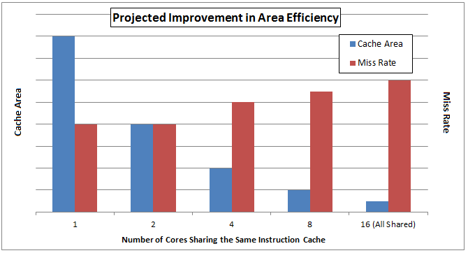
The second method is to reduce the total storage required for instruction cache data arrays while allowing at most a minor degredation in hit rate. We consider an approach where the instruction cache each processor sees remains fixed but the number of threads sharing each cache is increased. We expect that the miss rate of the cache will increase when the instruction cache is not large enough to satisfy the demands from all the cores sharing the cache. However, the performance penalty should not be as dramatic as the reduction in area when all threads run the same application. Figure 4 shows our hypothesis for this approach which should improve the efficiency of the chip. Note that the scale on the y-axis is omitted because the chart is included to build intuition of the hypothesis only and is not based on any simulation or otherwise realistic result.

4.1 Setup
We use GPGPU-Sim [2] to analyze the effectiveness of our design because of its ability to simulate a large number of parallel processing cores. GPGPU-Sim is an open-source software package available to simulate GPU architecture. It has been validated to be representative of performance on NVIDIA GPUs and provides a reasonable platform for testing alternate highly-parallel computer architectures. We use a reference configuration for a NVIDIA GTX580 GPU for our study. The GTX580 contains 16 streaming multiprocessors (SM) with the NVIDIA Fermi architecture. In GPGPU-Sim, each CUDA streaming multiprocessor is represented as a single SIMT core, with all the SIMT cores placed within a single SIMT cluster. Each streaming multiprocressor can have up to 48 warps, with 32 threads per warp (See Table 1). All sixteen SIMT cores share unified 786KB L2 cache.
| SIMT cluster count | 1 / 2 / 4 / 8 / 16 |
|---|---|
| Cores per cluster | 1 |
| Memory controller count | 6 |
| Subpartition per mem. | 2 |
| Shader registers | 32768x(16 / 8 / 4 / 2 / 1 ) |
| Threads in pipeline | 1536x(16 / 8 / 4 / 2 / 1 ) |
| Threads per warp | 32 |
| Scheduler per core | 2x(16 / 8 / 4 / 2 / 1 ) |
| CTA per core | 8x(16 / 8 / 4 / 2 / 1 ) |
| Core clock | 700 MHz |
| L2 & Interconnect clock | 700 MHz |
| DRAM clock | 924 MHz |
| Topology | 13 / 14 / 16 / 20 / 28 |
| L1 Instruction Cache | 4 sets : 128B blocks : 4-way |
In the Fermi architecture, each streaming multiprocessor has its own distinct L1 cache. Each L1 instruction cache is 4-way set associative, with 4 sets of 128 bytes per block. To assess the performance of different L1 instruction cache architectures, only the L1 instruction cache was modified, while all other architectural variables remained constant. Other aspects of the architecture such as the bandwidth of shared L2 cache could serve as a performance bottleneck for different cache designs. However, these variables are ignored for this study, because we expect them to have little impact on the hit and stall rates of the instruction cache, which are the primary metrics of interest.
4.2 Preliminary Results
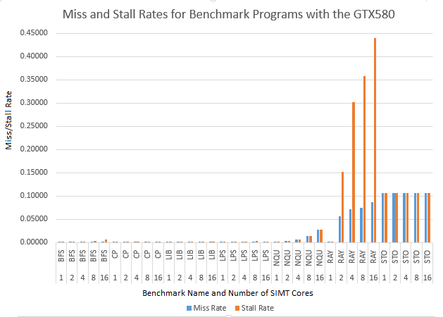
We used benchmarks provided by the standard GPGPU-Sim distribution to validate our second method for sharing instruction caches by keeping the cache the same but increasing the number of threads that share that cache. This means varying the number of SMs per instruction cache from 1 to 16 (the maximum number of cores available on the GTX580). Note that since each SM can have up to 48 warps, the number of simultaneously executing threads sharing the same instruction cache is much larger than the SM count. The results can be seen in Figures 5 and 6. As expected, the miss rate increases slightly in most cases by the increased pressure on the shared cache. A couple of benchmarks were more problematic, resulting in almost a 45% stall rate when shared by 16 threads. We provide observations about those benchmarks in Section 4.3.

For the cases where the miss rate becomes unacceptable under increased sharing, we should allow for the cache to increase in capacity. However, capacity alone will only affect the miss rate reported from the simulations. The stall rate represents the percentage of cache accesses that fail due to the increased pressure on the cache from sharing without increasing the available read parallelism. We expect that simply allowing for independent banks of the instruction cache to be accessed independently would overcome this limitation, but we have not yet simulated this approach. However, other high-level simulation has shown this kind of instruction cache banking scheme to be potentially effective [6].
4.3 Benchmarks
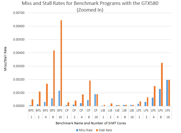
The result of varying the number of SM sharing from 1 to 16 is shown in Figure 5, and Figure 6 shows a zoomed-in version of the same data to show that even when the magnitude of misses is very small, the expected trend is followed. A total of seven benchmarks were tested, each available from the GPGPU-Sim source code [2].
The benchmark STO is mostly unaffected by the increase in number of cores accessing the same small instruction cache, and the benchmark shows a similar level of miss and stall rate. On the other hand, RAY exhibits a much higher stall rate than its miss rates in Figure 5, and is evidently more sensitive to increased sharing of the cache. Higher stall rate compared to miss rate occurs when the cache is not able to respond to the CPU on time, even when there is a cache hit. The rapid increase in stall rate in RAY and the relatively modest increase in miss rate suggests the cache is not able to handle the rapid increase in the amount of requests coming from the cores, and has to stall even when there is a hit.
As RAY showed to have the largest number of PTX instructions amongst our set of benchmarks, the high miss and stall rate is reflective of the high level of instruction cache utilization by the benchmark.
Similar relationships between stall rate and miss rate are also evident in benchmarks BFS, CP, and LPS. However, the miss rate of less than 1% in these benchmarks suggests that the benchmarks are largely affected by initial compulsary misses, and operate largely on a small set of instructions.

5 Conclusions
The proposed instruction cache designs provide a possible solution to increase the efficiency of instruction cache in parallel processors, in particular processors whose primary workload includes single programs with many parallel threads executing the same code. The sharing of instruction cache amongst multiple cores can help chip designers optimize for less area without compromising performance. The extra space recovered from the sharing of instruction cache among multiple cores can be repurposed to improve other parts of the chip, such as a larger data cache(s) or additional computation units. We showed results for GPU workloads because they typically exhibit much higher levels of parallelism than CPUs while still executing a single application. GPUs traditionally only expose multi-program workload capabilities using corse-grained time-sharing among processes.
For future work, the proposed instruction cache design should be simulated and tested to verify the affectiveness of the design. The different cache architecture parameters that are expected to affect the performance of instruction cache design are: number of cores sharing the cache, associativity and size of the cache. Extensive testing of such parameters should be conducted to determine the most optimal instruction cache design for common workloads. The proposed design is expected to perform the best on multi-threaded applications with a large amount of redundant instructions, so the drawbacks of running non-redundant code should also be considered.
Acknowledgement
We acknowledge that this idea for reducing the instruction cache area overhead by aggressively sharing the cache originally came from previous work on the TRaX architecture [9, 8, 6, 10, 4, 5]. The TRaX architecture was designed for ray tracing and supports thousands of threads running the same application but working on different data. We would also like to acknowledge the reviews from Konstantin Shkurko and Steven Jacobs. This work was completed at Harvey Mudd College in Claremont, California.
bstctl:etal, bstctl:nodash, bstctl:simpurl
References
- [1] R. Arnold et al., “Bounding worst-case instruction cache performance,” in In IEEE Real-Time Systems Symposium, 1994, pp. 172–181.
- [2] A. Bakhoda et al., “Analyzing cuda workloads using a detailed gpu simulator,” in IEEE International Symposium on Performance Analysis of Systems and Software (ISPASS), 2009.
- [3] S. W. Keckler et al., “Gpus and the future of parallel computing,” IEEE Micro, vol. 31, no. 5, pp. 7–17, 2011.
- [4] D. Kopta et al., “An energy and bandwidth efficient ray tracing architecture,” in High-Performance Graphics (HPG 2013), 2013.
- [5] D. Kopta et al., “Memory considerations for low energy ray tracing,” in Computer Graphics Forum, 2014.
- [6] D. Kopta et al., “Efficient MIMD architectures for high-performance ray tracing,” in IEEE International Conference on Computer Design (ICCD), 2010.
- [7] J. Smith and J. Goodman, “Instruction cache replacement policies and organizations,” Computers, IEEE Transactions on, vol. C-34, no. 3, pp. 234–241, March 1985.
- [8] J. Spjut et al., “TRaX: A multicore hardware architecture for real-time ray tracing,” IEEE Transactions on Computer-Aided Design, vol. 28, no. 12, pp. 1802 – 1815, 2009.
- [9] J. Spjut et al., “TRaX: A multi-threaded architecture for real-time ray tracing,” in 6th IEEE Symposium on Application Specific Processors (SASP), June 2008.
- [10] J. Spjut et al., “A mobile accelerator architecture for ray tracing,” in 3rd Workshop on SoCs, Heterogeneous Architectures and Workloads (SHAW-3), 2012.
- [11] J. Torrellas, C. Xia, and R. L. Daigle, “Optimizing the instruction cache performance of the operating system,” Computers, IEEE Transactions on, vol. 47, no. 12, pp. 1363–1381, 1998.
- [12] T.-Y. Yeh, D. T. Marr, and Y. N. Patt, “Increasing the instruction fetch rate via multiple branch prediction and a branch address cache,” in Proceedings of the 7th international conference on Supercomputing. ACM, 1993, pp. 67–76.