Interplay between Raman shift and thermal expansion in graphene: temperature-dependent measurements and analysis of substrate corrections
Abstract
Measurements and calculations have shown significant disagreement regarding the sign and variations of the thermal expansion coefficient (TEC) of graphene . Here we report dedicated Raman scattering experiments conducted for graphene monolayers deposited on silicon nitride substrates and over the broad temperature range 150–900 K. The relation between those measurements for the G band and the graphene TEC, which involves correcting the measured signal for the mismatch contribution of the substrate, is analyzed based on various theoretical candidates for . Contrary to calculations in the quasiharmonic approximation, a many-body potential reparametrized for graphene correctly reproduces experimental data. These results indicate that the TEC is more likely to be positive above room temperature.
pacs:
65.80.Ck;68.65.Pq;63.22.Rc;65.40.deThe thermal expansion coefficient (TEC) of materials involved in solid interfaces is a key parameter characterizing the stress within the materials, which in turn can modulate its electronic properties.Ni08 The use of graphene in high density, integrated electronic devicesnovoselov04 ; zhang05 ; bolotin08 or as matrix reinforcement for composite materialsstankovitch06 would benefit from a better knowledge of the TEC, in particular its dependence on temperature .
Unfortunately, experiment and theory alike show markedly diverse results regarding the TEC of graphene. The scanning electronic microscopy (SEM) measurements carried by Bao et al. bao09 found negative values for at low temperature and a sign change at around 350 K. Similar conclusions were reached by Yoon et al.yoon11 who performed Raman scattering spectroscopy, although no sign change was observed below 400 K. Negative coefficients were also obtained by Singh et al. singh10 who used a nanoelectromechanical resonator. In both Refs. yoon11, and singh10, strong variations among samples were emphasized. On the theory side, density-functional perturbation theory (DFPT)mounet05 and ab initio molecular dynamics pozzo11 predicted an all negative in a broad temperature range, whereas non-equilibrium Green’s function calculationsjiang09 found a sign change near 600 K. Atomistic Monte Carlo (MC) simulations have found all positive, all negative or sign changing variations of the TEC depending on the potential used.zakharchenko11 ; magnin14 This diversity of behaviors is related to the importance of anharmonicitiesfasolino07 and the difficulty of describing them properly in relation with appropriate measurements.
Raman spectroscopy in a broad temperature range is one of the indirect ways to access such properties. Being a fast and non destructive tool that can offer structural and electronic informations, it has been widely used for the characterization of graphene.ferrari13 In particular, from such measurements the number of layers, density of defects, amount of stress and doping can all be evaluated.ferrari13 As a direct probe of the phonon structure, temperature-dependent measurements should be indirectly related to the lattice parameter, hence to the TEC. However, in experiments graphene is held on (or by) a substrate, and it is well known that the detailed graphene structure is sensitive to the nature of the support.soldano10 In particular, incommensurability between the two lattices gives rise to strain often manifested by corrugation,Preobrajenski08 and which could affect the measured TEC.jean13 More generally, the contact between the two materials having different thermal expansion coefficients is a source of strain.yoon11 Even though some authors have disregarded this correction in their measurements,bao09 the importance of substrate interactions on the TEC has been recognized before.jiang09
One limitation of earlier investigations is the rather restricted temperature ranges over which the measurements were conducted, generally below 400 K. In the present work, we have extended this range to an higher upper limit of 900 K. More importantly, we have carried out a comprehensive analysis of the Raman G band based on underlying models for the graphene TEC, carefully disentangling the contribution of the substrate by following the phenomenological procedure laid out by Yoon et al.yoon11 Our experimental results are found incompatible with TEC that remain negative in the entire temperature range, but agree reasonably well with an all-positive model TEC predicted by a dedicated atomistic potential precisely fitted to reproduce the phonon structure of graphene.
Strictly monolayer graphene was synthesized on a copper foil (25 m thick, 99.8% purity, AlfaAesar) by a pulsed CVD growth method.han13 After etching of the foil in a solution at mol/L concentration, the graphene sheet was directly transferred on a SiN membrane (thickness 50 nm) supported on a silicon substrate (Silson) using a resist-free technique.kim09 Before experiment, the samples were annealed in-situ at 600 K in an inert atmosphere. The measurements were carried out using two distinct Raman setups. First, a Renishaw RM 1000 micro-Raman spectrometer equipped with a 1800 lines/mm grating used a laser power kept low enough not to induce any shift of the G peak. A 50 long working distance objective was used, and the samples were heated and cooled in a Linkam THMSG600 in a ultra pure Ar (alphagaz 2, Air Liquide) atmosphere. A second homemade Raman setup was adapted to a ultrahigh vacuum (UHV) chamber (base pressure mbar) and a Horiba spectrometer (TRIAX320). The excitation wavelength was set to 532 nm in both experiments. The G and 2D peaks were fitted to single Lorentzians for analysis. Additional SEM imaging was performed after the Raman measurements in a FEI, NovaSEM 450 microscope at an acceleration voltage of 5 kV and with a sample tilted at 45° with respect to the electron beam.
In Fig. 1, panel (a) schematically depicts the graphene sample supported on the SiN/Si substrate, while panel (b) shows a SEM micrograph including the Raman laser spot. A typical Raman spectrum represented in the inset of Fig. 1(c) shows symmetric Lorentzian line shapes for the 2D peak and an intensity ratio with the G peak which are consistent with a single graphene layer.ferrari13 In addition, the low ratio with the D peak suggests a low density of defects.ferrari13
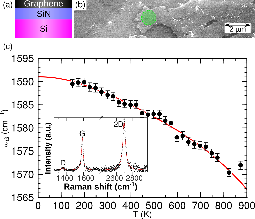
The variations of the G peak frequency with increasing temperature are shown as the main Fig. 1(c) for a sample in argon atmosphere. These reasonably smooth variations, together with the SEM data, indicate that the graphene layer does not present significant folded areas, cracks or wrinkles at least in the area probed by the laser. Additional measurements performed on other samples and under UHV or argon atmosphere show comparable results with a good reproducibility.SI
The room temperature value of found for our sample (1587.2 cm-1) is slightly shifted compared to the intrinsic value of 1581.6 cm-1 expected for charge- and strain-free graphene,lee12 suggesting mild amounts of defects in our sample. The small discontinuities of 1–2 cm-1 observed for might originate from a stick-slip of the graphene layer on the nitride surface, as also visible on the measurements of Calizo and coworkers on silica substrates.calizo07 Between 100 and 400 K the temperature variations of are roughly linear with a slope of cm-1.K-1, in fair agreement with values reported previously for graphene deposited on silica substrates ( cm-1.K-1 in Ref. calizo07, , cm-1.K-1 in Ref. yoon11, ).
The observed thermal contribution to the Raman frequency shift of the G peak, , was evaluated by removing from the value extrapolated at 0 K using a polynomial fit, cm-1 (note that this fit serves no other purposes than extrapolating to the reference temperature). To determine the intrinsic Raman shift of the pure graphene layer, the contribution of the substrate-induced strain was removed from following the same procedure advocated by Yoon et al.yoon11 based on the TECs of both graphene and substrate,
| (1) |
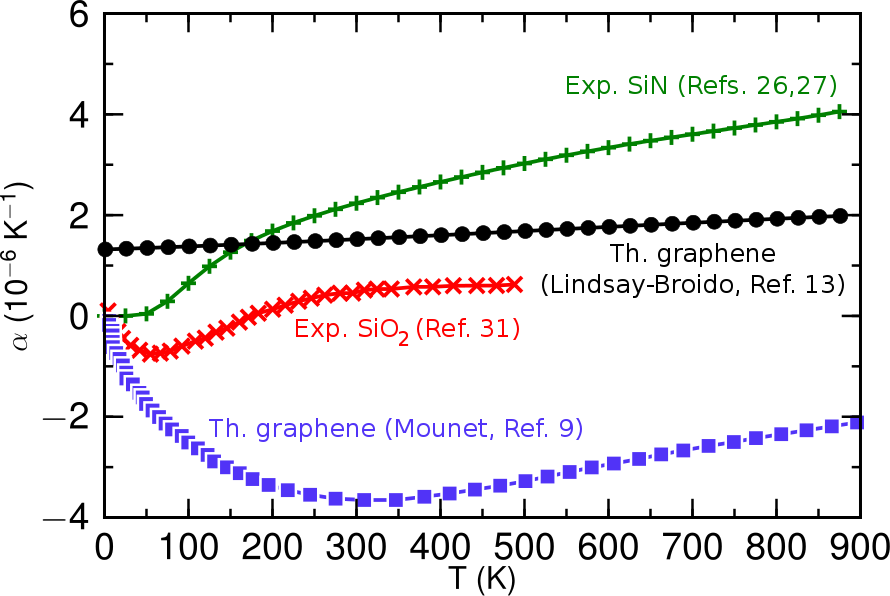
In the previous equation we have denoted by and the TECs of the substrate and of the graphene layer, respectively. is the biaxial strain coefficient of the G band known to be approximatelymohiuddin09 ; yoon11_2 cm-1/%. Eq. (1) is central to our analysis as it provides a relation between the experimentally measured Raman signal and the graphene TEC we aim to discuss. To evaluate the substrate contribution to the Raman signal it is necessary to integrate the thermal expansion coefficients of the two materials over temperature. The TEC of the SiN substrate was taken from the literaturesinha78 and extrapolated down to low temperatures K using data known for the similar Si3N4 system.si3n4
For graphene, several forms were tried for in the hope that comparison with experiment would ultimately settle generic conclusions about the expected features of this fundamental quantity. The DFPT results from Mounet and Marzarimounet05 were chosen as a representative of the quasiharmonic approximation based on first-principles data, giving a TEC that we denote as and that is entirely negative in the relevant temperature range. Alternatively, among the various predictions of fully anharmonic MC simulations based on atomistic potentialsmagnin14 we have chosen those obtained with a recent reparametrization of the Tersoff bond-order potentialtersoff by Lindsay and Broidolindsay10 dedicated to graphene, . The variations of the three aforementioned thermal expansion coefficients with temperature are represented in Fig. 2.
The strong discrepancies between the two model TECs for graphene are expected to convey to the Raman shift, and we have reported in Fig. 3 the variations of obtained by integrating Eq. (1) with the corresponding functions or .
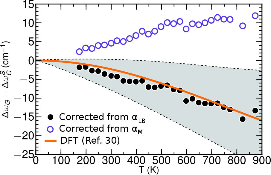
In order to compare the relative performances of the two models, a third set of reference data is required, which is provided by the theoretical Raman shift of freestanding graphene calculated by Bonini and coworkersbonini07 using density-functional theory (DFT) calculations under appropriate anharmonic expansions. This purely theoretical result, depicted also in Fig. 3 clearly agrees quantitatively with the present measurements if the substrate correction originates from the Lindsay-Broido model, but disagrees otherwise. It is important to evaluate the sensitivity of this result to the ingredient, and we have repeated the integration using the model but shifting it by K-1 in the entire temperature range, a negative shift leading to a positive TEC at low temperature and a sign change near 400 K. The resulting Raman shift of the G band also varies (see Fig. 3) but remains closer to the reference DFT data than the values obtained with the correction. This observation puts some constraints on the true function.
According to the present measurements and analysis, the graphene TEC is better described by the Lindsay-Broido model than the Mounet-Marzari quasiharmonic model. It is tempting to challenge those conclusions by considering the case of silica substrates, on which earlier Raman measurements have been performed.yoon11 ; calizo07 Two sets of experimental data were borrowed from the works of Yoon and coworkersyoon11 and Calizo et al.,calizo07 respectively, and subject to the same correcting treatment as performed here for silicon nitride but using the experimental thermal expansion coefficient of silicasio2 also superimposed in Fig. 2. From these two data sets for , the correction was calculated from the two graphene model TECs and , and the results are again compared to the reference DFT results of Bonini and coworkersbonini07 in Fig. 4.
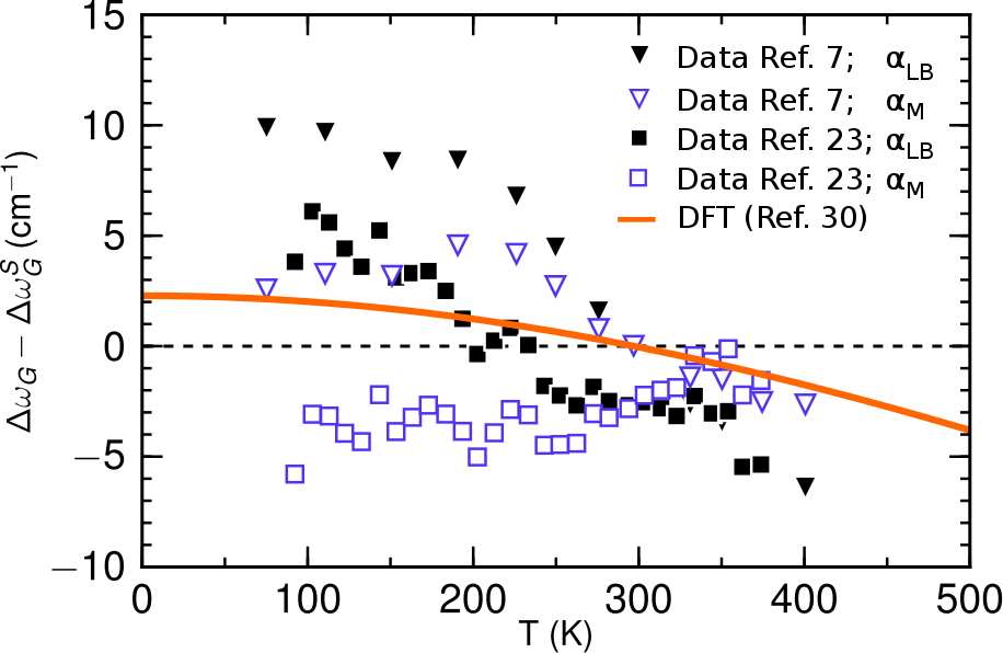
Correcting the data by Yoon et al. with the Mounet-Marzari model for leads to values for the Raman shift that are in good agreement with those obtained in Ref. yoon11, , as expected. They are significantly closer to the DFT reference data than those obtained with the all-positive TEC predicted by the Lindsay-Broido model, although the agreement is never excellent. Incidentally we note that Yoon and coworkers had to significantly adjust the input in order to get an even better agreement. However, the opposite observations can be made when the calculations are performed using the experimental data from Calizo et al.,calizo07 and a fully negative model for markedly underestimates the Raman shift while the Lindsay-Broido model yields reasonable agreement. Given the significant dispersion among experimental measurements for graphene on SiO2 substrates,yoon11 ; calizo07 and in particular the much more limited temperature range on which these measurements have been conducted, it seems difficult to conclude unambiguously based on the silica data alone whereas the present data obtained on silicon nitride display better overall agreement with theoretical models.
The discrepancies between the predictions of the Mounet-Marzari and Lindsay-Broido corrections are related to the rather different nature of the two models, the former quasiharmonic modelmounet05 being expected to be better at low temperature while the latter, anharmonic but classical modellindsay10 was adjusted on room temperature properties. Both models were not fitted to reproduce temperature-dependent properties, hence it is also unclear to which extent they would be able to correctly capture anharmonicities especially above room temperature. In absence of independent measurements, and in view of the major diversity among computational models,magnin14 it is tempting to conclude that the true thermal expansion coefficient lies somewhere inbetween the two models, hence that it must at least be positive above some temperature close to 300 K.
In summary, we have performed Raman scattering measurements of graphene monolayers supported on silicon nitride over an extended temperature range, and used these data to establish some constraints on the TEC of pure graphene. Our analysis relies on the correction to the measured Raman shift of the G band due to the mismatch contribution from the substrate, and on the comparison of the corrected signal to benchmark anharmonic DFT calculations.bonini07 The present approach, which follows earlier efforts by other authors,yoon11 requires knowledge of the expansion coefficients of both graphene and substrate materials. A model TEC based on finite temperature MC simulations with a potential dedicated to graphene turned out to reproduce best the experimental data, suggesting that the TEC is more likely to be positive above moderate temperatures. Until more direct measurements are carried out, one main outcome of the present work is the confirmation that the substrate plays a great role on the thermal properties of graphene,jiang09 and this contribution should not be neglected in general especially when attempting some theoretical predictions. Future work could be devoted to extending the present methodology to other 2D or layered materials such as hexagonal boron nitride or to transition metal dichalcogenides that currently hold promises for their interesting semiconductor properties.wang12
The authors gratefully acknowledge the CECOMO (Univ. Lyon 1) for providing access to the Raman spectroscopy facilities and C. Albin (ILM, PLYRA). Research supported by ANR Contract No. ANR-2010-BLAN-1019-NMGEM.
References
- (1) Z. H. Ni, T. Yu, Y. H. Lu, Y. Y. Wang, Y. P. Feng and Z. X. Shen, ACS Nano 2, 2301 (2008).
- (2) K. S. Novoselov, A. K. Geim, S. V. Morozov, D. Jiang, Y. Zhang, S. V. Dubonos, I. V. Grigorieva and A. A. Firsov, Science 306, 666 (2004).
- (3) Y. Zhang, Y.-W. Tan, H. L. Stormer and P. Kim, Nature (London) 438, 201 (2005).
- (4) K. I. Bolotin, K. J. Sikes, Z. Jiang, M. Klima, G. Fudenberg, J. Hone, P. Kim and H. L. Stormer, Solid State Commu. 146, 351 (2008).
- (5) S. Stankovich, D. A. Dikin, G. H. B. Dommett, K. M. Kohlhaas, E. J. Zimney, E. A. Stach, R. D. Piner, S. T. Nguyen and R. S. Ruoff, Nature (London) 442, 282 (2006).
- (6) W. Bao, F. Miao, Z. Chen, H. Zhang, W. Jang, C. Dames and C. N. Lau, Nat. Nanotech. 4, 562 (2009).
- (7) D. Yoon, Y.-W. Son and H. Cheong, Nano Lett. 11 3227 (2011).
- (8) V. Singh, S. Sengupta, H. S. Solanki, R. Dhall, A. Allain, S. Dhara, P. Pant and M. M. Deshmukh, Nanotechnology 21, 165204 (2010).
- (9) N. Mounet and N. Marzari, Phys. Rev. B 71, 205214 (2005).
- (10) J. W. Jiang, J. S. Wang and B. Li, Phys. Rev. B 80, 205429 (2009).
- (11) M. Pozzo, D. Alfè, P. Lacovig, P. Hofmann, S. Lizzit and A. Baraldi, Phys. Rev. Lett. 106, 135501 (2011).
- (12) K. V. Zakharchenko, A. Fasolino, J. H. Los and M. I. Katsnelson, J. Phys.: Cond. Matt. 23, 202202 (2011).
- (13) Y. Magnin, G. D. Förster, F. Rabilloud, F. Calvo, A. Zappelli and C. Bichara, J. Phys.: Cond. Matt. 26, 185401 (2014).
- (14) A. Fasolino, Nat. Mater. 6, 858 (2007).
- (15) A. C. Ferrari and D. M. Basko, Nat. Nanotech. 8, 235 (2013).
- (16) C. Soldano, A. Mahmood, and E. Dujardin, Carbon 48, 2127 (2010).
- (17) A. B. Preobrajenski, M. L. Ng, A. S. Vinogradov and N. Martensson, Phys. Rev. B 78, 073401 (2008).
- (18) F. Jean, T. Zhou, N. Blanc, R. Felici, J. Coraux and G. Renaud, Phys. Rev. B 88, 165406 (2013).
- (19) Z. Han, A. Kimouche, D. Kalita, A. Allain, H. Arjmandi-Tash, A. Reserbat-Plantey, L. Marty, S. Pairis, V. Reita, N. Bendiab, J. Coraux, and V. Bouchiat, Adv. Funct. Mater. 24, 964 (2014).
- (20) K. S. Kim, Y. Zhao, H. Jang, S. Y. Lee, J. M. Kim, K. S. Kim, J.-H. Ahn, P. Kim, J.-Y. Choi and B.H. Hong, Nature (London) 457, 706 (2009).
- (21) See Supplemental Material at http://link.aps.org/supplemental/DOI for additional Raman spectroscopy measurements
- (22) J. E. Lee, G. Ahn, J. Shim, Y. S. Lee, and S. Ryu, Nat. Commun. 3, 1024 (2012).
- (23) I. Calizo, A. A. Balandin, W. Bao, F. Miao and C. N. Lau, Nano Lett. 7, 2645 (2007).
- (24) T. M. G. Mohiuddin, A. Lombardo, R. R. Nair, A. Bonetti, G. Savini, R. Jalil, N. Bonini, D. M. Basko, C. Galiotis, N. Marzari, K. S. Novoselov, A. K. Geim and A. C. Ferrari, Phys. Rev. B 79, 205433 (2009).
- (25) D. Yoon, Y.-W. Son and H. Cheong, Phys. Rev. Lett. 106, 155502 (2011).
- (26) A. K. Sinha, H. J. Levinstein and T. E. Smith, J. Appl. Phys. 49, 2423 (1978).
- (27) W. Paszkowicz, R. Minikayev, P. Piszora, M. Knapp, C. Bähtz, J. M. Recio, M. Marqués, P. Mori-Sánchez, L. Gerward, and J. Z. Jiang, Phys. Rev. B 69, 052103 (2004).
- (28) J. Tersoff, Phys. Rev. B 37, 6991 (1988).
- (29) L. Lindsay and D. A. Broido, Phys. Rev. B 81, 205441 (2010).
- (30) N. Bonini, M. Lazzeri, N. Marzari and F. Mauri, Phys. Rev. Lett. 99, 176802 (2007).
- (31) Standard Reference Material 739 Certificate; National Institute of Standards and Technology: Gaithersburg, MD, 1991.
- (32) Q. H. Wang, K. Kalantar-Zadeh, A. Kis, J. N. Coleman and M. S. Strano, Nat. Nanotech. 7, 699 (2012).