Effects of Coulomb screening and disorder on artificial graphene based on nanopatterned semiconductor
Abstract
A residual disorder in the gate system is the main problem on the way to create artificial graphene based on two-dimensional electron gas. The disorder can be significantly screened/reduced due to the many-body effects. To analyse the screening/disorder problem we consider AlGaAs/GaAs/AlGaAs heterostructure with two metallic gates. We demonstrate that the design least susceptible to the disorder corresponds to the weak coupling regime (opposite to tight binding) which is realised via system of quantum anti-dots. The most relevant type of disorder is the area disorder which is a random variation of areas of quantum anti-dots. The area disorder results in formation of puddles. Other types of disorder, the position disorder and the shape disorder, are practically irrelevant. The formation/importance of puddles dramatically depends on parameters of the nanopatterned heterostructure. A variation of the parameters by 20–30% can change the relative amplitude of puddles by orders of magnitude. Based on this analysis we formulate criteria for the acceptable design of the heterostructure aimed at creation of the artificial graphene.
pacs:
73.21.-b, 73.21.FgI Introduction
Graphene is a carbon monolayer with a hexagonal honeycomb lattice. The material has a very special band structure described by the ultrarelativistic Dirac equation. Graphene has a number of exceptional properties that originate from the quantum and “relativistic” nature of the material. Discovery of this material in 2004 has had a profound impact on condensed-matter physics Novoselov07 ; CastroNeto09 and technology Novoselov12 . Electrons in graphene can travel for long distances without scattering, the electron mobility is 10 times larger than that in Si at room temperature. The major reason for the high mobility of electrons in graphene is the very high quality of the carbon lattice, there are very few defects in the lattice. An additional reason for the high mobility is the “ultrarelativistic” physics. It is well known that there is no backscattering for ultrarelativistic particles and this enhances the mobility.
The extraordinary properties of graphene originating from the particle dynamics in honeycomb/triangular lattice, have stimulated a number of researchers to realize quantum simulators of graphene in other systems. We broadly refer to this direction as artificial graphene. The major advantage of artificial graphene is in larger degree of control. These systems are tunable and therefore can be driven to complex topological/correlated phases which are not possible in natural graphene. Study of these phases is of fundamental importance and can lead to novel electronic applications such as the spin based transistor.
Recent advances have demonstrated the possibility of creating artificial graphene in diverse quantum systems. Current methods of design and synthesis include (i) nanopatterning of ultrahigh-mobility two-dimensional (2D) electron gases (2DEGs) Singha ; park09 ; Gibertini09 ; simoni10 ; Nadvornik12 ; Goswami12 , (ii) molecule-by-molecule assembly of honeycomb lattices on metal surfaces by scanning probe methods Gomes12 , (iii) trapping ultracold fermionic and bosonic atoms in honeycomb optical lattices Wunsch08 ; Soltan ; Tarruell12 ; Uehlinger , and (iv) confining photons in honeycomb photonic crystals haldane ; Bittner:2012 ; Rechtsman:2013 . For a review of the recent advances see Ref. polini13, .
It can be argued that whereas the molecular, atomic and photonic analogues of graphene offer a very high quality of the artificial lattice, the nanofabricated semiconductor analogue enables the exploration of the impact of long-range interactions, many-body effects, as well as the spin orbit interaction Sushkov13 . Technologically the semiconductor route to artificial graphene offers the key advantage of scalability as silicon and III-V materials are suitable for conventional top-down nanofabrication approaches. The realization of artificial graphene in semiconductors requires a fine control over disorder, whereas the other analogues of graphene are either disorder free (cold atoms on optical lattices) or characterized by tunneling energy scales that are substantially larger than disorder (molecules deposited on metals).
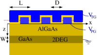
The residual disorder in heterostructure and in the gates system is the main problem on the way to create 2DEG artificial graphene suggested in Refs. Singha, ; park09, ; Gibertini09, ; simoni10, ; Nadvornik12, ; Goswami12, . In the present work we analyze the role of disorder and Coulomb screening in 2DEG artificial graphene. As a result of the analysis we formulate criteria for quality of quantum engineering necessary to create the artificial graphene. Lattices of anti-dots and quantum dots are investigated for more than 20 years, see Refs. Weiss1991, ; Baskin92, ; Dorn04, ; Gibertini09, ; mrres2012, ; Nadvornik12, and references therein, but observation of a miniband structure remains elusive. The main reason for that is a relatively poor quality of the created superlattice potential. The amplitude of uncontrolled random deviations of the potential from the perfect one are larger than the characteristic scale of the miniband structure. The honeycomb/triangular superlattice for artificial 2DEG graphene can consist of an array of quantum dots Gibertini09 or, alternatively, of an array of quantum anti-dots Nadvornik12 ; TkaTka14 . The present analysis indicates that the anti-dot structure is less sensitive to the superlattice disorder since the minibands are more dispersive. Therefore, here we pursue the “anti-dot” route. Usually systems of quantum dots and antidots are created in the 2DEG formed by doping. In simpler systems, such as quantum point contact, an alternative approach has been exercised, where the 2DEG and the nanosystem are patterned by two gates without doping. In this case the mobility of the low-density 2DEG is drastically increased due to the suppressed impurity scattering Pfeiffer ; Harrell ; pyshkin . Therefore, we consider an undoped AlGaAs/GaAs/AlGaAs heterostructure with two metallic gates. The lower metal gate laying on the surface of the semiconductor has perforation with period 100–130 nm, the gate is biased with a positive attracting voltage. A voltage on the top gate creates the anti-dots in the 2DEG beneath the holes perforated in the lower gate.
The paper is organized as follows. In Section II we consider an ideal device without any disorder in perforated gates. Even this problem is pretty involved technically due to the Coulomb screening in the gates and the self-screening in 2DEG. We find conditions for stability of the Dirac point, values of voltages which have to be applied to the gates, the miniband structure, the density of states, and the conductance of a finite size “sample”. In Section III we analyze disorder in the gates, in particular random deviations of sizes/positions/shapes of quantum anti-dots from the perfect structure. Here we calculate the density of states and the conductance of a finite size “sample”. Hence we determine the critical degree of disorder to preserve the Dirac physics. Our results and conclusions are summarized in Section IV.
II Ideal superlattice
II.1 Laterally patterned heterostructure
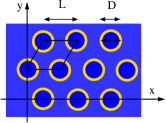
The laterally paterned heterostructure which we consider is shown in Fig. 1.
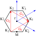
Brillouin zone of the triangular superlattice with lattice spacing is shown in Fig. 2. Wave vectors of the reciprocal lattice,
are also shown in Fig. 2. The points , , are connected by vectors , and are obtained from the by reflection.
Our convention is that corresponds to the bottom of the perforated gate, see Fig. 1. The electrostatic potential created by the gates, is a periodic function of which satisfies the Laplace equation, hence
| (1) |
At , close to the gates, the Fourier expansion has all harmonics. However, away from the gates, higher harmonics decay much faster than the first harmonic and hence in the 2DEG plane the potential created by gates is
| (2) | |||
Here is charge of the electron, corresponds to the location of 2DEG, and is the Bessel function. For the anti-dot array, which we consider, is positive. Negative corresponds to the array of dots.
II.2 Minibands in the noninteracting electron approximation
The miniband structure is determined by the Schrödinger equation
| (3) |
where is the effective mass and is due to the self-screening of 2DEG. In momentum representation the Schrödinger equation reads
| (4) |
First we disregard the self-screening and set . The band structure depends only on the dimensionless parameter
| (5) |
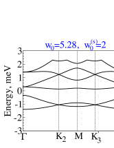
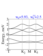
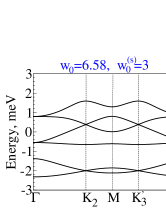
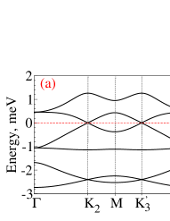
The Fourier component of (2), , is nonzero only if . Hence, truncating the summation in (4) by 20–50 states nearest in energy one reduces the problem to numerical diagonalization a matrix of about size. Six lowest calculated bands are shown in Fig. 3 for several values of .
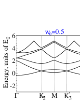
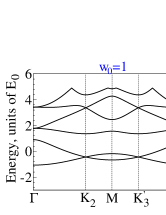
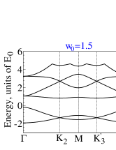
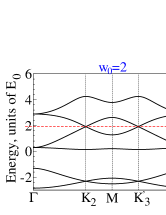
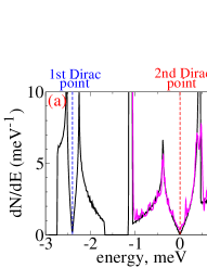
The first and the second Dirac points are well separated and clearly seen in panels (c) and (d) of Fig. 3. Higher Dirac points are “dissolved” in the dense band spectrum. Throughout the paper we will assume that the chemical potential is adjusted to the second Dirac point as it is shown in the panel (d) Fig. 3 by the red dashed line. The corresponding average electron density is .
II.3 Minibands in the Hartree approximation
The bands Fig. 3 are shown in dimensionless units. Below in this Section we set
| (6) | |||
Here we take . The average electron density corresponding to the second Dirac point is . For a usual 2DEG with quadratic dispersion and with dielectric constant this density corresponds to . The average density is pretty low. A local density is higher. We will discuss this issue later.
According to Fig. 3(d) the Fermi Dirac velocity is
| (7) |
Hence the “fine structure constant”
| (8) |
Here we take the dielectric constant . Hence, the interaction is stronger than that in natural suspended graphene where , see Ref. CastroNeto09, . To account for the 2DEG self-screening we use the Hartree approximation and solve Eq.(4) iteratively. We start from the noninteracting solution described in two previous paragraphs. Using this solution we calculate the electron density
| (9) |
Then we Fourier transform the density numerically, , and hence find
| (10) |
At the next iteration we substitute (10) in Eq. (4), find new wave functions and dispersions, calculate the electron density (9) and hence again calculate the screening potential (10). The iteration procedure converges after several iterations. When doing the iterations we keep the chemical potential adjusted to the second Dirac point, so we keep the average electron density unchanged. The self-screening potential has two effects. (i) partially screens the first harmonic in the gate potential (2), . (ii) generates higher harmonics in the effective potential. Six lowest bands calculated with account of screening are shown in Fig. 4 for several values of .
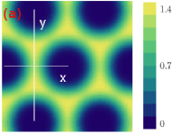
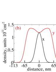
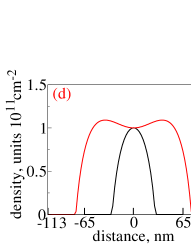
In the panels we present values of and also values of the screened constant . The spacial distribution of 2DEG electron density at parameters corresponding to Fig.4(d) is illustrated in Fig.5. Here we would like to stress two points; (i) The electron density, Fig.5(a), is connected, so this is the anti-dot regime, (ii) while the average electron density is , the density along the “connected manifold” is larger than . The value of the external potential modulation corresponding to Fig.4(d) is . Using Eqs.(2),(II.2),(6) we can find that the corresponding value of the gate voltages is ( nm, nm)
| (11) |
II.4 Minibands in the Poisson-Hartree approximation
The calculation described above has two inaccuracies, (i) Eq.(10) implies that the gate screening of the 2DEG self-screening (screening of screening) is not taken into account, (ii) we assume that the width of the 2DEG quantum well is very small . To fix these problems we perform an alternative, more involved and more accurate calculation of the miniband structure. We call this calculation the Poisson-Hartree calculation. We assume the following geometrical parameters, the lattice spacing nm, the perforation diameter nm, the distance from gates to 2DEG nm, the width of the rectangular quantum well nm. The wave function along the -direction is the lowest standing wave in the well, . Hence the total wave function is .
Instead of Eq. (9) the 2DEG electron density is
| (12) |
To find the electrostatic potential we solve Poisson equation, the gate voltages are imposed via boundary conditions at the metallic surfaces. With this potential we solve 2D Schrödinger Eq. (3), and find wave functions . Then we substitute this in Eq. (12) and iterate the procedure. This is the same Hartree procedure, but it accounts for finite and fully accounts for all screenings. Results of this calculation at V and V are presented in panels (a),(b), and (c) of Fig. 6. The gate voltages are adjusted to tune the chemical potential to the 2nd Dirac point, and to provide a sufficient modulation of the superlattice potential. The miniband structure Fig.6(a) and the electron density Fig.6(c) are pretty close to those obtained within the Hartree method and shown in Fig.4(d) and Fig.5. Fig.4(d) displays the situation close to the optimal one for the artificial graphene. We deliberately adjusted gate voltages to values
| (13) |
which approximately reproduce parameters corresponding to Fig. 4(d). The major difference between the result of the Hartree calculation and the result of the Poisson-Hartree calculation is the difference between Eq.(11) and Eq. (13). The Hartree method overestimates the value of because screening by gates is ignored in this consideration. As soon as is adjusted, all other results between the two methods are very close.
II.5 Minibands in the Poisson-Thomas-Fermi approximation
The analysis presented above is absolutely sufficient for an ideal superlattice. Unfortunately in a disordered system we cannot perform such an analysis because there is no band structure and there is no a well defined quasimomentum. Therefore, for a disordered system we will use the Poisson-Thomas-Fermi (Poisson-TF) method (see, for example, pyshkin, ; davies, ; modeling, ). Here we want to check how the method works for the perfectly periodic system. Idea of the method is very simple, instead of solving Schrödinger equation (3) and then using (9) to find the electron density, we use the local 2D Thomas-Fermi approximation to determine the density
| (14) |
Here is the effective chemical potential, and is the effective self-consistent potential. If expression in brackets in Eq.(14) is negative, we set . The effective chemical potential is determined by the equation
| (15) |
where the integration is performed over the lattice unit cell, and is the average electron density, for the second Dirac point. Using from Eq.(14) we solve the Poisson equation with appropriate boundary conditions at metallic gates, determine , and repeat the procedure iteratively. After completion of the iterative procedure we solve the Schrödinger equation, find the miniband structure, density of states, etc. By changing gate voltages we match the position of the second Dirac point to zero energy. The band structure and the density of states determined by this method are practically identical to that found within the Poisson-Hartree method and shown in panels (a),(b) of Fig. 6. The electron density, Fig. 6(d), is slightly different, though it is very close to the Poisson-Hartree density shown in panel (c). The main lesson we learn from this comparison is that we can rely on the Poisson-TF method for studies of disordered systems.
II.6 Recursive Green’s functions and conductance
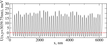
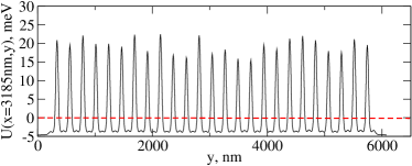
As soon as the effective potential is calculated by the Poisson-TF method we can calculate conductance of the artificial graphene “sample.” To do so we use the recursive Green’s function method Ando1991 ; Cresti2003 which is efficient for calculation of single particle pyshkin . We consider a “sample” of approximately size. In the -direction the size is limited by the width of the top gate. In the -direction the sample is connected to the metallic leads. The self-consistent potential plotted along the - and -directions is shown in Fig. 7.
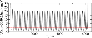
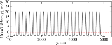
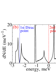
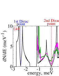
This is the case of M-orientation of anti-dot lattice with zigzag-configuration at the entries and with armchair-configuration along channel edges. Electric current flows in the -direction. To calculate Green’s functions we use effective potential interpolated on a coarse square grid (638574 sites) with 10 nm steps in - and -directions. The original , obtained within the Poisson-TF approach, is more detailed than the coarse grid we use for Green’s functions. We use the coarse grid since Green’s functions are computationally more intensive. The density of states calculated by the recursive Green’s function method is plotted in panel (a) of Fig.8 by the “noisy” magenta line.
The density of states is very close to that calculated from the band dispersion and shown by the solid black line in the same panel. The “noise” in the density of states calculated by the recursive Green’s function method is due to the finite size of the “sample.”
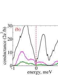
The calculated conductance is presented in panel (b) of Fig. 8.
Interestingly, at the Dirac point, , the conductance
does not dive to zero, .
We have checked that this is due to the two edge states located at nm
and nm. The edge states can be removed by a small
variation of the gate potentials (for example, there are no such states
at V,
V, in this case ).
The edge states are not topologically protected, therefore even a small
disorder will remove/influence the states.
Now we are fully armed to consider the effect of disorder
or in other words to consider an imperfect gate structure.
III Influence of disorder
III.1 Types of disorder
There are three different types of the gate disorder: (i) the area disorder, (ii) the position disorder, (iii) the shape disorder. In the case of the area disorder the radius of perforation, see Fig.1, is randomly changed
| (16) |
where is a random variable distributed uniformly in the interval . In this case the area of the perforated circle is randomly changed with the following rms variation
| (17) |
We assume that , therefore Eq. (16) is equivalent to a ring with random potential added to the regular gate potential
| (18) |
Here is the Dirac -function.
In the case of the position disorder the position of the perforation circle center is randomly changed
| (19) |
where is a unit vector with a random orientation in the plane. Again this is equivalent to a ring with random potential added to the regular gate potential
| (20) |
where is the angle between and .
In the case of the shape disorder the shape of the perforation circle is randomly changed, say circular to elliptic. This is also equivalent to a ring with the following random potential added to the regular gate potential
| (21) |
where is the angle between and the axis of the ellipse.
It is easy to check that 2D Fourier transforms of the disorder potentials (18),(20),(21) behave differently at small momenta, ,
| (22) |
The small components are the most important ones away from the gate plane since due to the Laplace equation they decay with as
| (23) |
From here we immediately conclude that assuming the effect of the area disorder is the most important one in the 2DEG plane. The effect of the position disorder on 2DEG is less important and the effect of the shape disorder is even smaller. We have checked this analytical conclusion by direct numerical simulations. Below we consider only the most dangerous area disorder.

III.2 Sensitivity to parameters and acceptable design
First we demonstrate dramatic sensitivity to parameters of the system. To do so, we do not solve selfconsistently Poisson-TF equations. Instead we just solve electrostatic Laplace equation. In doing so we keep in mind that the gate system must support artificial graphene. This implies that if we vary the lattice spacing the gate voltage must scale as , see Eq. (II.2), and, if vary the distance to 2DEG the gate voltage must scale as , see Eq. (2). In the panel (a) of Fig.9 we present map of the electrostatic potential of the perfect (no disorder) gate system with following parameters
| (24) |
The difference between minimum and maximum potential in this case is approximately 65 mV. In the panel (b) of Fig.9 we present map of the electrostatic potential for the gate system with the same parameters, but with some area disorder.
| (25) |
The rms area variation of the anti-dot, Eq. (17), is just 5%. Fig.9(b) clearly demonstrates the disorder induced puddles. The random variation of the potential is so strong that the range of the potential variation in panel (b) is almost four times larger than that in panel (a). So, in this case the gate disorder completely kills the miniband structure.
To reduce the relative effect of disorder we should decrease distance to the gates and increase the lattice spacing . In panel (a) of Fig.10 we present map of the electrostatic potential for the gate system with parameters similar to that of Fig.9(b). We just reduce and accordingly reduce .
| (26) |


Puddling in Fig.10(a) is significantly smaller than that in Fig.9(b), but still it is too strong. Finally in panel (b) of Fig.10 we present map of the electrostatic potential for the gate system with larger and accordingly reduced .
| (27) |
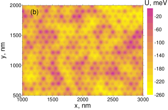
Puddling in Fig.10(b) is so small that it is not seen on the potential map.
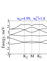
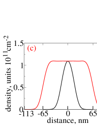
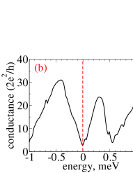
From Fig.10(b) one concludes that the parameter set (III.2) is acceptable. The maps Fig.9 and Fig.10 do not account for the 2DEG self screening. The 2DEG self screening taken into account via Poisson-TF method makes the potential fluctuation even smaller. Plots of the final self-consistent potential for a particular realization of the area disorder with parameter set (III.2) are presented in Fig.11. Note that leveling of the potential minimums in Fig.11 is much better than leveling of potential maximums. This is the effect of the charge density redistribution over the connected charged manifold, the “bright” net in Fig.5. Such screening is more efficient in the anti-dot geometry which we use. Leveling of the potential maximums is not as good since there are no electrons in vicinity of the maximums. The density of states and the conductance calculated with this self-consistent potential are shown in Fig.12(a),(b) by solid magenta lines. The density of states clearly demonstrates minimum near the second Dirac point, so the set of parameters (III.2) is acceptable for the artificial graphene design. On the other hand the dip in the conductance near the Dirac point is very weak. This is not surprising, the size of the “sample” is sufficiently large, and hence the electron dynamics becomes diffusive. This is the reason why the entire conductance curve lies significantly lower than that for the ideal sample (black solid line in Fig.12(b)). Obviously, the diffusive regime itself does not invalidate the Dirac physics.
We have also increased the disorder using the same parameter set (III.2) with only one change, nm nm. The increased corresponds to 10% rms variation of the anti-dot area, Eq.(17). The density of states and the conductance calculated in this situation are shown in Fig.12(a),(b) by solid green lines. The density of states minimum near the second Dirac point has almost gone, so this degree of disorder is the border-line for observation of the Dirac physics. Interestingly, even at this degree of disorder the band structure (allowed and forbidden energy bands) is still there and hence it can be observed in the density of states capacitance measurements Ponomarenko2010 .
IV Conclusions
We have analysed effects of the Coulomb many-body screening and effects of the residual disorder on the artificial graphene based on two-dimensional electron gas. Specifically we consider AlGaAs/GaAs/AlGaAs heterostructure with two metallic gates. The metallic gates make the many-body screening problem significantly different from that in natural graphene. We found that the design least susceptible to the disorder corresponds to the weak coupling regime (opposite to tight binding) which is realised via system of quantum anti-dots. The most dangerous type of disorder is the area disorder which is a random variation of areas of quantum anti-dots. The area disorder results in formation of puddles. Other types of disorder, the position disorder and the shape disorder, are practically irrelevant. The formation/importance of puddles dramatically depends on parameters of the nanopatterned heterostructure. For example a variation of the depth of the heterostructure by 30% (50 nm 37 nm) in combination with variation of the superlattice period by 30% (100 nm 130 nm) results in suppression of the relative amplitude of puddles by almost two orders of magnitude. Based on this analysis we formulate criteria for the acceptable design of the nanopatterned heterostructure aimed at creation of the artificial graphene.
Acknowledgements.
We thank A. R. Hamilton and O. Klochan for interest to the work and for numerous discussions. We also thank D. Baksheev for software optimizations. O. A. T. gratefully acknowledges the School of Physics at the University of New South Wales for warm hospitality during her visit. O. P. S. gratefully acknowledges Yukawa Institute for Theoretical Physics for warm hospitality during work on this project. This work was supported by Australian Research Council’s Discovery Project DP110102123. The work has been also supported by RAS (Russian Academy of Sciences) Presidium Program #24. The work has been also supported by SB RAS Integration Project #130. Computations were performed on RAS Joint Supercomputing Center MVS-10P (www.jscc.ru).References
- (1) Novoselov K S and Geim A K 2007 Nature Materials 6 183
- (2) Castro Neto A H, Guinea F, Peres N M R, Novoselov K S and Geim A K 2009 Rev. Mod. Phys. 81 109
- (3) Novoselov K S, Fal’ko V I, Colombo L, Gellert P R, Schwab M G and Kim K 2012 Nature 490 192
- (4) Singha A et al 2011 Science 332 1176
- (5) Park C H and Louie S G 2009 Nano Lett. 9 1793
- (6) Gibertini M, Singha A, Pellegrini V, Polini M, Vignale G, Pinczuk A, Pfeiffer L N and West K W 2009 Phys. Rev. B 79 241406(R)
- (7) Simoni G D, Singha A, Gibertini M, Karmakar B, Polini M, Piazza V, Pfeiffer L N, West K W, Beltram F and Pellegrini V 2010 Appl. Phys. Lett. 97 132113
- (8) Nadvornik L, Orlita M, Goncharuk N A, Smrcka L, Novak V, Jurka V, Hruska K, Vyborny Z, Wasilewski Z R, Potemski M and Vyborny K 2012 New J. Phys. 14 053002
- (9) Goswami S, Aamir M A, Siegert C, Pepper M, Farrer I, Ritchie D A and Ghosh A 2012 Phys. Rev. B 85 075427
- (10) Gomes K K, Mar W, Ko W, Guinea F and Manoharan H C 2012 Nature 483 306
- (11) Wunsch B, Guinea F, Sols F 2008 New J. Phys. 10 103027
- (12) Soltan-Panahi P, Struck J, Hauke P, Bick A, Plenkers W, Meineke G, Becker C, Windpassinger P, Lewenstein M and Sengstock K 2011 Nature Phys. 7 434
- (13) Tarruell L, Greif D, Uehlinger T, Jotzu G and Esslinger T 2012 Nature 483 302
- (14) Uehlinger T, Jotzu G, Messer M, Greif D, Hofstetter W, Bissbort U and Esslinger T 2013 Phys. Rev. Lett. 111 185307
- (15) Haldane F D M and Raghu S 2008 Phys. Rev. Lett. 100, 013904
- (16) Bittner S, Dietz B, Miski-Oglu M and Richter A 2012 Phys. Rev. B 85 064301
- (17) Rechtsman M C, Zeuner J M, Plotnik Y, Lumer Y, Podolsky D, Dreisow F, Nolte S, Segev M and Szameit A 2013 Nature 496, 196
- (18) Polini M, Guinea F, Lewenstein M, Manoharan H C and Vittorio Pellegrini V 2013 Nature Nanotechnology 8 625
- (19) Sushkov O P, Castro Neto A H 2013 Phys. Rev. Lett. 110, 186601
- (20) Weiss D, Roukes M L, Menschig A, Grambow P, Klitzing K and Weimann G 1991 Phys. Rev. Lett. 66, 2790
- (21) Baskin E M, Gusev G M, Kvon Z D, Pogosov A G, Entin M V 1992 JETP Lett. 55 678
- (22) Dorn A, Ihn T, Ensslin K, Wegscheider W and Bichler M 2004 Phys. Rev. B 70 205306
- (23) Kato Y, Endo A, Katsumoto S and Iye Y 2012 Phys. Rev. B 86 235315
- (24) Tkachenko O A, Tkachenko V A 2014 JETP Lett. 99 204
- (25) Kane B E, Facer G R, Dzurak A S, Lumpkin N E, Clark R G, L. N. Pfeiffer L N and K. W. West K W 1998 Appl. Phys. Lett. 72 3506; Facer G R, Kane B E, Dzurak A S, Heron R J, Lumpkin N E, Clark R G, Pfeiffer L N and K. W. West K W 1999 Phys. Rev. B 59 4622
- (26) Harrell R H, Pyshkin K S, Simmons M Y, Ritchie D A, Ford C J B, Jones G A C and Pepper M 1999 Appl. Phys. Lett. 74 2328
- (27) Tkachenko O A, Tkachenko V A, Baksheyev D G, Pyshkin K S, Harrell R H, Linfield E H, Ritchie D A, Ford C J B 2001 J. Appl. Phys. 89 4993
- (28) Nixon J A, Davies J H, Baranger H U 1991 Phys. Rev. B 43 12638
- (29) Tkachenko V A, Bykov A A, Baksheev D G, Tkachenko O A, Litvin L V, Latyshev A V, Gavrilova T A, Aseev A L, Estibals O, Portal J C 2003 JETP 97 317; Tkachenko O A, Tkachenko V A, Kvon Z D, Latyshev A V, Aseev A L 2010 Nanotechnologies in Russia 5 676
- (30) Ando T 1991 Phys. Rev. B 44 8017
- (31) Cresti A, Farchioni R, Grosso G and Parravicini G P 2003 Phys. Rev. B 68 075306
- (32) Ponomarenko L A, Yang R, Gorbachev R V, Blake P, Mayorov A S, Novoselov K S, Katsnelson M I, Geim A K 2010 Phys. Rev. Lett. 105 136801