Towards high mobility InSb nanowire devices
Abstract
We study the low-temperature electron mobility of InSb nanowires. We extract the mobility at 4.2 Kelvin by means of field effect transport measurements using a model consisting of a nanowire-transistor with contact resistances. This model enables an accurate extraction of device parameters, thereby allowing for a systematic study of the nanowire mobility. We identify factors affecting the mobility, and after optimization obtain a field effect mobility of cm2/Vs. We further demonstrate the reproducibility of these mobility values which are among the highest reported for nanowires. Our investigations indicate that the mobility is currently limited by adsorption of molecules to the nanowire surface and/or the substrate.
pacs:
73.63.Nm, 81.05.Ea, 81.07.Gf, 81.16.-c, 85.30.Tv, 85.35.BeKeywords: field effect mobility, adsorption, nanowire transistor, nanowire FET, nanofabrication
1 Introduction
Advances in nanowire growth have led to development of novel quantum devices, such as cooper-pair splitters [1], hybrid semiconductor-superconductor devices [2] and spin-orbit qubits [3]. Nanowire devices thus allow exploration of mesoscopic transport in a highly confined system and show potential as a quantum computation platform. Outstanding nanowire transport properties, such as a high level of tunability of device conductance and low disorder, have been essential to the realization of these experiments.
Recently, hybrid superconductor-semiconducting nanowire devices have been identified [4, 5] as a suitable platform to study Majorana end modes [6], zero-energy bound states that exhibit topological properties. Among various systems, InSb nanowires emerged as a very promising candidate due to their large spin-orbit interaction and large g factor. Reports on signatures of Majorana bound states in InSb nanowire-based systems followed quickly after their theoretical prediction [7, 8, 9]. To further develop this topological system, a reduction of the disorder in the nanowire is essential [10, 11]. Disorder reduces or even closes the topological gap that gives Majoranas their robustness, thereby impairing their use as topological qubits. Disorder is quantified by measurements of carrier mobility, which relates directly to the time between scattering events. Evaluation of carrier mobility in nanowires therefore indicates their potential for transport experiments and is thus crucial to further development of nanowire-based quantum devices.
According to the Matthiessen rule, various scattering mechanisms altogether determine the net mobility through [12]
| (1) |
Here represents the net mobility which results from distinct scattering mechanisms each giving rise to a separate mobility . In other words, the most dominant scattering contribution limits and hence determines the net mobility. Therefore the mobility can be improved by identifying the limiting mechanism and subsequently reducing or eliminating it.
Apart from the recently introduced Hall effect measurements on nanowires [13, 14], field effect transport measurements are the most common and experimentally most feasible method to extract charge carrier mobility in these systems. Here, one measures the current flowing through the nanowire channel contacted by two electrodes as a function of the gate voltage with fixed voltage bias. The conductance of the channel is described by the linear region of the accumulation regime of a field effect transistor (FET) [15]. In this case the conductance of the channel is
| (2) |
with gate voltage, , mobility, , capacitance, , channel length, , and threshold voltage, . If the capacitance and the channel length are known, the field effect mobility can be determined from the transconductance, . In most cases, to extract the mobility, the maximum (peak) transconductance is used. One should note that both the mobility and the field effect transport is described using the Drude model where charge carrier transport is classical and diffusive.
Previous studies showed that low-temperature field effect mobility for nominally undoped III-V nanowires is mainly limited by crystal defects such as stacking faults [16, 17, 18, 19, 20], and surface effects such as surface roughness [21, 22]. Point defects are also thought to have an effect on the mobility [23]. However, as they are difficult to detect so far no direct connection between impurities and mobility has been reported. Highest reported low-temperature field effect mobilities are 1.6 – cm2/Vs. Such mobilities are observed in InAs nanowires [16, 24], InAs/InP core-shell nanowires [25, 26] and GaN/AlN/AlGaN core-shell nanowires after correction for contact resistances [27]. However, in most of these studies either data on a single device is reported, or the average mobility of several devices is significantly lower than the reported maximum [26]. Systematic studies of such high-mobility nanowire FETs are thus largely lacking.
Concerning field effect mobility, the InSb nanowires we investigate differ in several respects from their oft-studied InAs counterparts: the InSb nanowires we use have a larger diameter of approximately 100 nm, reducing their surface-to-volume ratio compared to the thinner InAs nanowires, and are likely to have no surface accumulation layer. Instead, upward band bending leading to surface carrier depletion has been reported for both clean [28] and oxygen-covered InSb surfaces with (110) orientation, the orientation of our InSb nanowire facets. As the InSb facets are atomically flat no surface roughness is expected. Finally, the nanowires are purely zinc-blende and are free of stacking faults and dislocations. The growth of InSb nanowires we study is described in [29] and [30]. Given the differences between InSb nanowires and other nanowire materials it is an open question what determines the low-temperature mobility in InSb nanowires. We note that while in [29] field effect mobilities of these InSb wires are reported, no systematic investigation of the nanowire mobility was performed. The mobility extraction method presented here allows such a thorough investigation, thereby revealing new insights on nanowire mobility.
To identify the factors affecting the mobility of InSb nanowires, we characterized the low-temperature mobility of nanowire FETs fabricated using different experimental parameters. We tailored the extraction of field effect mobility for the nanowires we study to accurately determine the essential transistor parameters of nanowire FETs. By systematic studies we developed a recipe that results in reproducible average mobilities of cm2/Vs. While this value represents an average over many devices, the extracted mobility from a single measurement may exceed cm2/Vs. After optimizing the fabrication, we also find that adhesion of molecules to the nanowire and/or the substrate currently limits the extracted mobility. Although such adsorption effects are known to modify the nanowire conductance [17, 31] and also the room-temperature mobility [32, 33, 34] (note that ref. [33] reports an increase of mobility upon adsorption, whereas ref. [34] a reduction), our identification of surface adsorption being the limiting factor to low-temperature field effect mobility is new. The amount of adsorbates is reduced by evacuating the sample space for longer time prior to cool down and suggestions for further reduction of the adsorbates as well as to minimize their contribution to the field effect transport are made. We finally discuss various methods to investigate the surface properties of InSb nanowires.
2 Experimental details
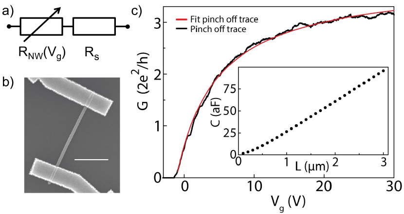
InSb nanowire FETs are fabricated on a heavily doped Si substrate (used as a global back-gate) terminated with a 285-nm-thick dry thermal SiO2 (Fig. 1b). The substrate is patterned with alignment markers prior to nanowire deposition. Nanowires are positioned on the substrate using a micro-manipulator [35]. Two terminal contacts are realized by electron beam lithography, metal evaporation (Ti/Au 5/145 nm) and lift-off. Argon plasma etching is employed prior to contact deposition. Further details about the fabrication process and the measurements can be found in Supplementary Text 1 and 2, respectively.
Due to the absence of a surface accumulation layer in InSb nanowires, an interface resistance of a few kilo ohms cannot be eliminated upon contacting the nanowire [36]. Such interface resistances are known to reduce the transconductance, resulting in an underestimation of the intrinsic mobility [37, 38]. Moreover, at a temperature of 4 K universal conductance fluctuations complicate the extraction of mobility from transconductance. We therefore tailor the extraction of field effect mobility to our InSb nanowire FETs [39]. We model the interface resistances by a resistor with a fixed value (no gate voltage dependence), connected in series to the nanowire channel. A substantial part of the device resistance at high gate voltage stems from the interface resistances, strongly affecting the gate voltage dependent conductance. This complicates accounting for a possible change of mobility with gate voltage. We therefore assume a mobility independent of gate voltage. The device conductance is then given by (see also Fig. 1a)
| (3) |
This equation allows for extraction of field effect mobility using a fit to the measured (). Here, the mobility , the interface resistances , and the threshold voltage are the free fit parameters. We restrict the fitting range to 100 k. We independently calculate the capacitance from a finite element model of the device (see Fig. 1c inset), where we take into account that quantum confinement in our nanowires reduces the classical capacitance by [40, 41]. Neglecting quantum effects in our capacitance calculation would lower the extracted mobility values by . Further details on the calculation of the capacitance can be found in Supplementary Text 3. We compared the mobility values extracted by a fit using eq. 3 with the mobility values obtained from peak transconductance, a common method to extract nanowire mobility, and found matching results (see Supplementary Text 4). For a representative fabrication run, mean forward mobility of 11 devices is found to be cm2/Vs using our fit method, whereas peak-transconductance method yields 2.7 (1.9) cm2/Vs with (without) taking into account the interface resistances. Our fit method, however, differs from peak transconductance method where the mobility is extracted from the maximum value of the transconductance using a small gate voltage range. Because we consider the transconductance in a wide gate voltage range by fitting a large section of (), the extracted mobility is insensitive to small conductance fluctuations. This is contrary to the peak transconductance where conductance fluctuations greatly affect the extracted mobility. We show in Supplementary Text 5 that our simple model with gate voltage-independent interface resistances is a valid approximation for our measurements. However, despite our thorough analysis a general drawback of field effect mobility remains: the uncertainty in the calculated capacitance value affects the extracted mobility directly. Nanowires suffer from this drawback as their small dimensions do not allow a straightforward experimental extraction of capacitance.
To determine what limits the mobility in our devices, we systematically studied the effect of various experimental parameters by measuring 10 devices simultaneously fabricated on the same substrate. We then change one parameter at a time for each fabrication run to deduce its effect on the field effect mobility.
3 Results and discussions
3.1 Nanowire surface and adsorption
Nanowire conductivity at room temperature is known to increase after evacuation of the sample space following mounting of devices [17, 42]. We find that evacuation also strongly affects () at low temperature (4 K). Comparing the () measured for short and long sample space evacuation time prior to cool down, we observe a steeper increase of conductance with gate voltage after long-time evacuation (Fig. 2a). Considering a number of devices on the same measurement chip, we find almost a doubling of the mobility values after long-time sample evacuation (Fig. 2b). The re-exposure of samples to air after long-time evacuation results in a reduction of mobility (Fig. 2c) with values very similar to those obtained from the initial measurements with a short-time sample space evacuation. The transconductance is larger when the gate is swept from low towards high voltages (forward sweep direction) leading to higher mobility compared to the case of sweeping from high gate voltages to low (reverse sweep direction) (Fig. 2c). Moreover, after long-time evacuation a shift of the threshold voltage towards more negative values is observed (Fig. 2d) together with a reduced hysteresis (Fig. 2e). Both the threshold voltage and the hysteresis regain their initial values obtained from short-time evacuation once the sample is re-exposed to air, similar to the extracted mobility: exposing the devices to air has a reversible effect on the field effect transport parameters we extract from the fits. All extracted fit parameters can be found in Supplementary Table 1.
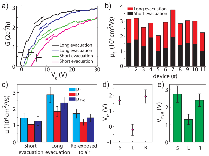
A hysteresis in transconductance dependent on ambient conditions has been studied before by Kim et al [43] and Wang et al [44], and was attributed to the adsorption of water onto the nanostructure and onto the SiO2 substrate. Evacuation of the sample environment leads to desorption of water, thereby reducing the hysteresis. However sample evacuation alone is insufficient to fully remove the adsorbed water. The similarities between our observations and those reported by Wang et al and Kim et al, considering both the influence of gate voltage sweep direction on the shift of the threshold voltage, as well as the reduction of hysteresis with evacuation time and the reversibility of the effect when reexposing samples to air, strongly suggest that the field effect transport is affected by molecules adsorbed to the nanowire and/or the SiO2 substrate. Water is highly likely to be the main adsorbate because reexposing the device to ambient atmosphere following long evacuation time of sample space yields values of mobility, threshold voltage and hysteresis similar to those obtained from the measurements with short evacuation time. InSb nanowires have however also shown decreased conductance in response to isopropanol and acetone [31].
It is an open question how adsorbates affect device conductance at low temperature. The alignment of polar molecules by gate electric field may result in an additional gating [44]. However, the mechanism through which such alignment causes hysteresis is not clear. Another scenario is charge trapping by adsorbed molecules [43]. Such trapping could possibly lead to an asymmetry between forward and reverse sweep direction, yielding the observed hysteresis and sweep direction dependent mobility. The observed trapping mechanism is likely to have a long response time, as our measurements are taken at relatively low gate voltage sweep rates (120 mV/s). Unlike refs. [32, 43, 44], we find no dependence on sweep rate for rates between 3 – 600 mV/s. Nonetheless, repeated measurements yield the same , implying that between scans the traps are emptied.
3.2 Substrate cleaning
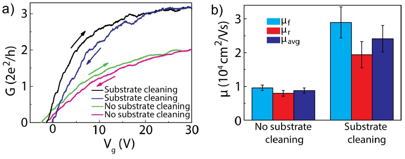
We further find that cleaning of Si/SiO2 substrates by remote oxygen plasma prior to nanowire deposition results in an enhanced gate dependence of low-temperature conductivity. Fig. 3a shows () curves of individual devices, while Fig. 3b shows an average over extracted mobilities obtained from measurements of 10 FETs with and without substrate cleaning. All other fabrication and measurement steps are the same for both sets of devices. The remote oxygen plasma most probably removes hydrocarbons that remain on the substrates after fabrication of alignment markers or during storage of samples in a polymer-containing environment. We verified that the oxygen plasma cleaning does not decrease the thickness of the SiO2 gate dielectric within the measurable range nm.
3.3 Contact spacing
A correlation between FET source-drain contact spacing and extracted field effect mobility is found (Fig. 4). Although the spread in mobility at a given contact spacing is substantial, an overall increase of extracted mobility is observed with increasing contact spacing. To determine whether the dependence of the field effect mobility on contact spacing originates from the length of the used nanowire, FETs with short (1 m) contact spacing were realized both on short wires, and on long wires using three contact electrodes resulting in two FETs in series. Devices made from both long and short wires with 1 m contact spacing give similar mobility (see Fig. 4). The contact spacing dependence is thus a device property rather than a nanowire property.
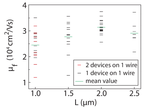
A reduced mobility for short contact spacing is expected when transport is (quasi-)ballistic rather than diffusive [45, 46]. We have observed ballistic transport in our wires [36] with a device geometry and measurement conditions different from those here. Here we expect quasi-ballistic transport in our devices with a mean free path comparable to nanowire diameter 0.1 m. While devices with are preferable, our InSb nanowires can currently not be grown longer than 3.5 m. However, while for channel length of 1 m (quasi-)ballistic effects may play a role, mobility values obtained from our devices with longer contact spacing yield a better estimate of field effect mobility. Moreover, effects related to the metal contacts are expected to play a larger role in devices with short contact spacing and can possibly contribute to the observed decrease of () in short channel devices. Possible explanations are that (1) the contacts reduce the capacitance of short devices more than expected from the Laplace simulations (in which the nanowire is assumed to be metallic) or (2) electrons are injected from and absorbed over a finite length underneath the contacts, leading to an effective larger than the contact spacing.
3.4 Reproducibility
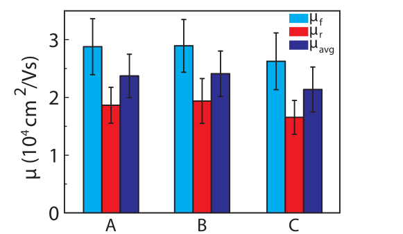
Altogether, cleaning the SiO2 substrate before wire deposition and applying a long sample evacuation time yields cm2/Vs for devices with a contact spacing m. This mobility is the average value of cm2/Vs (see Fig. 4) and cm2/Vs. These high mobilities result from measurements of 15 devices fabricated in different fabrication runs (see Supplementary Text 6 for details) using the same fabrication recipe. Fig. 5 demonstrates the reproducibility of our results: mobility obtained from three different fabrication runs are very similar. The optimized nanofabrication recipe as well as an overview of all the parameters extracted from the fits to the conductance vs. gate voltage curves that yield Fig. 5 are given in Supplementary Text 1 and Supplementary Table 2, respectively.
4 Conclusions and outlook
Low-temperature field effect mobility of InSb nanowires is extracted by measuring the conductance as a function of gate voltage. Taking surface adsorption and substrate cleaning into consideration, an optimized nanofabrication recipe has been obtained yielding average field effect mobilities of cm2/Vs. It is demonstrated that the obtained mobility values are highly reproducible.
As we show that surface adsorption has a large impact on field effect mobility, further studies should be directed towards minimizing the adsorbates and analysis of surface properties. An improved design of the measurement setup allowing for heating and better evacuation of the sample space is likely to facilitate a further desorption of adsorbates. Exposing the devices to UV-light during evacuation, which may assist desorption, can also be investigated [31]. Further, passivating the nanowire surface by removing the native oxide followed by application of a high quality dielectric likely reduces surface adsorption. Possible methods are atomic hydrogen cleaning [47] or chemical etching followed by dielectric deposition [48]. Alternatively, by suspending the nanowires above a metallic gate using vacuum as a dielectric, one can minimize the effects of the substrate adsorption, leaving the wire adsorption as the predominant constituent affecting the field effect mobility. In the case of adsorbates creating a fluctuating potential profile along the wire resulting in charge scattering, a core-shell structure is expected to yield a higher field effect mobility because the potential fluctuations due to adsorbates are spatially separated from the channel owing to the shell. Finally, to study the surface composition of the nanowire and the substrate, x-ray photoelectron spectroscopy or Auger electron spectroscopy could be used [49].
Acknowledgement
We thank K. Zuo, D. Szombati, V. Mourik, A. Geresdi and J. W. G. van den Berg for preliminary studies and fruitful discussions. This work has been supported by Dutch Organisation for Scientific Research (NWO), Foundation for Fundamental Research on Matter (FOM), European Union Seventh Framework Programme under grant agreement no. 265073 (NANOWIRING), and Microsoft Corporation Station Q.
References
References
- [1] L. Hofstetter, S. Csonka, J. Nygård and C. Schönenberger 2009 Cooper pair splitter realized in a two-quantum-dot Y-junction Nature 461 960-963
- [2] Y.-J. Doh, J. A. van Dam, A. L. Roest, E. P. A. M. Bakkers, L. P. Kouwenhoven and S. De Franceschi 2005 Tunable supercurrent through semiconductor nanowires Science 309 272-275
- [3] S. Nadj-Perge, S. M. Frolov, E. P. A. M. Bakkers and L. P. Kouwenhoven 2010 Spin-orbit qubit in a semiconductor nanowire Nature 468 1084-1087
- [4] R. M. Lutchyn, J. D. Sau and S. Das Sarma 2010 Majorana fermions and a topological phase transition in semiconductor-superconductor heterostructures Phys. Rev. Lett. 105 077001
- [5] Y. Oreg, G. Refael and F. von Oppen 2010 Helical liquids and Majorana bound states in quantum wires Phys. Rev. Lett. 105 177002
- [6] E. Majorana 1937 Teoria simmetrica dell’elettrone e del positrone. Nuovo Cimento 14 171-184
- [7] V. Mourik, K. Zuo, S. M. Frolov, S. R. Plissard, E. P. A. M. Bakkers and L. P. Kouwenhoven 2012 Signatures of Majorana fermions in hybrid superconductor-semiconductor nanowire devices Science 336 1003-1007
- [8] M. T. Deng, C. L. Yu, G. Y. Huang, M. Larsson, P. Caroff and H. Q. Xu 2012 Anomalous zero-bias conductance peak in a Nb-InSb nanowire-Nb hybrid device Nano Lett. 12 6414-6419
- [9] H. O. H. Churchill, V. Fatemi, K. Grove-Rasmussen, M. T. Deng, P. Caroff, H. Q. Xu and C. M. Marcus 2013 Superconductor-nanowire devices from tunneling to the multichannel regime: Zero-bias oscillations and magnetoconductance crossover Phys. Rev. B 87 241401(R)
- [10] J. D. Sau, S. Tewari and S. Das Sarma 2012 Experimental and materials considerations for the topological superconducting state in electron- and hole-doped semiconductors: Searching for non-Abelian Majorana modes in 1D nanowires and 2D heterostructures Phys. Rev. B 85 064512
- [11] A. C. Potter and P. A. Lee 2011 Engineering a p+ip superconductor: Comparison of topological insulator and Rashba spin-orbit-coupled materials Phys. Rev. B 83 184520
- [12] N. W. Ashcroft and N. D. Mermin 1976 Solid state physics New York: Holt, Rinehart and Winston
- [13] C. Blömers, T. Grap, M. I. Lepsa, J. Moers, S. Trellenkamp, D. Grützmacher, H. Lüth and T. Schäpers 2012 Hall effect measurements on InAs nanowires Appl. Phys. Lett. 101 152106
- [14] K. Storm, F. Halvardsson, M. Heurlin, D. Lindgren, A. Gustafsson, P. M. Wu, B. Monemar and L. Samuelson 2012 Spatially resolved Hall effect measurement in a single semiconductor nanowire Nature Nanotech. 7 718-722
- [15] S.M. Sze 1981 Physics of semiconductor devices 2nd ed. (New York: Wiley)
- [16] M. D. Schroer and J. R. Petta 2010 Correlating the nanostructure and electronic properties of InAs nanowires Nano Lett. 10 1618-1622
- [17] A. V. Kretinin, R. Popovitz-Biro, D. Mahalu and H. Shtrikman 2010 Multimode Fabry-Perot conductance oscillations in suspended stacking-faults-free InAs nanowires Nano Lett. 10 3439-3445
- [18] H. Shtrikman, R. Popovitz-Biro, A. V. Kretinin and P. Kacman 2011 GaAs and InAs Nanowires for ballistic transport IEEE J. Selected Top. Quant. Electron. 17 922-934
- [19] N. Gupta, Y. Song, G. W. Holloway, U. Sinha, C. M. Haapamaki, R. R. Lapierre and J. Baugh 2013 Temperature-dependent electron mobility in InAs nanowires Nanotechnology 24 225202
- [20] M. J. L. Sourribes, I. Isakov, M. Panfilova, H. Liu and P. A. Warburton 2014 Mobility enhancement by Sb-mediated minimisation of stacking fault density in InAs nanowires grown on silicon Nano Lett. 14 1643-1650
- [21] A. C. Ford, S. B. Kumar, R. Kapadia, J. Guo and A. Javey Observation of degenerate one-dimensional sub-bands in cylindrical InAs nanowires Nano Lett. 12 1340-1343
- [22] S. Chuang, Q. Gao, R. Kapadia, A. C. Ford, J. Guo and A. Javey 2013 Ballistic InAs nanowire transistors Nano Lett. 13 555-558.
- [23] M. Bar-Sadan, J. Barthel, H. Shtrikman and L. Houben 2012 Direct imaging of single Au atoms within GaAs nanowires Nano Lett. 12 2352-2356
- [24] F. Wang, S. Yip, N. Han, K. Fok, H. Lin, J. J. Hou, G. Dong, T. Hung, K. S. Chan and J. C. Ho 2013 Surface roughness induced electron mobility degradation in InAs nanowires Nanotechnology 24 375202
- [25] X. Jiang, Q. Xiong, S. Nam, F. Qian, Y. Li and C. M. Lieber InAs/InP radial nanowire heterostructures as high electron mobility devices Nano Lett. 7 3214-3218
- [26] J. W. W. van Tilburg, R. E. Algra, W. G. G. Immink, M. A. Verheijen, E. P. A. M. Bakkers and L. P. Kouwenhoven 2010 Surface passivated InAs/InP core/shell nanowires Semicond. Sci. Technol. 25 024011
- [27] Y. Li, J. Xiang, F. Qian, S. Gradecak, Y. Wu, H. Yan, D. A. Blom and C. M. Lieber 2006 Dopant-free GaN/AlN/AlGaN radial nanowire heterostructures as high electron mobility transistors Nano Lett. 6 1468-1473
- [28] G. W. Gobeli and F. G. Allen 1965 Photoelectric properties of cleaved GaAs, GaSb, InAs, and InSb surfaces; Comparison with Si and Ge Phys. Rev. 137 A150-A158
- [29] S. R. Plissard, D. R. Slapak, M. A. Verheijen, M. Hocevar, G. W. G. Immink, I. van Weperen, S. Nadj-Perge, S. M. Frolov, L. P. Kouwenhoven and E. P. A. M. Bakkers 2012 From InSb nanowires to nanocubes: looking for the sweet spot Nano Lett. 12 1794-1798
- [30] D. Car, J. Wang, M. A. Verheijen, E. P. A. M. Bakkers and S. R. Plissard 2014 Rationally designed single-crystalline nanowire networks Adv. Mater. 26 4875
- [31] M. V. Penchev 2012 Ph.D. thesis University of California, Riverside
- [32] S. A. Dayeh, P. K. L. Yu, E. T. Yu and D. Wang Transport properties of InAs nanowire field effect transistors: The effects of surface states Journ. Vac. Sci. Technol. B 25 1432
- [33] J. Du, D. Liang, H. Tang, X. P. A. Gao 2009 InAs nanowire transistors as gas sensor and the response mechanism Nano Lett. 9 4348-4351
- [34] P. Offermans, M. Crego-Calama, S. H. Brongersma 2010 Gas Detection with vertical InAs nanowire arrays Nano Lett. 10 2412-2415
- [35] K. Flöhr, M. Liebmann, K. Sladek, H. Y. Günel, R. Frielinghaus, F. Haas, C. Meyer, H. Hardtdegen, T. Schäpers, D. Grützmacher and M. Morgenstern 2011 Manipulating InAs nanowires with submicrometer precision Rev. Sci. Instrum. 82 113705
- [36] I. van Weperen, S. R. Plissard, E. P. A. M. Bakkers, S. M. Frolov and L. P. Kouwenhoven 2013 Quantized conductance in an InSb nanowire Nano Lett. 13 387-391
- [37] D. K. Schroder 2006 Semiconductor Material and Device Characterization 3rd ed. New York: John Wiley & Sons
- [38] W. Lu, P. Xie and C. M. Lieber 2008 Nanowire transistor performance limits and applications IEEE Trans. Electron Dev. 55 2859-2876
- [39] S. R. Plissard, I. van Weperen, D. Car, M. A. Verheijen, G. W. G. Immink, J. Kammhuber, L. J. Cornelissen, D. B. Szombati, A. Geresdi, S. M. Frolov, L. P. Kouwenhoven and E. P. A. M. Bakkers 2013 Formation and electronic properties of InSb nanocrosses Nature Nanotech. 8 859-864
- [40] L. Wang, D. Wang and P. M. Asbeck 2006 A numerical Schrödinger-Poisson solver for radially symmetric nanowire core-shell structures Solid-State Electron. 50 1732-1739
- [41] D. Eeltink 2013 M.Sc. thesis Delft University of Technology
- [42] S. Nadj-Perge 2010 Ph.D. thesis Delft University of Technology
- [43] W. Kim, A. Javey, O. Vermesh, Q. Wang, Y. Li and H. Dai 2003 Hysteresis Caused by Water Molecules in Carbon Nanotube Field-Effect Transistors Nano Lett. 3 193-198
- [44] D. Wang, Y.-L. Chang, Q. Wang, J. Cao, D. B. Farmer, R. G. Gordon and H. Dai 2004 Surface chemistry and electrical properties of germanium nanowires J. Am. Chem. Soc. 126 11602-11611
- [45] M. Shur 2002 Low ballistic mobility in submicron HEMTs IEEE Electron Device Lett. 23 511-513
- [46] Z. Chen and J. Appenzeller 2008 Mobility extraction and quantum capacitance impact in high performance graphene field-effect transistor devices IEEE IEDM Technical Digest 21.1 509-512
- [47] M. Hjort 2014 Ph.D. thesis Lund University
- [48] C. H. Hou, M. C. Chen, C. H. Chang, T. B. Wu, C. D. Chiang and J. J. Luo 2008 Effects of Surface Treatments on Interfacial Self-Cleaning in Atomic Layer Deposition of Al2O3 on InSb J. Electrochem. Soc. 155 G180-G183
- [49] S. Chu, G. Wang, W. Zhou, Y. Lin, L. Chernyak, J. Zhao, J. Kong, L. Li, J. Ren and J. Liu 2011 Electrically pumped waveguide lasing from ZnO nanowires Nature Nanotech. 6 506-510