Programming the Adapteva Epiphany 64-core Network-on-chip Coprocessor
Abstract
In the construction of exascale computing systems energy efficiency and power consumption are two of the major challenges. Low-power high performance embedded systems are of increasing interest as building blocks for large scale high-performance systems. However, extracting maximum performance out of such systems presents many challenges. Various aspects from the hardware architecture to the programming models used need to be explored. The Epiphany architecture integrates low-power RISC cores on a 2D mesh network and promises up to 70 GFLOPS/Watt of processing efficiency. However, with just 32 KB of memory per eCore for storing both data and code, and only low level inter-core communication support, programming the Epiphany system presents several challenges. In this paper we evaluate the performance of the Epiphany system for a variety of basic compute and communication operations. Guided by this data we explore strategies for implementing scientific applications on memory constrained low-powered devices such as the Epiphany. With future systems expected to house thousands of cores in a single chip, the merits of such architectures as a path to exascale is compared to other competing systems.
Index Terms:
Network-on-chip ; Epiphany ; Stencil ; Parallella ; Matrix-Matrix MultiplicationI Introduction
The Epiphany architecture comprises a low power, multi-core, scalable, parallel, distributed shared memory embedded system created by Adapteva[1]. The Epiphany IV 64-core Network-on-chip (NoC) coprocessor contains 64 cores (referred to as eCores) organized in a 2D mesh with future versions expected to house up to 4096 eCores. The Parallella System-on-module (SoM) board[1] combines the Epiphany IV chip with a host ARM processor housed in a Zynq System-on-chip. An earlier development prototype of the Parallella uses an FPGA mezzanine “daughter” card (FMC) housing the Epiphany IV, attached to a ZedBoard [2]. In this paper we report our evaluation of the hardware characteristics and software environment of the Epiphany system from the perspective of an application program developer using the ZedBoard and FMC daughter card setup.
To assess the performance of the Epiphany system we implement a stencil based scientific application kernel and a parallel matrix multiplication kernel. Stencil kernels apply regular operations on a grid, and are common to a wide range of high performance computing applications, and have similar characteristics to other applications such as image processing. They require good floating point performance but also fast communications. Parallelization is usually via domain decomposition with communications primarily between adjacent domains. Such applications might be expected to map well to the 2D mesh topology of the Epiphany coprocessor.
Multiplication of matrices is a fundamental operation which is used in many scientific applications. Here, we implement and extend the parallel matrix multiplication algorithm described by Sapir [3] which involves data communication between neighbouring cores following Cannon’s algorithm [4]. The relatively small memory per core presents some challenges in implementing this, necessitating careful usage of available memory buffer space for communication between cores.
In the following sections we give a brief overview of the Epiphany system and the programming model it supports. We then discuss how this impacts on program design. In Section V we outline micro-benchmarks used to assess the basic performance of the Epiphany coprocessor. Section VI details the parallel stencil implementation along with performance results. Section VII details the parallel matrix multiplication implementation along with performance results. Section VIII highlights related work and contrasts the Epiphany with similar many-core energy efficient systems. Conclusions and future work are outlined in Section IX.
II System Architecture
Both the Parallella and the prototype ZedBoard consist of a Zynq SoC, shared memory and the Epiphany NoC coprocessor as shown in Figure 1.

The Xilinx Zynq 7000 series SoC contains a dual-core ARM Cortex-A9 CPU running at 800 MHz on the Parallella and 667 MHz on the ZedBoard, with standard on-chip peripherals such as USB 2.0, Ethernet, UART, MIO, AXI BUS, GPIO, HDMI, JTAG etc. It also contains a Field Programmable Gate Array (FPGA) which is used to implement the “Glue-Logic” and eLink protocol required to interface with the Epiphany coprocessor. In addition, the FPGA implements the AXI master interface, AXI slave interface and a HDMI controller.
The Epiphany NoC has a 2D array of eCores connected to each other by a mesh network-on-chip. Each eCore consists of a RISC CPU, 32 KB of local scratchpad memory, a Direct Memory Access (DMA) engine, and a network interface to an eMesh router. No cache is present. Each eMesh router provides three network communication channels; an on-chip write network (in blue), an off-chip write network (in green) and a read request network (in red). The eCore CPU is super-scalar and can execute two floating-point operations and a 64-bit memory load/store operation in every clock cycle. Scratchpad memory can theoretically provide up to 32 Bytes per clock cycle of bandwidth.
The Parallella SoM has 1 GB of DDR3 RAM, while the ZedBoard has 512 MB. The DRAM is partitioned such that Linux running on the ARM Cortex-A9 CPU has its own private O/S memory and the rest is accessible by both the ARM and Epiphany. Shared memory access for the Epiphany is handled by an eLink interface via the AXI bus and memory controller on the Zynq SoC. The Epiphany has a flat and unprotected memory map. Each eCore can address its local SRAM, other eCores’ SRAMs and shared off-chip DRAM.
III Programming Model
The Epiphany chip can be programmed using C, and has an SDK [1] that provides some basic programming primitives to facilitate writing parallelized C code for this architecture. Some of the key features of the SDK are:
-
•
Workgroup model: To program the eCores, workgroups are created by specifying the number of rows and columns of nodes and the location of the starting node of the group. The SDK provides functions to determine the ID and location of neighbouring eCores.
-
•
Memory addressing: All eCores share the same address space and it is possible to read and write directly to the local memory of another eCore. The SDK provides functions to obtain the global address of a memory location in another eCore’s local memory facilitating data transfer between the nodes.
-
•
Communication between eCores: The SDK provides APIs to transfer blocks of data between nodes and to the shared memory. These can be achieved by using either the CPU or the DMA engine. Two DMA channels are available in each node supporting both non-blocking and blocking DMA transfers.
-
•
Barriers: The SDK provides functions for setting synchronization points and barriers in the program.
-
•
Hardware Mutex: Mutexes are available to ensure mutual exclusion while accessing shared resources. The workgroup defines a memory location on the chip as the mutex object. The SDK provides functions to enable the eCores to utilize the mutex object.
-
•
Event Timers: Each eCore has two event timers that can be configured to independently monitor key events within the node such as clock counter, watchdog timing etc. This can be used to count the number of clock cycles which have elapsed during execution of a block of code.
The steps required to execute a program are:
-
1.
Host program creates a workgroup by specifying the number of rows and columns required and the position of the start node in the group.
-
2.
Host resets all the nodes and loads the device-side executable image into each eCore.
-
3.
Host signals all the eCores in the workgroup to start execution
-
4.
Host communicates with each eCore either by accessing the core’s local memory or using the shared memory.
-
5.
Once the execution is complete, the host is signalled. The host reads the result either directly from each eCore’s local memory or from the shared memory.
IV Programming Considerations
The Epiphany eCore architecture presents some interesting challenges to implementing high performance numerical codes. The main limitation is the relatively small 32KBytes of local RAM per eCore which must be divided between program code, data and stack. Although each eCore has access to the entire 32-bit address space, performance drops off when accessing non-local memory. Within each eCore the supplied linker scripts allow the programmer to control which parts of the code and data are to reside in which specific bank of local memory and which parts are to be located in slower off-chip shared memory.
In its current form the Epiphany eCore does not include hardware support for integer multiply, floating point divide or any double-precision floating point operations. This design decision frees up silicon for other uses, e.g. for additional cores. Obviously the implication of this varies from application to application.
Maximum floating-point performance is achieved when each eCore is performing a stream of Fused-Multiply-Add (FMADD) instructions with simultaneous 64-bit load or store operations in each clock cycle. At 600MHz on a 64-core Epiphany this corresponds to a peak of 76.8 single-precision GFLOPS. The ability of the compiler to optimise code and achieve this is another matter.
IV-A Program Structure
The development environment requires (at least) two C programs to be written: one for the host CPU and one or more “kernels” for running on the eCore nodes.
An application code would typically perform all of its initialization and outer loops on the host CPU, with the inner-most, numerical-intensive, loops running as kernels on the Epiphany eCore nodes. Lesser-used library functions required by the kernel can be located in slower, but more abundant, shared-memory.
IV-B Overcoming Memory Limitations
As indicated previously, the local eCore memory is implemented as four banks of 8KBytes each. Maximum performance can be obtained only when code is fetched from one bank whilst load/store and DMA operations are occurring to other banks.
This further restricts code size to 8 or 16KBytes, or between 2k and 8k instructions (depending on mix of 16-bit and 32-bit instruction words). The programmer needs to carefully allocate the use of these four local memory banks in order to achieve the best performance.
For example, the programmer could allocate one bank of local memory for code, two for data (“data1” and “data2”) and one for the stack and local variables. With such an arrangement the code can process data to/from “data 1”, while using DMA to move data in/out of “data 2”. When the processing and DMA are complete, the code can then go on to process “data 2” while using DMA to move result data out and new input data into “data 1”.
Adding further pressure on limited memory, branching (eg. in loops) costs 3 cycles, so should be avoided where possible by “unrolling” inner loops. However unrolling loops comes at a cost to code size. With such small amounts of memory available for code, it is necessary to finely tune the degree to which loops are unrolled. Directives to the C compiler can be used to determine the degree of loop unrolling.
Instructions can, however be fetched from the local memory of other eCores. Thus a novel approach may be to locate smaller fragments of non-innermost-loop code in unused portions of banks of local memory of eCores within a row. This code could then be executed, when required, with contention only between the eCores in that row. This would result in less contention for eMesh bandwidth than if all the eCores were executing code out of external shared memory.
IV-C Hardware/Software Operation
Codes for array processing often make use of product terms in array indices, for example, to calculate row offsets. Without hardware support for integer multiplication it is desirable to iterate through array elements in a regular matter using incremented offsets. Similarly where possible floating-point divide operations should be removed from inner loops or minimized. In both cases these are optimisations that can usually be carried out by a compiler.
In terms of the current lack of support for double-precision floating point arithmetic, there is really no sensible work-around. However, there is increasing evidence to suggest that for many calculations careful use of single precision floating point is sufficient [5, 6]. Also in the case of the Parallella and other Epiphany platforms, the dual-core ARM Cortex-A9 CPUs on the Zynq chip provide high-performance double-precision Vector Floating Point Units (VFPU), so codes with high single-precision requirements and more modest double-precision requirements may fit the Zynq-Epiphany combination well.
V Performance Experiments
Experimental Platform: A ZedBoard [2] evaluation module containing a Xilinx Zynq 7000 SoC XC7Z020-CLG484-1 with a daughter card [1] housing the Epiphany-IV 64-core 28nm (E64G401) was used for all experiments. The dual-core ARM Cortex-A9 present on the Zynq SoC runs at 667 MHz and the Epiphany eCores run at 600 MHz each. The board has 512 MB of DDR3 RAM which has 480 MB allocated as ARM Linux O/S private memory and 32 MB allocated as shared memory between ARM Linux and Epiphany eCores.
Compilers and Tools: The Epiphany SDK version 5.13 was used to perform all experiments. The ARM Cortex-A9 runs the Linux kernel version 3.3.0 and the Linaro root file system version 12.11. ARM GCC 4.6.3 is used to compile the host code and E-GCC 4.8.2 (Epiphany GCC) is used to compile the device code. Several compiler options are enabled for E-GCC, including -funroll-loops -falign-loops=8 -falign-functions=8 -fmessage-length=0 -ffast -math -ftree-vectorize -std=c99 ffp-contract=fast -mlong-calls -mfp-mode=round-near est -MMD -MP -fgnu89-inline. These enable optimizations including and not limited to loop unrolling, inlining functions etc.
V-A Network Performance
The eMesh Network-On-Chip has a 2D mesh topology with only nearest-neighbour connections. To evaluate the cost of routing messages from one eCore to another a small micro-benchmark was written. In this benchmark one eCore in the mesh writes data as a sequence of 32-bit transfers into the memory of another eCore. Once the transfers are complete, the source eCore writes to a specific location in the receiving eCore. The receiving eCore monitors this location, observes the change, and begins to write the data into the memory of the next eCore in the row. This process is repeated for all the mesh nodes with the boundary nodes transferring the message to the next row. This is repeated a number of times while the total data transferred and total mean time are recorded. Two methods are used to transfer the data between the two eCores - DMA and point-to-point writes. Pseudo code for the benchmark with point-to-point write transfers is given in Listing 1.
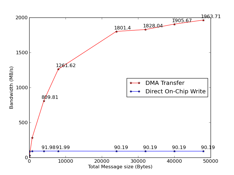
The bandwidths observed using the DMA and direct write methods as a function of message length for transfers between adjacent eCores are shown in Figure 2. For all but very small messages it is better to use DMA rather than issuing individual write instructions. For large messages DMA is able to achieve around 2GB/s transfer rates. Theoretically, with a 32-bit single word transfer per clock cycle, the DMA engine can provide a sustained data transfer rate of 2.4GB/sec at a clock speed of 600 MHz. With doubleword transfers it can provide a transfer rate of up to 4.8GB/sec.
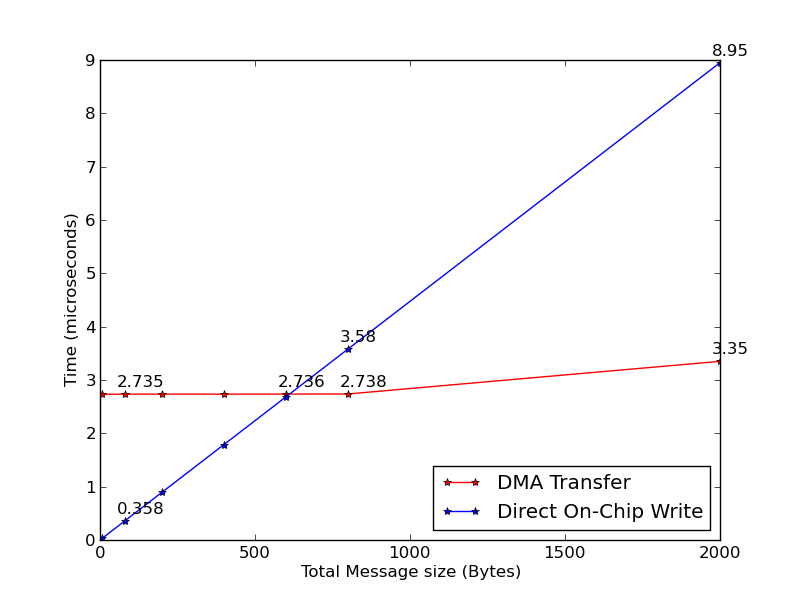
Latency is important for small data transfers. Figure 3 shows the latency for small message transfers. For transfers of less than about 500 bytes it is faster to write directly into the memory of an adjacent eCore rather than to use DMA transfers. Beyond 500 bytes, DMA is preferable.
In Table I we report the latency for an 80 byte message transferred from eCore 0,0 to one of the other cores in the grid. The Manhattan distance of each transfer is given. This shows surprisingly little effect of distance, although all transfers are relatively slow in terms of clock cycles.
| Node 1 | Node 2 | Manhattan Distance | Time per transfer (nsec) |
| 0,0 | 0,1 | 1 | 11.12 |
| 0,0 | 1,0 | 1 | 11.12 |
| 0,0 | 0,2 | 2 | 11.14 |
| 0,0 | 1,1 | 2 | 11.14 |
| 0,0 | 1,2 | 3 | 11.19 |
| 0,0 | 3,0 | 3 | 11.19 |
| 0,0 | 0,4 | 4 | 11.38 |
| 0,0 | 1,3 | 4 | 11.38 |
| 0,0 | 3,3 | 5 | 11.62 |
| 0,0 | 4,4 | 6 | 11.86 |
| 0,0 | 7,7 | 14 | 12.57 |
V-B External Shared Memory
As mentioned, the only way to get data in and out of the Epiphany chip is via the shared memory (unless external hardware is connected to the other eLink interfaces).
Much example code exists to showcase the performance of the memory system, but none to clearly show the performance when multiple eCores attempt to write to the external shared memory, over the single 8-bit wide, 600MHz (600MB/sec each direction) eLink, and how these accesses may be impacted by normal ARM CPU memory accesses to the shared DRAM.
Testing on the 64-core Epiphany-IV device housed on our system was hampered by the presence of Errata #0, as documented in the E64G401 Datasheet [1]: “Duplicate IO Transaction”. This is reported to affect all eCores in row 2 and column 2 (15 eCores total) in the 64-core device, for instruction fetches and data reads, but not for DMA operations, nor, apparently, for data writes.
Testing showed that location does matter when an eCore is attempting to write to the external shared memory. Nodes closer to column 7 and row 0 get the best write access to external DRAM. Nodes closer to column 7 always do better than eCores closer to row 0. With sufficient contention, many (all) eCores in rows 5 - 7 simply miss out on write slots.
In any case, the maximum write throughput to external shared memory achieved was 150MB/sec, exactly one quarter of the theoretical maximum of the 600MB/sec eLink.
To evaluate the relative share of the external memory interface that is allocated to each eCore for off-chip data transfers, a micro-benchmark was written. In this benchmark, four eCores (organized as ) continuously write blocks of 2KBytes as sequences of 4-byte stores to the external memory. This is done for a specific period of time (two seconds) and the utilization of the eLink by each mesh node is measured. The result is shown in Table II. The experiment is repeated with all 64 eCores writing simultaneously to the external memory and the results are shown in Table III. The effects of starvation are clearly evident.
| Mesh Node | Iterations | Utilization |
|---|---|---|
| 0,0 | 61037 | 0.41 |
| 0,1 | 48829 | 0.33 |
| 1,0 | 24414 | 0.17 |
| 1,1 | 12207 | 0.08 |
| Mesh Node (Total No) | Iterations | Utilization |
|---|---|---|
| 0,7 1,7 2,7 3,7 | 27460+ | 0.187 each |
| (8) | 3050+ | 0.021 each |
| (4) | 2040+ | 0.014 each |
| (8) | 100 - 1000 | |
| (9) | 10 - 100 | |
| (7) | 1 - 10 | |
| (24) | 0 |
VI Heat Stencil
We use the same stencil as in the Intel Teraflop paper [7]. In this benchmark a 5-point star (“+”) shaped stencil, with separate co-efficients per point, is applied to all data points in the grid. We reference the five points as Top, Left, Centre, Right and Bottom (T,L,C,R,B). Using and to reference points on a 2D Cartesian grid in the and directions and as the temperature, an update proceeds as follows:
The stencil kernel is mapped to the Epiphany architecture using a 2-dimensional domain decomposition. The grid of temperatures is stored in a 1-dimensional array in row-major order and is distributed equally among all the nodes. The host transfers the corresponding grid portion to the local memory of each eCore directly using the available API functions for data transfer. Once the grid is copied to the local memory, each eCore computes the values for the current iteration for all the grid points assigned to that eCore. This is followed by a communication phase.
Computation
Maximum floating point performance on the Epiphany architecture can only be achieved when using the FMADD instructions which effectively yields two Flops/cycle. This instruction multiplies two inputs from registers and accumulates the result into a third register, all in one instruction. It can be executed concurrently with certain other integer unit instructions, such as loads and stores, in a super-scalar manner.
Communication
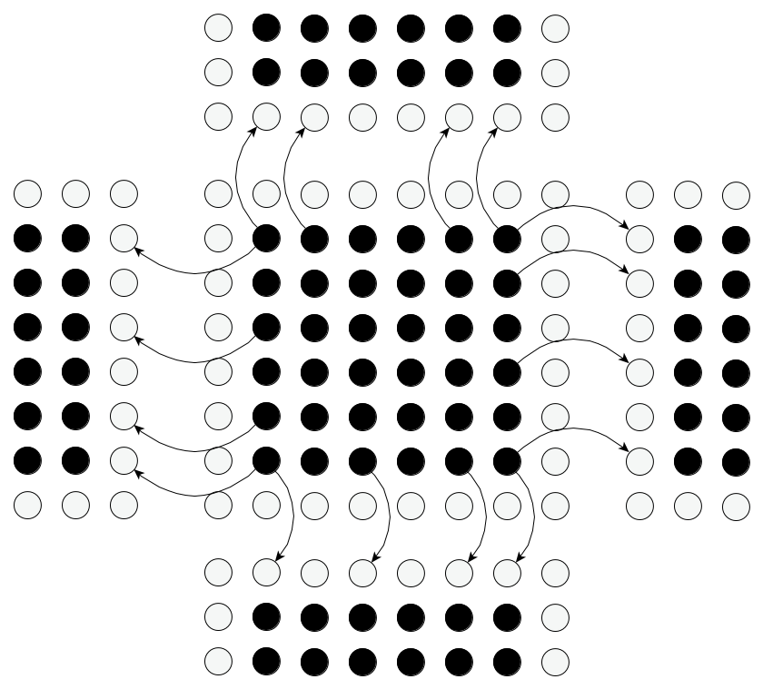
The computation is followed by a communication phase where the “edge” regions of the grid are transferred to the “boundary” regions of each of the four neighbouring eCores. Thus each eCore receives data from each of its neighbours as shown in Figure 4. An “in-place” algorithm is used where the result of the current iteration is stored back in the same array. Hence the transfers are started after the neighbours have completed their computation phase. In each iteration, a node is synchronized with each of its four neighbouring nodes. The transfers are achieved using the DMA engine, which transfers data to each neighbour in a chain. 64-bit double word transfers are used for the top and bottom boundary rows as they are stored in continuous memory locations, while 32-bit single word transfers are used for transferring the left and right boundary columns.
The following snippets of code illustrates how the communication and synchronization are performed.
The above steps are repeated for a number of iterations. After all the iterations are completed, the host reads the corresponding portion of the computed grid from each eCore and writes out the final result.
Discussion
Our first implementation was written in C, however the relatively immature compiler was only able to achieve a small fraction of peak. This code was replaced with a hand-tuned assembly code using the Epiphany instruction set. Grid sizes of were used where 20 was chosen based on the number of available registers and the latency of operations. Rows containing more than 20 elements are processed 20 at a time. The maximum number of rows, X, that can be processed on one eCore is driven by the number of elements per row and the available memory.
Experimentation showed that the register used for accumulating the result of the FMADD instruction cannot be used again as a Floating point unit (FPU) source or result register, or as the source of a store instruction for at least 5 cycles to avoid stalling the execution pipeline.
The eCore CPU has a total of 64 accessible 32-bit registers which can be used as single-precision floating point values, 32-bit signed or unsigned integers or as memory pointers, with various addressing modes. The Epiphany Architecture Reference manual recommends that some of these registers be used for parameter passing. Some registers are to be saved by the calling routine and some are to be saved by the called (“Callee”) routine. The only special register is r14, the Link Register, which contains the return address used in a “ReTurn” from Subroutine (RTS) instruction.
Experimentation with the e-gcc C compiler showed that the registers identified as requiring “Callee Saved” (22 of them) are only available if the special word “register” is prepended to local variable declarations. The four registers identified as “Reserved for constants” are not allocated and hence not used in any C code fragments we inspected.
Attaining Peak Performance
To attain peak FPU performance for the 5-point stencil, it is desirable to execute FMADD instructions for as long as possible. Branching costs 3 cycles, with a further cycle or two for decrementing a counter register. Therefore, inner loops should be unrolled as much as possible, modulo code memory size constraints.
We maximize the use of registers by buffering rows of input data into registers and accumulating the results in registers before writing out the final result. Our strategy is to buffer two rows of grid points whilst performing the five FMADD instructions per grid point. We use row lengths (stripes) of 20 points (a multiple of 5) and enforce a design goal that each grid data point is loaded into a register just once.
Five FMADD operations are performed on five consecutive T grid points, followed by five FMADDs on the respective L values, which is followed by the five C values, five R values and finally the five B values. After completing a run of five grid points, the accumulated results need to be saved and the accumulators cleared. This takes 10 cycles.
To avoid stalling the FPU, we immediately start a second run of five grid points, using a second set of five accumulators. This is effectively double-buffering the result accumulators, using 10 registers in total (r8 - r12 for the first set, r15 - r19 for the other).
During the execution of these 5 x 5 FMADD instructions, we use the “spare” integer operation slots to replace the five Top (T) grid points with the five Bottom (B) grid points, whilst leaving the seven middle (five each of Left, Centre, Right, with overlap) buffered values alone. We also use these spare slots to save the accumulated results from the previous five grid points and to clear the next five accumulators.
Use of row stripes
As mentioned earlier, we use row stripes of 20 points. Two rows of 20 data points, plus the “boundary” values at each end, requires a total of 44 registers to buffer the input data.
Before starting, registers r20 - r41 are pre-loaded with grid data for the top boundary row (T), and registers r42 - r63 with grid data for the middle row (L,C,R). As the FMADDs are performed on the five lots of T data buffered in the registers, and during the FMADDs of the L, C and R grid points, the T data in r20 - r41 is progressively replaced with the equivalent B data from the next row of grid data. These loads need to be complete before the five final FMADDs on the B data are performed.
At the commencement of the next row, r20 - r41 now contain the middle data (L, C, R) and r42 - r63 contain the new T data. During the processing of the FMADDs for this row, r42 - r63 are progressively replaced with B data from the next row. At the completion of the second row, the above registers will be in the same order as at the start, that is T data in r20 - r41 and L, C, R data in r42 - r63.
This constitutes one “unrolled” loop of 40 x 5 = 200 FMADD instructions and ideally the same number of cycles. The code for the loop is approximately 1300 bytes: 800 bytes for the 200 x 32-bit FMADD instructions, plus 480 bytes for 120 x 32-bit integer instructions performing loads, stores and clears, plus sundry others. There is also a 4 or 5 cycle loop “penalty” as a register is decremented and a conditional branch is made to the top of the loop.
Assembly code structure
Many attempts were made to implement the above operations in C. However, a number of issues were encountered.
The main issue was that the C compiler was reluctant to allow all 64 registers (63 not including the Stack Pointer) to be used. Hence there were a number of data move instructions in the resulting assembly code to block the dual-issuing of FPU and integer/data movement instructions.
The main problem with writing the code in assembly language was allocation of the registers. Minor code changes could result in large rewrites of register usage, which inevitably makes the code prone to errors.
To avoid writing too much code, two macros were written to perform each of the 5 x 5 FMADD runs. Calling them alternately, whilst keeping the sequencing of register numbers correct greatly simplified the code.
Each macro results in 25 FMADD instructions with 15 data movement instructions interleaved, for a total of 40 x 32-bit instructions, executing in 25 clock cycles and performing 50 Flops.
Stringing 4 pairs of these macros together results in 200 FMADDs, almost 1300 bytes of code and 400 Flops for two stripes of grid data.
The decrement and branching at the end of a run of two rows of the stripe adds 4 or 5 clock cycles and so a 2 or 2.5% overhead over 200 clocks.
Other Strategies
A variation on the design is to allow multiple (3) loads of each grid data point and to only buffer one row of the ”stripe”. This would allow the stripe to become up to 32 grid points wide, or more. 64-bit loads and stores can be used to make this possible, but more careful attention to data alignment in memory and register allocation would be required.
The initial implementation performs the stencil operation “in place”, overwriting the previous grid data with new data on each iteration.
By allowing full dual-buffering of the grid data, an assembly language stencil code with no per-row buffering can be implemented, allowing arbitrary width only limited by code memory size and per-core data memory size. The downside is that this approach requires twice as much memory per grid point, or the grid array is limited to half the size.
Further Observations
The assembly code 5-point star stencil can be trivially modified to perform any 5-point stencil within a area containing a grid point, such as a “X” shaped stencil, or an arrow.
To change the number of points in the stencil will require some re-writing. Decreasing the number of points will be relatively straight-forward. However, increasing the stencil to, say, a full 9-point stencil will possibly require some more registers, only currently possible by shortening the stripe width. It may be possible to load the various stencil co-efficients into registers from memory, as required, to increase the number of “points” per stencil.
Further Optimizations
At the completion of each iteration, the boundary row/columns of adjoining mesh nodes need to be updated with “edge” data from the new grid, whilst “edge” data from surrounding nodes needs to be copied to the boundary row/columns of the local grid. To do this more efficiently for the “in-place” algorithm, the boundary rows and columns can be double-buffered. This would allow the transferring of boundary data to neighbouring mesh nodes to commence, whilst those nodes may still be processing the current boundary data. Performance gains are likely to be modest, roughly the same as the difference between the results with and without communication discussed below.
VI-A Stencil Results
VI-A1 Floating Point Performance
Here, we compare the floating point performance of the stencil kernel for different configurations of grid sizes. The stencil is evaluated for 50 iterations. Using a row width of 20, as explained in Section VI, we run multiple stripes of , where X is the number of rows, one after the other to test larger grid sizes. Three scenarios are considered i) the performance on a single eCore as a function of grid size ii) the performance using all 64 eCores when running the same problem on each eCore, iii) the performance when running one grid across all 64 eCores including communication of the boundary region between eCores.
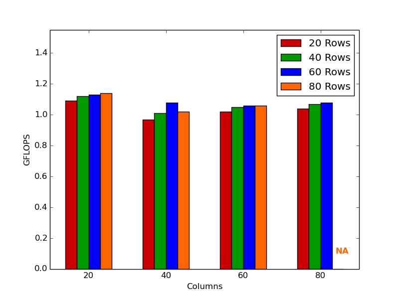
On a single eCore the performance ranges from 0.97-1.14 GFLOPS or between 81-95% of peak as shown in Figure 5. For small sizes, grids with more rows than columns tend to perform slightly better than the same size grid with more columns than rows. This is due to the overhead involved in performing multiple stripes of computation when column size is greater than 20 elements.
The performance of the code on all 64-eCores is shown in Figure 6. The darker colours show the performance of the stencil kernel including communication of boundary region. The lighter colours at the top of each bar shows the performance without communication of data.
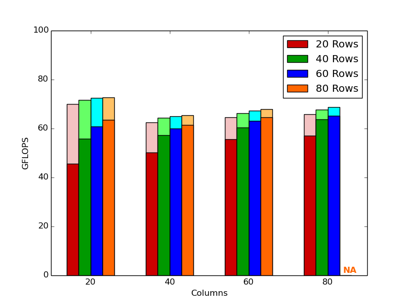
As expected, when the computations are replicated across all 64 cores with no communications performance scales linearly with a peak performance of 72.83 GFLOPS for a stencil containing 80 rows and 20 columns as shown in Figure 6. When boundary data is transferred during each iteration, this performance drops to 63.6 GFLOPS or 82.8% of peak. Thus the penalty associated with not overlapping communication and computation is roughly 9 GFLOPS. Due to the nature of 2D DMA block transfers, grids with more columns than rows show less performance drop than equivalent grids with more rows than columns.
VI-A2 Weak Scaling
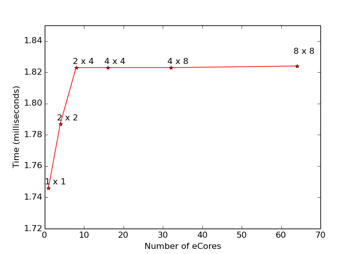
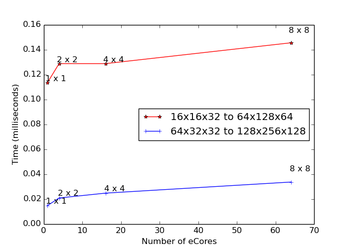
In this experiment, we increase the number of eCores from 1 to 64. The problem size is also increased accordingly from (1 eCore) to (64 eCores). The running time for each configuration is plotted in Figure 7 along with the configuration of the eCores (as ). Initially as the number of eCores increases from 1, the time taken increases due to the need for data communication between the eCores. This increase quickly levels out after 8 eCores () as communication between independent pairs of eCores can then be overlapped.
VI-A3 Strong Scaling
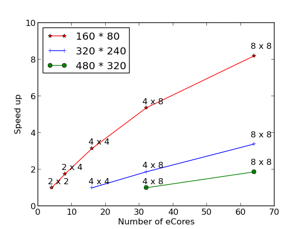
In this experiment, we increase the number of eCores from 1 to 64 while keeping the problem size fixed. This is repeated for three problem sizes. The speed-up achieved is shown in Figure 8 along with the configuration of the eCores. In all cases when the number of eCores is first doubled, a speed up of close to 2 is achieved with slightly better results achieved for the larger problem sizes. Further doubling of the number of eCores (when possible) achieves slightly less performance gain.
VII Matrix Multiplication
There are several parallel algorithms for matrix multiplication (matmul) on many-core systems. The approach used here is based on Sapir [3]. Our implementation operates at three levels:
-
•
At the most basic level, matrix blocks that fit inside a single eCore’s SRAM are multiplied. The requirement here is for a matrix multiply routine that is optimized for a single eCore both in terms of performance and memory usage.
-
•
At the next level, if the matrices are too large to be stored on a single eCore they are block distributed across the memory of multiple eCores. The algorithm proceeds by executing the kernel matrix multiply on each eCore for a given set of component blocks and then shuffling the blocks between eCores, repeating this process until the overall matrix multiplication is complete.
-
•
At the top level, if the matrices are too large to be stored on the entire chip a procedure analogous to the block wise algorithm outlined in the previous step is used to orchestrate movement of portions of the different matrices between off-chip shared memory and distributed eCore memory.
Below we expand on each of the three levels. For the purpose of what follows we consider matrices and with dimensions () and () respectively that are multiplied together to form with dimensions ().
Tuned single-core matmul kernel
As with the stencil code initial attempts were made to develop the eCore matrix multiply kernel in C. This however gave only 60 % of peak performance. Therefore the inner most loop of the matrix multiply was replaced with hand-tuned assembly code.
The assembly code loads 4 elements of the first matrix (matrix A) into 4 registers (r11,r12,r14 and r15) at a time. In turn each of these elements is multiplied with each element in the corresponding row of the second matrix (matrix B) with the intermediate results accumulated into 32 registers (r32-r63). In this process the rows of matrix B are loaded 8 elements at a time into registers r16-r23. Double-word loads are used allowing these 8 elements to be loaded in 4 clock cycles.
By pre-loading a few elements of matrix A and B, after each has been used the next unprocessed element is loaded into the freed registers. This enables load instructions and FMADD instructions to be interleaved, although care must be taken to ensure there are at least 5 cycles between using the same register for a load and a floating point instruction in order to avoid stalling the execution pipeline.
Each row of matrix A is loaded only once. Each element in the row is multiplied with all the elements in the corresponding row of matrix B. For example, the first element in a row of matrix A is multiplied with all the elements in the first row of matrix B and the intermediate results are accumulated in the first row of matrix C. The second element in a row of matrix A is multiplied with all the elements in the second row of matrix B, with the intermediate results being accumulated in the second row of matrix C. This means that for each row of matrix A, all the rows of matrix B need to be loaded from memory. Once all the elements in a row of matrix A are processed, the corresponding row of matrix C will have its final result. These values are now written out from the intermediate registers to memory using double-word store instructions and the registers are cleared for the next row of results.
Assembly code structure
As with the stencil, a macro was written to simplify the code. The macro is used to multiply an element of matrix A with all the elements in a row of matrix B. This involves 32 FMADD instructions and around 18 data movement instructions interleaved, resulting in 50 instructions executing 64 Flops in 32 cycles. For a matmul, the macro is expanded 32 times for computing each row of product matrix C, resulting in around 6.5 KBytes of assembly code and 2048 Flops for each row of result. At the end of a row, the code loops around to compute another row of the result incurring some overhead for the branch operation.
The disadvantage of writing in assembly is that the code is not very flexible to changes to the sizes of the operand matrices, the ’M’ dimension of matrix A being the only parameter which is configurable in the current code (as it is the loop count). To operate on different sizes of operand matrices, a few changes would need to be done to the assembly code including the macros in order to perform matrix multiplication efficiently for those sizes.
Memory Considerations
The operand matrices A and B, and the product matrix C are stored in the local memory of each eCore. Each eCore stores matrices of sizes up to using a total of 12 KBytes for storing the three matrices. The matrices are placed in different data banks. The operand matrices A and B are stored in data bank 2 and the product matrix C is stored in the last data bank (bank 3). The entire code takes around 11 KBytes of storage and occupies the first data bank (bank 0) and portions of the second data bank (bank 1) with the stack being allocated in the bottom half of bank 1. The size of the code has to be kept in mind while allocating memory for the operand matrices. This is especially important for the multi-core matmul version as described below.
On-chip multi-core matmul kernel
Using the single-core version as a building block, we implement a multi-core version in order to operate on bigger matrices. With each eCore able to store operands of sizes , we can work on matrices of size with all the data residing in the local memory of the 64 eCores.
Using capitals to refer to blocks of each matrix, expanding the matrix multiplication we obtain:
| (1) |
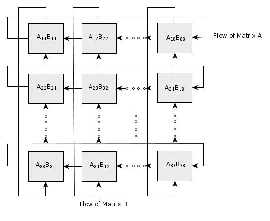
If each eCore is assigned a specific block of , we can see from equation 1 the blocks that are required by each eCore in order to complete the matrix product. In the implementation used here for each matrix a row of blocks is mapped to a row of eCores. The multiplication proceeds using Cannon’s algorithm, where blocks of A are progressively rotated around rows of eCores while blocks of B are rotated around columns of eCores. This process is illustrated in Figure 9.
For block sizes less than , double buffering is used for each of the operand matrices A and B in order to overlap computation and communication, thereby improving performance. Once an eCore completes its block computation, it transfers its portion of the matrix A and B to the second buffers of the neighbouring eCores without waiting for their computation to finish.
For blocks of size this is not possible. With each matrix requiring 4 KBytes of storage, storing the double-buffers for the operand matrices and the product matrix C would require a total of 20 KBytes of storage. However, since the size of the entire code including assembly is just over 13 KBytes, this doesn’t leave enough space for the double buffers and the stack. Hence an alternate buffering scheme was implemented.
In this scheme the matrix A is initially allocated in each eCore from 0x4000 to 0x4FFF and the matrix B from 0x5800 to 0x67FF (4 KBytes each) and the matrix C is allocated from 0x7000 to 0x7FFF. A buffer of 2 KBytes is allocated adjacent to each of these matrices, from 0x5000 to 0x57FF for matrix A and 0x6800 to 0x6FFF for matrix B. Once an eCore is ready to transmit its data, it starts transferring the lower 2 KBytes of the matrix A onto the buffer for matrix A of the neighbouring eCore on the left side. This is followed by a transfer of the lower 2 KBytes of matrix B to the buffer for matrix B of the neighbouring eCore above it as shown in Figures 10 and 11.
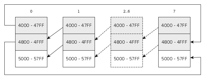
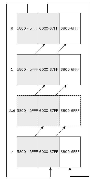
Once all the eCores complete these transfers, they start transferring the upper halves of the matrices A and B, replacing the lower halves of the corresponding matrices of the neighbours. The pointers to these two matrices are also changed accordingly. In the following iteration, communication is performed in the reverse order as illustrated in Figures 12 and 13. After changing the pointers to the two matrices again, the allocation of the matrices would be identical to the initial one.
Off-chip matmul kernel
For square matrices larger than there is insufficient memory to perform on-chip matrix multiplication, and it becomes necessary to page blocks of the matrices from off-chip shared memory. Here we exploit an analogous algorithm to that used to move blocks of matrices and between eCores for the on-chip case. Namely blocks of the product matrix are computed in turn by paging in blocks of and from shared memory. Thus in the case to complete one block of requires two blocks of both and to be read from shared memory.
VII-A Matrix Multiplication Results
VII-A1 Floating Point Performance
Here, we compare the floating point performance of the matrix multiplication kernel as a function of sizes of the operand matrices.
Single-core Floating Point Performance
The results for a single eCore are shown in Table IV. The maximum size of matrices that are multiplied is as mentioned earlier. On a single eCore the performance ranges from 0.85-1.15 GFLOPS or between 70-96% of peak.
| Matrix Dimensions | GFLOPS | Percentage of Peak (%) |
|---|---|---|
| 8 8 | 0.85 | 70.5 |
| 16 16 | 1.07 | 89.5 |
| 20 20 | 1.11 | 92.5 |
| 24 24 | 1.12 | 93.4 |
| 32 32 | 1.15 | 95.9 |
On-chip multi-core Floating Point Performance
Table V shows the floating point performance of the on-chip multi-core version which was implemented as detailed in Section VII. For grid sizes which are able to be fit on the local memory of the chip (up to ), the performance is around 85% including the data communication between pairs of eCores. (This does not include the time taken to transfer the initial operand matrices from the external shared memory to the chip). The table shows the per-core dimensions of the product matrix C and the number of eCores used to perform the multiplication. With a per-core matrix size of , the overall matrix dimensions would be when running on eCores, on eCores and on eCores.
| Matrix C | Num of eCores | |||||
|---|---|---|---|---|---|---|
| 2 2 | 4 4 | 8 8 | ||||
| (per-core) | GFLOPS | % | GFLOPS | % | GFLOPS | % |
| 8 8 | 1.25 | 26.1% | 5.07 | 26.4% | 20.30 | 26.4% |
| 16 16 | 3.12 | 65.1% | 12.76 | 66.5% | 51.41 | 66.9% |
| 20 20 | 3.58 | 74.7% | 14.36 | 74.8% | 57.62 | 75.0% |
| 24 24 | 3.84 | 80.1% | 15.43 | 80.4% | 62.17 | 81.0% |
| 32 32 | 4.06 | 84.7% | 16.27 | 84.7% | 65.32 | 85.1% |
The on-chip matrix multiplication of two matrices can be broken down into the computation of a matrix product by each eCore and the transfer of the two operand matrices A and B totalling 8 KBytes to the neighbouring eCore in each iteration. Considering 1.15 GFLOPS for the matrix product by a single eCore (from Table IV) and 2GB/s transfer rate between eCores (from results in Section V), the maximum theoretical performance can be estimated to be roughly 68 GFLOPS. From Table V, the performance achieved by the code is around 65 GFLOPS which is very close to the estimate.
Off-chip multi-core Floating Point Performance
The performance drops for sizes larger than due to the need for multiple transfers of blocks to and from the shared memory as the algorithm progresses as discussed earlier. The results are shown in Table VI. A per-core matrix size of is used to perform the multiplication of large matrices of sizes and . To build the result for the large matrix size , a per-core size of is used and hence the overall performance in GFLOPS is a bit worse than the other two cases. In all the cases, the off-chip memory transfer dominates the overall performance with around 86-90% of the total time taken being spent on the block DMA transfers in and out of shared memory and 10-13% of the total time taken being spent on the computation.
| Matrix C | GFLOPS | % of Peak | % Computation | % Shared Mem Transfers |
|---|---|---|---|---|
| 512 512 | 8.32 | 10.8 % | 12.8 % | 87.2 % |
| 1024 1024 | 8.52 | 11.1 % | 13.1 % | 86.9 % |
| 1536 1536 | 6.34 | 8.2 % | 10.9 % | 89.1 % |
To analyse the performance of the off-chip matrix multiplication, we consider the multiplication of two matrices. Each matrix can be considered as consisting of four blocks of elements. Each iteration in the outer-most loop in the algorithm involves transferring one block of matrix A and one block of matrix B from the shared memory to the chip and having all the 64 eCores perform parallel multiplication to produce an intermediate block result. The transfer of two blocks of elements (512 KBytes) takes around 0.0034 seconds at 150MBytes (from results in Section V). The computation of the block matrix product takes around 0.00051 seconds at 65.32 GFLOPS (from Table V). Thus the ratio of computation to off-chip transfers is roughly 1:6.5. From the result in Table VI the ratio of computation to off-chip data transfer is 1:6.8 which is very close to the estimate.
VII-A2 Weak Scaling
In this experiment, the number of eCores is increased from 1 to 64 while increasing the problem sizes accordingly. Two separate configurations are tested and the running time for each configuration is plotted in Figure 14. The problem sizes are shown as . Each of these problems are run (wherever possible) on an eCore configuration of , , and . In the first configuration, the problem size is increased from (1 eCore) to ( eCores). In the second configuration, the problem size is increased from (1 eCore) to ( eCores). The time taken increases initially due to increasing data communication between the eCores. This increase quickly levels out as communication between independent pairs of eCores is overlapped.
VII-A3 Strong Scaling
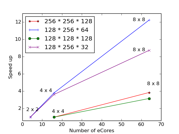
In this experiment, the number of eCores is increased from 1 to 64 while keeping the problem size fixed. This is repeated for four different problem sizes. Each of these problems are run (wherever possible) on an eCore configuration of , and . The speed-up achieved is shown in Figure 15. The problem sizes are shown as . When the number of eCores is quadrupled, a speed up of close to 4 is achieved. Better results are achieved for larger problem sizes as expected.
VIII Related Work and Comparison with other systems
Similar many-core coprocessor systems include the Intel 80-core terascale coprocessor [7], the 48-core single-chip cloud computer (SCC) [8, 9], the 64-core Tilera Tile64 SoC [10, 11], the recent Intel Xeon Phi accelerator [12]. Use of low power ARM based SoC processors [13] and many-core accelerators such as the TI C66X DSP [14, 15] for high performance computing are also of increasing interest. A comparison of some of these systems is shown in Table VII.
| TI C6678 Multicore DSP | Tilera 64-core chip | Intel 80-core Terascale Processor | Epiphany 64-core coprocessor | |
| Chip Power(W) | 10 | 35 | 97 | 2 |
| Cores | 8 | 64 | 80 | 64 |
| Max GFLOPS | 160 | 192 | 1366.4 | 76.8 |
| Clock Speed(GHz) | 1.5 | 0.9 | 4.27 | 0.6 |
The closest related work is that of Mattson et al. [7]. This paper describes the challenges in programming the Intel 80-core network-on-a-chip Terascale Processor. With 80 cores running at 4.27 GHz, Mattson et al. ran the same five-point star-shaped heat diffusion stencil kernel at 1 single precision TFLOPS while consuming 97 Watts. This is a significant contribution as it demonstrated that high performance could be delivered using such many-core coprocessors. It equates to a performance of just over 10 GFLOPS/watt. By contrast and assuming 2 watts power usage, the Epiphany system used here achieves roughly 32 GFLOPS/watt. (The actual power consumed by the chip has not been measured yet, although we are currently making efforts to profile the actual power consumption.)
In more general work on stencil implementations, Wittman et al. [16] explore the explicit use of shared caches in multicore systems for implementing a pipelined temporal blocking approach for stencil computation. This technique performs multiple in-cache updates on each grid point before the result is moved back to memory. Datta et al. [17] also look at improving stencil computation by examining tiling techniques that leverage both spatial and temporal blocking of computation in order to increase data reuse. Melot et al. [18] address the performance limitation seen on many-core processors due to the use of off-chip memory by implementing pipelined streaming computations. This work describes the advantages of employing an on-chip pipelined merge sort algorithm on the 48 core Intel SCC in an attempt to overcome the limitation of slow off-chip memory access.
We extended the work of Sapir[3], who describes a parallel matrix multiplication algorithm for matrices which are too large to be fit on the device memory. This involves block transfers between rows or columns of nodes using Cannon’s algorithm. The transfers are typically between nearest neighbours and is well suited for 2D mesh architectures such as the Epiphany. Algorithms such as SUMMA[19] and PUMMA[20] are well known distributed algorithms for matrix multiplication involving block distribution of the matrices between processors not necessarily arranged in a grid. SUMMA also has the advantage of requiring less workspace per node enabling larger problems to be run.
IX Conclusion & Future Work
In this paper, we explored the Adapteva Epiphany 64-core Network-on-chip coprocessor. Different strategies for stencil based application codes running purely on device memory were implemented. A tuned matrix multiplication kernel was implemented for multiplying matrices which fit in the device memory along with a buffering method to overcome the relatively small memory per core. Using this a building block, an algorithm for multiplying large matrices was implemented. Micro-benchmarks were used to evaluate the performance of several basic compute and communication operations on the Epiphany system. The process of mapping an application kernel to the Epiphany architecture was demonstrated. It was noted that the low-level C programming primitives available in the Epiphany SDK provided ease of use in programming the Epiphany. However, further work towards implementation of familiar programming models such as OpenCL [21] and the recently launched OpenMP Accelerator model [22] for the Epiphany is of great interest. Increasing problem sizes for stencil kernels and implementation of an efficient pipelined kernel for large problem sizes is also of interest. We aim to extend our current work by employing a pipelined algorithm for stencil computation using both spatial and temporal blocking in order to process much higher grid sizes. Such an algorithm would ensure that computation is performed for a number of iterations before the data is moved out of the local memory and new data is brought in. Multiple iterations of computation can be performed for those points for which dependent points are in the same block. When no more iterations are possible, another block would be streamed into the local memory to ensure that computation can move forward.
In our experiments, on-chip DMA bandwidth of 2 GBytes/s, off-chip shared memory access bandwidth of 150 MBytes/s and on-chip memory latency of 11 ns for nearest neighbour were observed. Floating point performance of roughly 64 GFLOPS (82% of peak) was achieved for an optimized stencil kernel involving communication of data and a performance of roughly 65 GFLOPS (85% of peak) was achieved for an optimized on-chip parallel matrix multiplication. This corresponds to a power efficiency of roughly 32 GFLOPS/Watt on the 64-core chip. However, extracting maximum performance out of the system requires considerable effort on the part of the programmer at this stage. The relatively slow external shared memory interface becomes a bottleneck when scaling to large problem sizes. If these are addressed, with future versions expected to scale to 4096 cores with a peak floating point performance of 5 TFLOPS and power efficiency of 70 GFLOPS/Watt, the Epiphany would be a promising platform for energy efficient high performance computing.
Acknowledgment
This work is supported in part by the Australian Research Council Discovery Project DP0987773.
References
- [1] Adapteva, “Epiphany Technical Reference Documents,” http://www.adapteva.com/all-documents.
- [2] ZedBoard, “ZedBoard Development Kit,” http://www.zedboard.org/product/zedboard.
- [3] Yaniv Sapir, “Scalable Parallel Multiplication of Big Matrices,” http://www.adapteva.com/white-papers/scalable-parallel-multiplication-of-big-matrices/.
- [4] L. E. Cannon, “A cellular computer to implement the kalman filter algorithm.” DTIC Document, Tech. Rep., 1969.
- [5] J. Dongarra, “The impact of multicore on math software and exploiting single precision computing to obtain double precision results,” in Parallel and Distributed Processing and Applications, ser. Lecture Notes in Computer Science, M. Guo, L. Yang, B. Di Martino, H. Zima, J. Dongarra, and F. Tang, Eds. Springer Berlin Heidelberg, 2006, vol. 4330, pp. 2–2. [Online]. Available: http://dx.doi.org/10.1007/11946441_2
- [6] A. BUTTARI, J. DONGARRA, J. K. J. LANGOU, J. L. P. LUSZCZEK, and S. TOMOV, “Exploiting mixed precision floating point hardware in scientific computations.”
- [7] T. G. Mattson, R. Van der Wijngaart, and M. Frumkin, “Programming the intel 80-core network-on-a-chip terascale processor,” in Proceedings of the 2008 ACM/IEEE conference on Supercomputing. IEEE Press, 2008, p. 38.
- [8] T. G. Mattson, M. Riepen, T. Lehnig, P. Brett, W. Haas, P. Kennedy, J. Howard, S. Vangal, N. Borkar, G. Ruhl et al., “The 48-core scc processor: the programmer’s view,” in Proceedings of the 2010 ACM/IEEE International Conference for High Performance Computing, Networking, Storage and Analysis. IEEE Computer Society, 2010, pp. 1–11.
- [9] S. R. Vangal, J. Howard, G. Ruhl, S. Dighe, H. Wilson, J. Tschanz, D. Finan, A. Singh, T. Jacob, S. Jain et al., “An 80-tile sub-100-w teraflops processor in 65-nm cmos,” Solid-State Circuits, IEEE Journal of, vol. 43, no. 1, pp. 29–41, 2008.
- [10] S. Bell, B. Edwards, J. Amann, R. Conlin, K. Joyce, V. Leung, J. MacKay, M. Reif, L. Bao, J. Brown et al., “Tile64-processor: A 64-core soc with mesh interconnect,” in Solid-State Circuits Conference, 2008. ISSCC 2008. Digest of Technical Papers. IEEE International. IEEE, 2008, pp. 88–598.
- [11] O. Serres, A. Anbar, S. Merchant, and T. El-Ghazawi, “Experiences with upc on tile-64 processor,” in Aerospace Conference, 2011 IEEE. IEEE, 2011, pp. 1–9.
- [12] A. Heinecke, K. Vaidyanathan, M. Smelyanskiy, A. Kobotov, R. Dubtsov, G. Henry, A. G. Shet, G. Chrysos, and P. Dubey, “Design and implementation of the linpack benchmark for single and multi-node systems based on intel® xeon phi coprocessor,” in Parallel & Distributed Processing (IPDPS), 2013 IEEE 27th International Symposium on. IEEE, 2013, pp. 126–137.
- [13] G. Mitra, B. Johnston, A. P. Rendell, E. McCreath, and J. Zhou, “Use of SIMD vector operations to accelerate application code performance on low-powered ARM and Intel platforms,” in Parallel and Distributed Processing Symposium Workshops & PhD Forum (IPDPSW). IEEE, 2013.
- [14] F. D. Igual, M. Ali, A. Friedmann, E. Stotzer, T. Wentz, and R. A. van de Geijn, “Unleashing the high-performance and low-power of multi-core dsps for general-purpose hpc,” in Proceedings of the International Conference on High Performance Computing, Networking, Storage and Analysis. IEEE Computer Society Press, 2012, p. 26.
- [15] E. Stotzer, A. Jayaraj, M. Ali, A. Friedmann, G. Mitra, A. P. Rendell, and I. Lintault, “Openmp on the low-power ti keystone ii arm/dsp system-on-chip,” in OpenMP in the Era of Low Power Devices and Accelerators. Springer, 2013, pp. 114–127.
- [16] M. Wittmann, G. Hager, and G. Wellein, “Multicore-aware parallel temporal blocking of stencil codes for shared and distributed memory,” in Parallel & Distributed Processing, Workshops and Phd Forum (IPDPSW), 2010 IEEE International Symposium on. IEEE, 2010, pp. 1–7.
- [17] K. Datta, S. Kamil, S. Williams, L. Oliker, J. Shalf, and K. Yelick, “Optimization and performance modeling of stencil computations on modern microprocessors,” SIAM review, vol. 51, no. 1, pp. 129–159, 2009.
- [18] N. Melot, C. Kessler, and J. Keller, “Efficient on-chip pipelined streaming computations on scalable manycore architectures,” 2012.
- [19] R. A. Van De Geijn and J. Watts, “Summa: Scalable universal matrix multiplication algorithm,” Concurrency-Practice and Experience, vol. 9, no. 4, pp. 255–274, 1997.
- [20] J. Choi, D. W. Walker, and J. J. Dongarra, “Pumma: Parallel universal matrix multiplication algorithms on distributed memory concurrent computers,” Concurrency: Practice and Experience, vol. 6, no. 7, pp. 543–570, 1994.
- [21] J. E. Stone, D. Gohara, and G. Shi, “OpenCL: A Parallel Programming Standard for Heterogeneous Computing Systems,” IEEE Des. Test, vol. 12, no. 3, pp. 66–73, May 2010. [Online]. Available: http://dx.doi.org/10.1109/MCSE.2010.69
- [22] J. C. Beyer, E. J. Stotzer, A. Hart, and B. R. de Supinski, “OpenMP for accelerators,” in OpenMP in the Petascale Era. Springer, 2011, pp. 108–121.