11in8.5in* \settrims0in0in \settypeblocksize9in6.5in* \setlrmargins1in** \setulmargins1in** \checkandfixthelayout \captionnamefont \captiontitlefont
Realization of “Trapped Rainbow” in 1D slab waveguide with Surface Dispersion Engineering
Abstract
We present a design of a one dimensional dielectric waveguide that can trap a broad band light pulse with different frequency component stored at different positions, effectively forming a “trapped rainbow”[1]. The spectrum of the rainbow covers the whole visible range. To do this, we first show that the dispersion of a \ceSiO2 waveguide with a Si grating placed on top can be engineered by the design parameter of the grating. Specifically, guided modes with zero group velocity(frozen modes) can be realized. Negative Goos-Hänchen shift along the surface of the grating is responsible for such a dispersion control. The frequency of the frozen mode is tuned by changing the lateral feature parameters (period and duty cycle) of the grating. By tuning the grating feature point by point along the waveguide, a light pulse can be trapped with different frequency components frozen at different positions, so that a “rainbow” is formed. The device is expected to have extremely low ohmic loss because only dielectric materials are used. A planar geometry also promises much reduced fabrication difficulty.
I Introduction
To use photons as the information carrier is currently under intense study because of the almost unlimited bandwidth and the high energy efficiency. Many devices in an optical network depend on the capability to control the dispersion property of a waveguide. One example is the slow light for which the group velocity of light is much smaller than that in the free space. Applications of slow light devices include optical buffers, nonlinear optics, and optical signal processing. Whereas the slow light is usually realized on Bose-Einstein condenstate[2], to build solid-state slow light devices is of great practical importance. The former is based on electromagnetically induced transparency (EIT) and usually demands on bulky, ultra-low temperature apparatus, while the latter is of much lighter weight and is applicable for on-chip integration. Photonic crystal is used almost exclusively for on-chip slow light devices. Usually, the part of the dispersion curve around the edge of the reduced Brillouin zone is used. This part of the dispersion curve are flattened because of the coupling between the forward and backward propagating modes, and exhibits a very small group velocity[3, 4, 5, 6]. In 2007, a new idea to realize slow and stopped light was proposed in theory by Tsakmakidis, Boardman and Hess, making use of the anomalous property of metamaterials[1]. In their proposal, the negative Goos-Hänchen shift on a interface between a metamaterial and a regular dielectric is used. It was shown that, for a waveguide made of a metamaterial, when the Goos-Hänchen shift on the side walls of the waveguide compensates completely the forward-leap of the ray in a round trip, the guided mode would become, intuitively, “frozen” on the waveguide and no forward power propagation can be observed. This is actually a description of slow light using the ray picture. Further, a scheme of trapping optical signal of a broad frequency band is proposed: since the operating frequency to freeze the light is related to the waveguide thickness, a waveguide segment of tapered thickness should be able to trap light of a continuous spectrum at different positions along the waveguide, forming a “trapped rainbow”.
The idea has since attracted many researchers and different designs have been tried. However, the experimental realization of the original idea of “trapped rainbow” faces great challenge. In the original design, the metamaterial was treated as a homogeneous medium similar to a regular dielectric, while in reality such an artificial material is always composed of discrete inclusions with strong temporal and spatial dispersion. Up to now, the best optical metamaterial uses inclusions of in size, where is the free space wavelength at the operating frequency. When used to build a waveguide which itself might only be a few wavelengths in width, thus modeling the waveguide as a homogeneous one is problematic. The optical metamaterial usually operates at a frequency up to the near infrared. Little progress has been made for metamaterials working in the visible band with reasonably good property. Also, metamaterials are inevitably dispersive, and there have been no report on metamaterials with negative and that cover the whole visible domain. Further, the ohmic loss related with metamaterial is a formidable factor. In the optical frequency domain, plasmonic materials (gold or silver) are used almost exclusively to build metamaterials. Their ohmic loss is far from tolerable for the application of “trapped rainbow”, and might erase any feature related to the broad band rainbow trapping. There have been a few reports on the experimental demonstration of the “trapped rainbow” after the theoretical proposal[7, 8, 9]. However, none has actually used the approach proposed in the original paper that was based on the negative Goos-Hänchen shift. Rather, they are realized on the edge of the Brillouin zone of a plasmonic periodic structure. Inevitably, the strong ohmic loss makes the trapping effect very weak.
In this paper, we numerically demonstrate an approach to realize frozen mode based on the negative Goos-Hänchen shift. The proposed approach uses only dielectric materials, thus could have extremely low ohmic loss. The “trapped rainbow” is then realized by a waveguide with chirped or adiabatically tuned design of the frozen mode waveguide. Our approach is the first, complete demonstration for frozen mode and trapped rainbow that uses negative Goos-Hänchen shift, the original idea in Ref.[1]. In the following, we first review the idea of using negative Goos-Hächen shift to construct a frozen mode, and our recent discovery that negative Goos-Hänchen shift, sometimes of giant magnitude, can be realized on the surface of a dielectric decorated by a grating. We then demonstrate rigorously that a “frozen mode” where the Goos-Hänchen shift fully compensates the forward leap of the ray in a round trip inside a slab waveguide indeed corresponds to zero group velocity of the guided mode, and show numerical results of such a frozen mode. Based on this waveguide that supports frozen mode, we then show our designs of “trapped rainbow”, where a broadband pulse is stopped with different frequency components trapped on different positions along the device.
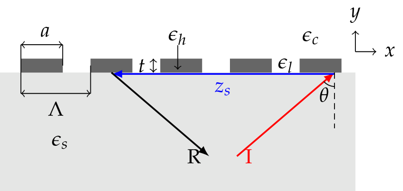
II Goos-Hänchen shift and frozen mode
When a Gaussian beam is totally reflected from a surface, the axis of the reflected beam experiences a lateral shift with respect to the position predicted by geometric optics[10]. Such a phenomenon is named after the discoverers Goos and Hänchen, and has been shown as an example of discrepancy between geometric optics and the wave nature of the light. The shift is related to the change of the reflection phase for different plane wave components of the incident beam. Mathematically, the Goos-Hänchen shift can be evaluated as[11]
| (1) |
where is the phase of the reflection coefficient of the plane wave component with a lateral wavenumber of . Here an time variation is assumed for the electromagnetic field. The Goos-Hänchen shift is usually positive for the reflection from an interface between two regular dielectrics, while negative on interfaces between regular dielectrics and plasmonic material or metamaterial.
The negative Goos-Hänchen shift has attracted a lot of research interest, one of which is to control the direction of energy flow in a dielectric slab waveguide with respect to the wave vector of the guided mode, as discussed in the same paper that proposed the trapped rainbow[1]. Whereas the original discussion was from a rather intuitive approach, here we would like to give a rigorous mathematical description. Considering a slab waveguide made of a dielectric of refractive index and thickness . A guided mode can be described as a plane wave total-internally reflected back and forth on the two interfaces that satisfies the following relationship:
| (2) |
where is the free space wavenumber, is the angle of incidence, , is the phase loss (the phase of the reflection coefficient) on the two side walls, respectively, while an integer. When written in terms of , the wavenumber parallel to the waveguide wall, we have
| (3) |
Take the total differential of both sides with respect to and , we get
| (4) |
which is a relationship a guided mode must satisfy in addition to (2). When deriving the former equation, we assume that does not change with frequency, which is a reasonable assumption for dielectric waveguides. Divide both sides by and take the limit of , we get
| (5) |
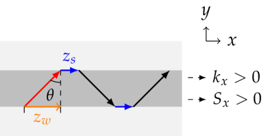
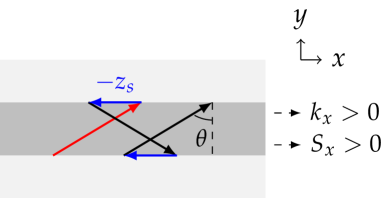
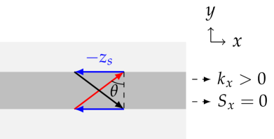
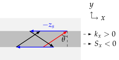
Notice that is always positive. This is because is the delay of the center of the Gaussian pulse at the reflection of the interface. For lossless reflection (which is the case here), this delay must be positive for a causal system. This means the sign of the right hand side completely determines the sign of , which is proportional to the group velocity. For the right hand side, the second term is the Goos-Hänchen shift on the two side walls. Also notice that . Thus, if we let , is actually the forward displacement of the ray when propagating from one side wall to the other (see Fig.1a). Combining the contribution of and together, the right hand side of (5) gives the total direction displacement of a ray in a round trip, as we see in Fig. 1. When the waveguide and the surrounding medium are both made of regular dielectrics, the Goos-Hänchen shift is positive, thus the right hand side is always positive. This means we always have . Things become interesting when we have negative Goos-Hänchen shift on one or both of the side walls, especially when it is of large magnitude so that the total displacement is negative (Fig. 1d). In this case, the group velocity would be negative, and the energy propagates anti-parallel to . When the Goos-Hänchen shift is just enough to make the right hand side goes to zero (the situation described by Fig. 1c), we have , and a “frozen mode” of the waveguide is formed. This is a guided mode with finite propagating constant, but zero net power propagation. All these conclusions are consistent with those in Ref.[1] but with rigorous mathematical analysis. We would like to point out that the conclusions only hold when the waveguide material has no temporal or spatial dispersion, i.e. and , as assumed when deriving (4). This is a reasonable assumption for dielectric waveguide, but not for metamaterial waveguides.
III Negative Goos-Hänchen shift and frozen mode on a dielectric grating
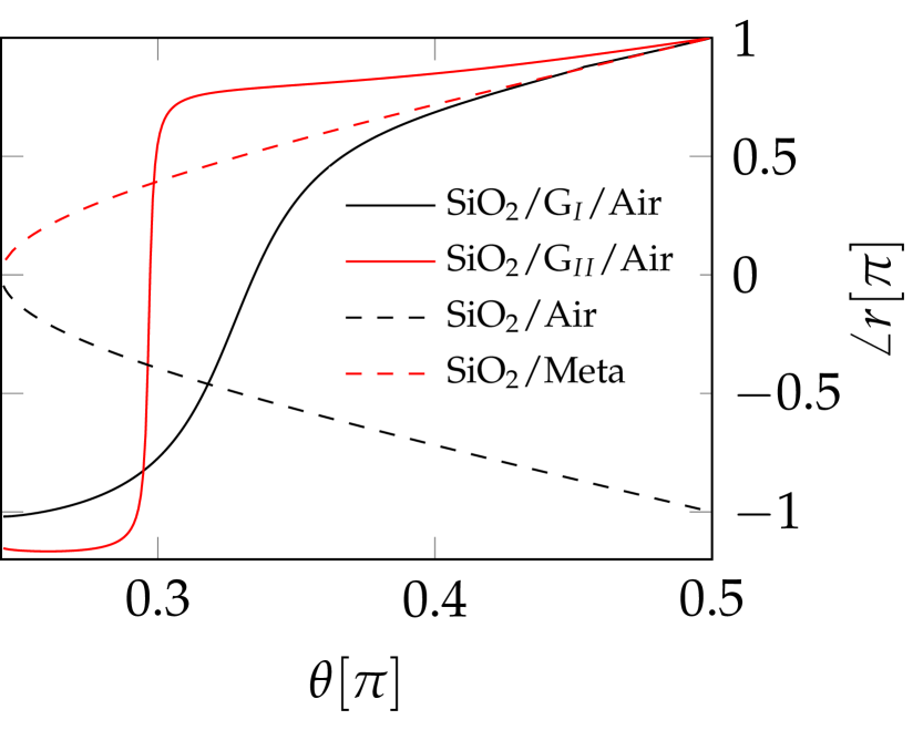
A negative Goos-Hänchen shift is crucial in building a frozen mode. This can be achieved on the surface of plasmonic materials or metamaterials, but is usually accompanied with large ohmic losses. However, it is possible to make negative Goos-Hänchen shift using completely dielectric devices, as we demonstrated in a recent publication[12]. The system under consideration is shown in Fig. 2a, where a thin grating made of Si is placed on a substrate of \ceSiO2. For certain grating design, the phase of the reflection coefficient for incidence from the \ceSiO2 side is of very different nature compared to that on the \ceSiO2/Air interface, as we see in Fig. 2b in which polarized incidence is studied, i.e. is the only electric field component. Whereas the phase decreases with the incident angle for a \ceSiO2/Air interface indicating a positive Goos-Hänchen shift (see --- in Fig. 2b), on the \ceSiO2/Grating interface, the phase increases, exhibiting a negative Goos-Hänchen shift (see — and — in Fig. 2b). This is similar to that of a \ceSiO2/Metamaterial case (see --- in Fig. 2b). The negative Goos-Hänchen shift is related to the guided mode of the grating. For the second band of the guided mode of the grating, the energy propagates to the opposite direction of the wave vector. The part of the dispersion curve for this band that is between the light lines of the free space and the substrate is leaky on the substrate side, and can couple to the incident beam efficiently. According to a commonly accepted explanation, the negative energy propagation with respect to the lateral wave propagating direction is responsible for the negative Goos-Hänchen shift[12, 13]. The amount of Goos-Hänchen shift can be controlled by the grating design: depending on the parameters of the grating, we may have a very large (a steep - curve) or a mediocre (a slow-varying - curve) Goos-Hänchen shift. In fact, the amount of Goos-Hänchen shift ranges from tens of nanometers up to several millimeters. In our study, a Goos-Hänchen shift of more than times of the free space wavelength[12] has been observed.
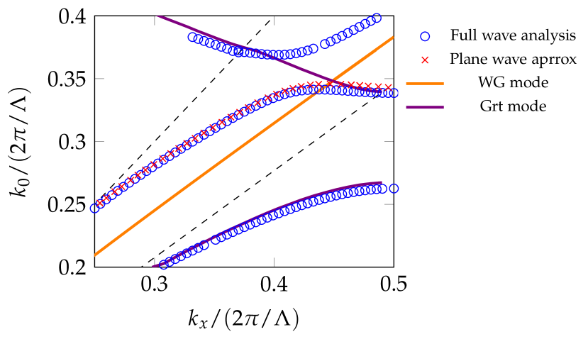
With the help of the negative Goos-Hänchen shift on the grating, we can readily realize the frozen mode discussed in the former section, by placing the grating on the sides of a dielectric waveguide. It turns out that grating on one side is enough to realize our goal. One of the designs makes use of a \ceSiO2 waveguide of thick and a grating of in thickness. To calculate the dispersion curve of this grating-decorated waveguide, we first find out the reflection phase on the \ceSiO2/Grating interface and the \ceSiO2/Air interface, respectively. These values are then used in (2) to get the dispersion relation. The results are shown in Fig. 3a as red cross. Notice how the dispersion curve bends to form a local extreme where goes to zero at which a frozen mode is formed. Calculation confirms that the right hand side of (5) indeed goes to zero at the top of the dispersion curve, which demonstrates the application of (5) in finding a frozen mode. The numerical evaluation also shows that the right hand side of (5) is positive for the part of the dispersion curve with smaller than that at the top point, and negative when is larger than that at the top. This is consistent with the positive or negative group velocity the dispersion curve shows (see Fig. 1). The nature of the negative Goos-Hänchen shift can be used to understand the frozen mode. Recall that the negative Goos-Hänchen shift is usually explained[13] by an energy flow beyond the reflection interface that is opposite to . If this power flow compensates completely the forward power flow inside the waveguide, no net power flow is carried by the guided mode, and a zero group velocity is expected.
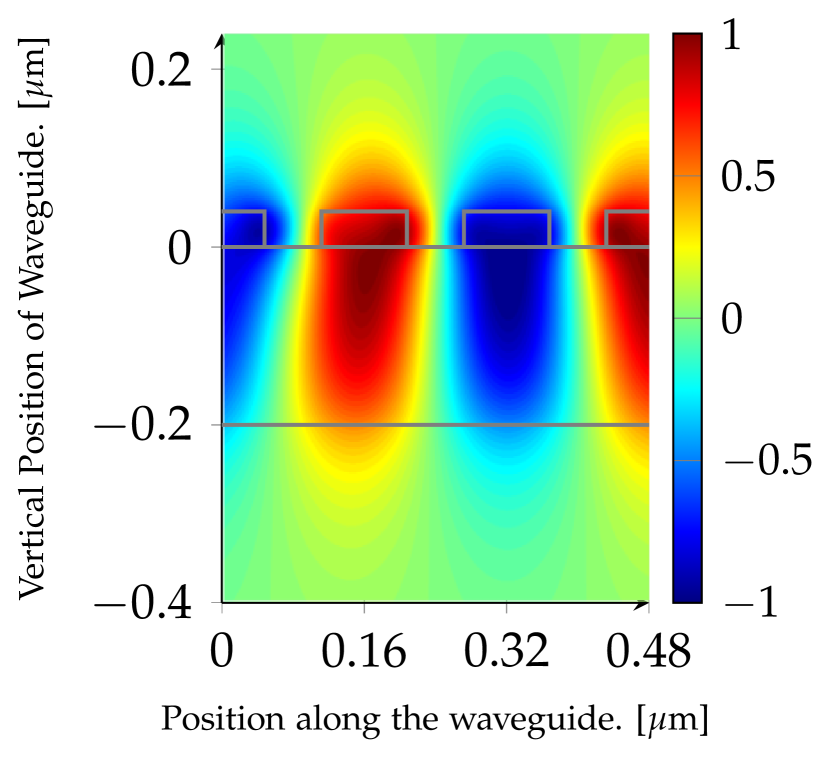
The evaluation of the dispersion relation using (2) ignores the high order spatial harmonics of the field around the grating, of course. To see if this poses any important influence, we also evaluated the dispersion relation of the waveguide using full wave analysis. To do this, we use MEEP, an open source numerical electromagnetic package based on the finite-difference, time-domain (FDTD) method. The result is shown as circles in the same plot of Fig. 3a, together with the guided modes of the same Si grating sitting on a \ceSiO2 substrate of infinite thickness. We can identify the nature of each part of the dispersion curve by examining the field distribution of the guided modes. For the lowest band below the light line of \ceSiO2, the electromagnetic field is well confined inside the grating, and the dispersion curve overlaps well with the guided mode of the grating on \ceSiO2 substrate. These modes are below the light line of \ceSiO2 and does not couple well with the propagating plane waves in the \ceSiO2 waveguide, thus can not be predicted by (2). Rather, this is the guided mode of the grating itself. The second band is above the light line of \ceSiO2, thus the plane waves inside the \ceSiO2 slab waveguide take part in the formation of this band. Notice that the dispersion curve calculated from (2) (plotted as ) indeed overlaps well with that calculated from full-wave analysis. This means the high order spatial harmonics of the field do not contribute obviously in forming the mode, and to use (2) for mode calculation is safe. The shape of the lower part of the second band is similar to the dispersion curve of a bare \ceSiO2 slab waveguide of the same thickness, but shifted in because of the changed reflection phase on the \ceSiO2/grating wall (see (2)). As the frequency increases, the waveguide mode gets close to the second band of the grating’s guided mode where the two anti-cross each other, causing the opening of a bandgap. Notice that, the second band of the grating mode is also where negative Goos-Hänchen shift is observed[12]. The instantaneous field distribution of the frozen mode, i.e. the mode at the top of the lower band, is shown in Fig. 3b. The Poynting vector evaluated from these simulation results indeed confirm the zero net power flow of this mode.
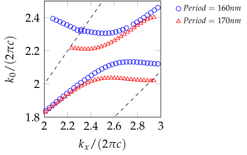
One important feature needed for a trapped rainbow is the capability to tune the frequency of the frozen mode. In the original paper of trapped rainbow[1], this is realized by varying the thickness of the waveguide. A tapered waveguide requires gray-scale etching, which is difficult in the conventional micro- and nano- fabrication developed for planar geometry. The grating used in our device can tune the operating frequency without thickness variation: we can change the lateral design parameters (the period and the duty cycle ) to modulate the frequency of the frozen mode while leaving the waveguide thickness untouched. It appears that the frozen mode frequency can be varied most effectively by changing the period. The effect is shown in Fig. 4, in which the dispersion curves for two waveguides of the same \ceSiO2 slab and grating thickness ( and , respectively) but different grating periods ( : ; : .) The result in this plot is again from MEEP simulation. As we can see, the frequency of the frozen mode (the top of the lower band) is obviously changed. For a period variation of , the frequency is changed by .
IV Trapped Rainbow
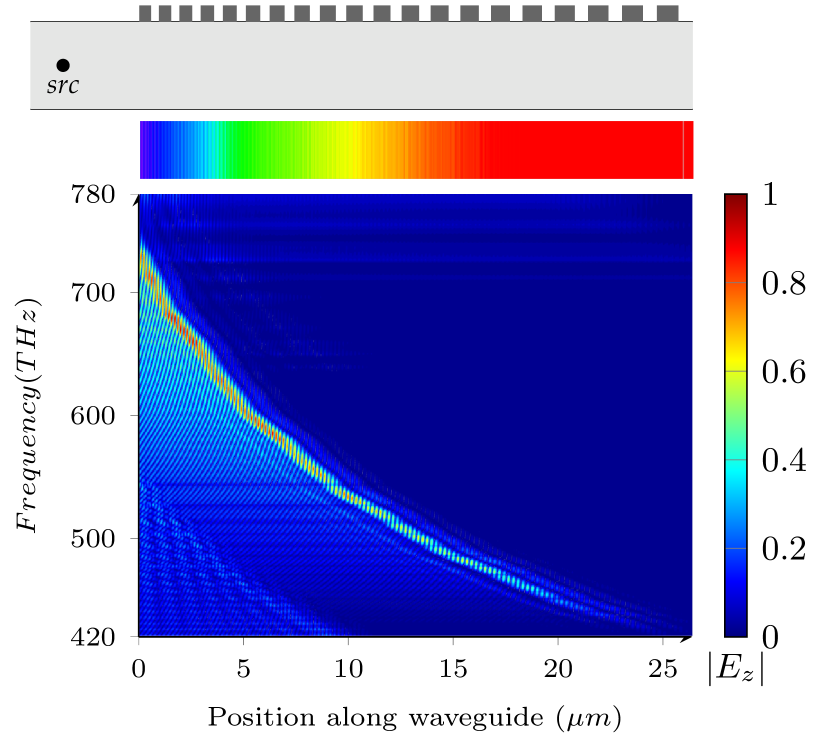
To construct a trapped rainbow requires building a waveguide on which the frozen mode is of different frequency at different position along the device. In our design, this is realized by placing multiple segments of the waveguide of different grating period one after another. A schematic is shown in the top of Fig. 5a. As a demonstration, our first device is composed of waveguide segments, and the grating of each segment consists of 10 identical periods. These gratings have the same thickness of and duty cycle , but the period varies from to . The free-space wavelength of the frozen mode that would be supported by waveguides of these different designs range from to . The device is fed from the left by a slab waveguide made of the same material and of the same thickness. A broad band pulse is launched in the feeding waveguide, and incident to the trapping device from the left. ” We arrange the waveguide segments so that the frozen mode frequency decreases from left to the right, with the segments of higher frequency sitting at the upper stream of the optical power flow. This is because, according to Fig. 3a and Fig. 4, each segment actually supports two modes of zero group velocity, one at the top of the lower band while the other at the bottom of the top band. In our design, we use the lower band of every segment, and the arrangement described above promises that the bottom of the upper band of each segment falls inside the bandgap of its neighboring upper stream segment, thus would not be excited. The structure is again simulated in MEEP. In the simulation, we record the field at different positions along the center of the waveguide after the transient field fades out. A Fourier transform then reveals the spectrum at each position. The observed spectrum intensity at different positions along the whole device is shown in the bottom of Fig. 5a. Here the horizontal axis is the lateral position along the device with the origin at the beginning of the first waveguide, while the vertical axis is the signal frequency. The color shows the spectrum intensity. In the simulation, a pulse signal with approximately flat spectrum in the band of interests is used, so that no frequency component has an advantage in the power intensity. As we walk from left to the right along the device, we can indeed observe 14 discrete steps in the spectrum at positions corresponding to the 14 waveguide segments (the last one is less obvious due to the reflection by the segments ahead of it), going from (violet color) to (red color). To give an intuitive understanding to the result, we show the color that would be observed at different positions along the device rendered from the spectrum measured at the very position. The algorithm to render a color from a distribution of spectrum intensity is discussed in Ref.[14], and the result is shown in the middle of Fig. 5a. The result clearly gives a “rainbow” trapped along the device. The color shows the spectrum intensity. In the simulation, a pulse signal with approximately flat spectrum in the band of interests is used, so that no frequency component has an advantage in the power intensity. As we walk from left to the right along the device, we can indeed observe 14 discrete steps in the spectrum at positions corresponding to the 14 waveguide segments (the last one is less obvious due to the reflection by the segments ahead of it), going from (violet color) to (red color). To give an intuitive understanding to the result, we show the color that would be observed at different positions along the device rendered from the spectrum measured at the very position. The algorithm to render a color from a distribution of spectrum intensity is discussed in Ref.[14], and the result is shown in the middle of Fig. 5a. The result clearly gives a “rainbow” trapped along the device.

The former demonstration uses a piecewise continuous design. To have a rainbow with adiabatic color change, we turn to a device with tapered design. Rather than physically tapering the thickness of the slab waveguide, we use continuously changed grating period along the whole device in the same range as the former example, as we see in the schematic shown on the top of Fig. 5b. A similar idea was used to make flat focusing lens in one of the authors’ former works[15]. We expect the result to be a smooth-out version of the trapped rainbow shown in Fig. 5a. The result indeed proves our expectation (refer to the middle of Fig. 5b). As we see in the bottom of Fig. 5b, the peak frequency of the spectrum changes as the observation position changes, and a rainbow of continuously varying color can be observed.
V Conclusion
In this paper we make use of the negative Goos-Hänchen shift on the surface of a dielectric grating to realize a frozen mode, i.e. a guided mode on a waveguide with no net power propagation. Further, by tuning the design parameters of the grating on a waveguide, we can achieve frozen modes with different frequencies sitting at different positions along the waveguide, so that a broad band pulse covering the whole visible spectrum can be caught by the waveguide, with different frequency components stored at different positions. The current design is, to the best of our knowledge, the first demonstration of the “trapped rainbow” proposed in [1] that make explicit use of the negative Goos-Hänchen shift, the mechanism originally proposed in that paper. At the same time, the use of only dielectric materials promises a much lower ohmic loss. The negative Goos-Hänchen shift is realized on the surface of a grating, which has a geometry much easier to be fabricated compared to the usually three dimensional structure of a metamaterial. Tuning the lateral design parameters rather than the thickness further reduces the fabrication difficulty. All these features make the device suitable for practical use in areas such as slow light.
We should point out that the “trapped rainbow” serves as a manifesto of the capability of the grating in controlling the dispersion property of a slab waveguide. According to (5), the Goos-Hänchen shift, or more generally, the reflection phase on the surface of the grating, directly determines the behavior of the group velocity. Since the reflection phase is controlled by the design parameters of the grating, (5) gives us a straightforward method to synthesize the dispersion property of the waveguide as needed. We believe this dispersion engineering approach can have promising applications in optical networks.
References
- [1] K. L. Tsakmakidis, A. D. Boardman, and O. Hess, ““trapped rainbow” storage of light in metamaterials,” Nature 450, 397–401 (2007).
- [2] L. V. Hau, S. E. Harris, Z. Dutton, and C. H. Behroozi, “Light speed reduction to 17 metres per second in an ultracold atomic gas,” Nature 397, 594–598 (1999).
- [3] P. S. Ma, Y. E. Kwon, and Y. Y. Kim, “Wave dispersion tailoring in an elastic waveguide by phononic crystals,” Applied Physics Letters 103, 151901 (2013).
- [4] J. Li, T. P. White, L. O’Faolain, A. Gomez-Iglesias, and T. F. Krauss, “Systematic design of flat band slow light in photonic crystal waveguides,” Optics Express 16, 6227–6232 (2008).
- [5] S. A. Schulz, L. O’Faolain, D. M. Beggs, T. P. White, A. Melloni, and T. F. Krauss, “Dispersion engineered slow light in photonic crystals: a comparison,” Journal of Optics 12, 104004 (2010).
- [6] P. Colman, S. Combriè, G. Lehoucq, and A. De Rossi, “Control of dispersion in photonic crystal waveguides using group symmetry theory,” Optics Express 20, 13108–13114 (2012).
- [7] Q. Gan, Y. Gao, K. Wagner, D. Vezenov, Y. J. Ding, and F. J. Bartoli, “Experimental verification of the rainbow trapping effect in adiabatic plasmonic gratings,” Proceedings of the National Academy of Sciences 108, 5169–5173 (2011).
- [8] Q. Gan and F. J. Bartoli, “Surface dispersion engineering of planar plasmonic chirped grating for complete visible rainbow trapping,” Applied Physics Letters 98, 251103 (2011).
- [9] V. N. Smolyaninova, I. I. Smolyaninov, A. V. Kildishev, and V. M. Shalaev, “Experimental observation of the trapped rainbow,” Applied Physics Letters 96, 211121 (2010).
- [10] F. Goos and H. Hänchen, “Ein neuer und fundamentaler versuch zur totalreflexion,” Annalen der Physik 436, 333?346 (1947).
- [11] T. Tamir and E. Garmire, Integrated optics (Springer-Verlag, Berlin; New York, 1979).
- [12] R. Yang, W. Zhu, and J. Li, “Giant positive and negative goos-hänchen shift on dielectric gratings caused by guided mode resonance,” Optics Express 22, 2043–2050 (2014).
- [13] R. RENARD, “Total reflection: A new evaluation of the goos-hänchen shift,” J. Opt. Soc. Am. 54, 1190–1196 (1964).
- [14] see http://www.fourmilab.ch/documents/specrend/.
- [15] D. Fattal, J. Li, Z. Peng, M. Fiorentino, and R. Beausoleil, “Flat dielectric grating reflectors with focusing abilities,” Nature Photonics 4, 466–470 (2010).