Near Unity Optical Spin Polarization in GaSe Nanoslabs
Abstract
We report nearly complete preservation of “spin memory” between optical absorption and photoluminescence (PL) in nanometer slabs of GaSe pumped with 0.2 eV excess energy. At cryogenic temperatures, the initial degree of circular polarization () of PL approaches unity, with the major fraction of the spin polarization decaying with a time constant 500 ps in sub-100-nm GaSe nanoslabs. Even at room temperature, as large as 0.7 is observed, while pumping 1 eV above the band edge yields = 0.15. Angular momentum preservation for both electrons and holes is due to the separation of the non-degenerate conduction and valence bands from other bands. In contrast to valley polarization in atomically thin transition metal dichalcogenides, here optical spin polarization is preserved in nanoslabs of 100 layers or more of GaSe.
pacs:
72.25.Fe,72.25.Rb,71.35.CcSolid-state systems exhibiting high spin polarization and long spin relaxation time are desirable for spintronic applications. Various semiconductors have been studied for creation of long-lived non-equilibrium spin populations and coherences Dyakonov and Perel (1984); Zutic et al. (2004); Dyakonov (2008); Awschalom et al. (2013). The most extensively studied system is gallium arsenide (GaAs). However, optically pumped electron spin polarization is limited to 1/2, while the maximal degree of circular polarization of photoluminescence is 1/4 Dyakonov and Perel (1984); Dyakonov (2008), owing to the degenerate heavy- and light-hole valence bands and sub-ps hole spin relaxation. Doping Kikkawa et al. (1997) or quantum confinement Ohno et al. (1999) has been used to quench electron spin relaxation. Unity electron spin polarization can be achieved in heterostructures where heavy- and light-hole energy degeneracy is lifted by quantum confinement or strain. Still, near-resonant optical excitation is necessary to avoid transitions involving both heavy- and light-hole bands. In analogy to spin polarization, valley polarization has been demonstrated in monolayer transition metal dichalcogenides (TMDs) with potential applications exploiting both spin and valley degrees of freedom.In monolayer TMDs with broken inversion symmetry, a direct gap emerges at the corners ( points) of the Brillouin zone, enabling valley-dependent inter-band transitions under circularly polarized optical excitation Yao et al. (2008); Cao et al. (2012); Zeng et al. (2012). Furthermore, the substantial spin-splitting of valence bands at the band edges due to spin-orbit interaction originating from the orbitals of TM ions has led to recent reports of long hole spin and valley lifetimes Xiao et al. (2012); Mak et al. (2012), valley exciton polarization and coherence Xu et al. (2014); Zhu et al. (2014), circularly polarized electroluminescence Zhang et al. (2014), and valley Hall effect Mak et al. (2014). Indeed, circularly polarized PL was observed in single- and bi-layer TMDs Cao et al. (2012); Zeng et al. (2012); Mak et al. (2012); Xu et al. (2014); Zhu et al. (2014) with steady-state near-resonant circularly polarized excitation. However, time- and polarization-resolved PL measurements suggest that, at least in \ceMoS2, circularly polarized PL can result from sub-10-ps recombination and valley (spin) lifetimes rather than an intrinsically long-lived valley or hole spin polarization Cao et al. (2012); Lagarde et al. (2014); Glazov et al. (2014). Additionally, emission at the direct gap becomes dominant only at the monolayer level Splendiani et al. (2010); Mak et al. (2010); Tonndorf et al. (2013).
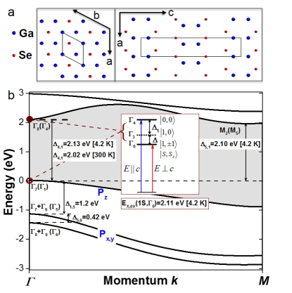
Here, we demonstrate GaSe as a promising material for generating and preserving a high degree of spin polarization. The unique bandstructure (Fig. 1) of the group-III monochalcogenides removes degeneracies between orbital states and thereby allows generation and preservation of a high degree of spin polarization Gamarts et al. (1977); Ivchenko et al. (1977). We investigate the photoluminescence of excitons in sub-100-nm to 1000-nm thick GaSe slabs (nanoslabs) under non-resonant circularly polarized optical excitation. Polarized time-dependent PL in GaSe reveals a high initial degree of circular polarization when excited with excess energy from about 0.1 to 0.2 eV. High is indicative of spin preservation of optically active carriers during the optical absorption-cooling process. Unlike TMDs, GaSe has a quasi-direct gap in the bulk form Mooser and Schlüter (1973); Capozzi et al. (1993), making it a potentially versatile material in which strong emission occurs and light-matter coupling can be controlled from bulk to nanoscale thicknesses.
The physical properties of \ceGaSe are largely determined by those of a single layer (Fig. 1) due to the high electron density within the layer and weak interlayer interaction Mooser and Schlüter (1973); Schlüter et al. (1976). The Se-Ga bond tilts 29∘ out of the layer plane so that Se 4 electrons experience much greater Coulomb attraction with \ceGa cations than Se 4 electrons do. This results in a large negative crystal field ( -1.4 eV) compared to wurtzite-type materials ( +0.05 eV) so that the Se 4 states lie 1.2 and 1.6 eV below the Se 4 state (Fig. 1b). Consequently, near the point () only light with can excite dipole transitions between the -like uppermost valence band and -like lowest conduction band. Experimentally, the absorption coefficient for is about cm-1, a factor of 30 smaller than for Le Toullec et al. (1977). The transition for is weakly dipole-allowed owing to band mixing induced by strong spin-orbit interaction ( 0.44 eV) and weak interlayer coupling. The optical pumping and selection rules near are best understood in an exciton (two-particle) picture [binding energy 20-30 meV] Mooser and Schlüter (1973) as detailed in Supplementary Information. The essential feature is that the lowest states correspond to total exciton spin with -component and can be excited by light with wave vector (). We have exploited these selection rules to investigate the spin dynamics of GaSe under non-resonant circularly polarized optical excitation as a function of slab thickness .
Time- and polarization-resolved PL measurements (see Methods) allow us to separately determine the recombination time, the initial spin orientation, and the spin relaxation time. Polarization-resolved PL measurements are performed under excitation with energy about 0.1 to 0.2 eV above the GaSe band gap. The band-edge exciton PL emission at room temperature is near 620 nm (2.0 eV), independent of thickness, under 594 nm (2.087 eV) excitation. Additionally, we observe that the quantum yield of luminescence is greatly suppressed in sub-50-nm thick samples (Supplementary Fig. S2). In this paper, we focus on GaSe nanoslabs ranging from about 90 to 2000 nm thick.
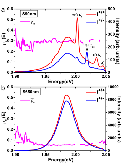

Upon absorption of circularly polarized light above the band-gap, the stationary (time-averaged) degree of circular polarization () of luminescence represents photoexcited carrier spin memory. In Fig. 2, we show the polarized time-integrated PL spectra [] for two samples of thickness of 90 nm and 650 nm at room temperature. Across a range of sample thicknesses (), time-integrated PL shows a pronounced increase of from 0.05 in bulk to 0.3 in sub-100-nm nanoslabs. Corresponding polarized time-dependent PL are shown in Fig. 3a-b. The degree of circular polarization decays within 10 ps, independent of the slab thickness and photoexcited carrier density. In contrast, the total (unpolarized) PL decays exponentially with a time constant () that increases linearly with thickness from about 20 ps to 250 ps for 90 nm 700 nm (Fig 3c). The fast PL rise and decay time constants in sub-100-nm GaSe nanoslabs are comparable to the 10-ps spin relaxation time, resulting in the preservation of a high spin polarization during the brief absorption-cooling-emission cycle Nüsse et al. (1997). In Fig. 3d, we plot as a function of PL decay time for all samples studied. The stationary is well described by a simple model: , where is the lifetime of photoexcited carriers, and is the spin relaxation time. Fitting yields and ps, consistent with the time-resolved measurements. Therefore, the apparent enhancement of “spin memory” revealed in time-integrated PL is largely owing to a linear decrease of the PL decay time () with thickness.
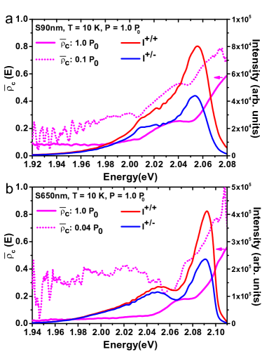
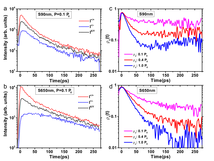
At cryogenic temperature (T = 10 K), the spin and PL decay dynamics with 560-nm (2.214) to 575-nm (2.156 eV) excitation slow markedly. For both 90-nm and 650-nm samples, the stationary surpasses 0.8 (approaching 1 at low photoexcited density) at the high-energy range of the exciton emission spectrum and decreases gradually to about 0.3 at low emission energies (Fig. 4 and Supplementary Fig. S3 & S4). Similar is observed for all samples (not shown). Meanwhile, time-dependent PL decay becomes bi-exponential with time constants 20-50 ps and 150-200 ps (Fig. 5a-b) in all samples. In contrast, the PL rise time remains ps, suggesting that the cooling and momentum relaxation of radiative photoexcited carriers are independent of temperature. Finally, time-dependent circular polarization is also found to be bi-exponential, with decay time constants 30-40 ps and 500 ps (Fig. 5c-d). Assuming a high spin relaxation rate of non-thermal carriers during the cooling process, we reproduce quantitatively the bi-exponential decays of both PL intensity and polarization using a rate-equation model Vinattieri et al. (1994) (see Supplementary Information). The shorter time constant shows a weak power-law dependence on the photoexcited density () with , while there is no identifiable dependence on thickness for either population decay or spin relaxation.
To explore the limits of spin memory, we also performed experiments on the 650 nm sample under 3.0 eV excitation (Supplementary Fig. S5). We find that the initial at the band edge is 0.15, irrespective of temperature. The reduction of with increasing carrier density and with increasing excitation energy suggest that the Elliot-Yafet (EY) mechanism plays a larger role than the Dyakonov-Perel (DP) mechanism Dyakonov and Perel (1984); Pikus and Titkov (1984); Wu et al. (2010) in the initial spin relaxation for non-thermal carriers at low temperature.
The generation of a substantial degree of spin polarization at the band edge after highly non-resonant excitation is a consequence of (1) a large degree of spin polarization of the initially created high-energy carriers and (2) spin relaxation rates that are slow compared to energy and momentum relaxation as well as the band-edge PL decay rates. All samples display a nearly instantaneous rise (5 ps, resolution-limited) in the band-edge PL under excitation at excess energies 300 meV at room and cryogenic temperatures, indicating sub-10-ps momentum and energy relaxation of photoexcited carriers toward =0 ( point). This time scale is consistent with the momentum scattering time of 5 ps deduced by Gamarts et al. Gamarts et al. (1977); Ivchenko et al. (1977). Carriers thus spend limited time in high-momentum states where spin relaxation is fastest. In contrast, at 3.0 eV excitation, carriers take markedly longer to dissipate 1 eV excess energy, especially at T = 10 K. This increase of energy relaxation time partially accounts for the reduced initial degree of spin polarization observed under 3.0 eV excitation.
The decrease of PL decay with thickness for 700 nm at K means that a greater fraction of the emission occurs before the spin polarization decays, leading to larger in sub-100-nm GaSe nanoslabs. The decrease of is unlikely due to an enhancement of radiative recombination rates with dimensionality and confinement Andreani et al. (1991) given that the bulk Bohr exciton radius of GaSe is only 5 nm. The linear dependence of can result from the propagation of exciton-polaritons Aaviksoo (1991) or non-radiative surface recombination Aspnes (1983) (see Supplementary Information). The PL measurements presented here only probe excitons and carriers near the point. Nonetheless, the distinct PL dynamics at room and cryogenic temperatures suggest that there is significant non-radiative recombination due to inter-valley scattering between the and M valleys Capozzi et al. (1993).
The reduced mixing of valence bands makes GaSe and other group-III monochalcogenides such as GaS and InSe Kuroda et al. (1980) promising materials for devices relying on the ability to generate and maintain high degrees of spin polarization. In these materials, the hole spin relaxation rate is expected to decrease significantly compared to that in III-V semiconductors because the EY relaxation mechanism is suppressed by the reduced mixing of distant valence bands. This hypothesis is supported by the quantitative exciton and spin relaxation rates obtained by fitting the experimental polarized PL dynamics as described in Supplementary Information. Nanoscale multi-layer GaSe or InSe are, in principle, less challenging to synthesize and integrate with micro- and nano-fabrication processes compared to atomic membranes of TMDs. Additionally, non-centrosymmetric group-III monochalcogenides allow for more direct optical control of light-matter coupling beyond the monolayer regime.
Methods
Sample growth and characterization. GaSe single crystals are grown from stoichiometric amounts of high purity (7N) precursors using the vertical Bridgman method Mandal et al. (2008). X-ray powder diffraction results confirmed the hexagonal -GaSe structure with = 3.743 and = 15.916 . Inductively coupled plasma emission mass spectroscopy (ICPMS) was carried out to determine the stoichiometry of these samples. These GaSe samples are stoichiometric with 50.001% Ga (atomic) and 49.997% Se (atomic).
Sample preparation. Like graphene/graphite and layered transition metal dichalcogenides, GaSe can be mechanically exfoliated into atomically thin few-layer crystals. Atomically thin and nanometer thick GaSe crystals are mechanically exfoliated from a Bridgman-grown crystal and deposited onto a silicon substrate with a 90 nm \ceSiO2 layer. Sample thickness is measured by atomic force microscopy (Supplementary Fig. S1). Samples are mounted in vacuum on a copper cold finger attached to an optical liquid helium flow cryostat for all experiments.
Optical pumping. GaSe nanoslabs are optically excited by a 2-ps pulsed laser with a varying central wavelength between 560 to 610 nm from a synchronously pumped optical parametric oscillator. The laser beam is focused through a microscope objective (numerical aperture N.A. = 0.28) to an area of about 80 m2 on the sample. The wave vector of the pump is along the crystal -axis (the surface normal), i.e. the electric field vector is orthogonal to the -axis (). The maximum deviation from normal incidence is 8∘ in air and in the crystal for this objective. The polarization and pump flux () of the pump laser is controlled by liquid-crystal-based devices without mechanical moving parts. We estimate the photoexcitation density to be from cm-3 to cm-3 ( cm-2 per layer) considering the absorption coefficient at 2.1 eV ( cm-1 for ) and Fresnel loss from reflection. The photoexcited carrier density is below the Mott transition Pavesi et al. (1989); Capozzi et al. (1993) of direct excitons occurring near e-h pair densities of cm-3.
Time-integrated and time-resolved photoluminescence spectroscopy. We characterize decays of optically excited carrier by measuring reflected photoluminescence (PL) propagating along the -axis through a standard microscopy set-up. PL spectra are observed using an imaging spectrometer (linear dispersion 1 nm/mm, focal length 750 mm, grating 300 grooves/mm) equipped with a liquid-nitrogen cooled CCD. To characterize the temporal evolution of the exciton/carrier population, we monitored time-dependent photoluminescence near the band edge using a streak camera system.
Polarized time-dependent photoluminescence. To better understand the spin relaxation of photoexcited excitons (electrons/holes) in GaSe crystalline nanoslabs, we analyzed time-dependent polarization properties of PL under nonresonant circularly and linearly polarized 2-ps pulsed pump. The spin-lattice relaxation time of the photoexcited carriers can be determined from co-circularly and cross-circularly polarized time-dependent PL.
References
- Dyakonov and Perel (1984) M. I. Dyakonov and V. I. Perel, “Theory of optical spin orientation of electrons and nuclei in semiconductors,” in Optical Orientation, Vol. 8 (Elsevier, 1984) pp. 11–72.
- Zutic et al. (2004) I. Zutic, J. Fabian, and S. Das Sarma, “Spintronics: Fundamentals and applications,” Rev. Mod. Phys. 76, 323–410 (2004).
- Dyakonov (2008) M. I. Dyakonov, ed., Spin Physics in Semiconductors, Springer Series in Solid-State Science, Vol. 157 (Springer, 2008).
- Awschalom et al. (2013) D. D. Awschalom, L. C. Bassett, A. S. Dzurak, E. L. Hu, and J. R. Petta, “Quantum spintronics: engineering and manipulating atom-like spins in semiconductors.” Science 339, 1174–9 (2013).
- Kikkawa et al. (1997) J. M. Kikkawa, I. P. Smorchkova, N. Samarth, and D. D. Awschalom, “Room-temperature spin memory in two-dimensional electron gases,” Science 277, 1284–1287 (1997).
- Ohno et al. (1999) Y. Ohno, R. Terauchi, T. Adachi, F. Matsukura, and H. Ohno, “Spin relaxation in GaAs(110) quantum wells,” Phys. Rev. Lett. 83, 4196–4199 (1999).
- Yao et al. (2008) W. Yao, D. Xiao, and Q. Niu, “Valley-dependent optoelectronics from inversion symmetry breaking,” Phys. Rev. B 77, 235406 (2008).
- Cao et al. (2012) T. Cao, G. Wang, W. Han, H. Ye, C. Zhu, J. Shi, Q. Niu, P. Tan, E. Wang, B. Liu, and J. Feng, “Valley-selective circular dichroism of monolayer molybdenum disulphide,” Nature Commun. 3, 887 (2012).
- Zeng et al. (2012) H. Zeng, J. Dai, W. Yao, D. Xiao, and X. Cui, “Valley polarization in MoS2 monolayers by optical pumping,” Nature Nanotech. 7, 490 (2012).
- Xiao et al. (2012) D. Xiao, G-B . B. Liu, W. Feng, X. Xu, and W. Yao, “Coupled spin and valley physics in monolayers of MoS2 and other group-VI dichalcogenides,” Phys. Rev. Lett. 108, 196802 (2012).
- Mak et al. (2012) K. F. Mak, K. He, J. Shan, and T. F. Heinz, “Control of valley polarization in monolayer MoS2 by optical helicity,” Nature Nanotech. 7, 494 (2012).
- Xu et al. (2014) X. Xu, W. Yao, D. Xiao, and T. F. Heinz, “Spin and pseudospins in layered transition metal dichalcogenides,” Nature Phys. 10, 343 (2014).
- Zhu et al. (2014) B. Zhu, H. Zeng, J. Dai, Z. Gong, and X. Cui, “Anomalously robust valley polarization and valley coherence in bilayer WS2,” Proc. Natl. Acad. Sci. U.S.A. 111, 11606–11611 (2014).
- Zhang et al. (2014) Y. J. Zhang, T. Oka, R. Suzuki, J. T. Ye, and Y. Iwasa, “Electrically switchable chiral light-emitting transistor,” Science 344, 725–728 (2014).
- Mak et al. (2014) K. F. Mak, K. L. McGill, J. Park, and P. L. McEuen, “The valley Hall effect in MoS2 transistors,” Science 344, 1489–1492 (2014).
- Lagarde et al. (2014) D. Lagarde, L. Bouet, X. Marie, C. R. Zhu, B. L. Liu, T. Amand, P. H. Tan, and B. Urbaszek, “Carrier and polarization dynamics in monolayer MoS2,” Phys. Rev. Lett. 112, 047401 (2014).
- Glazov et al. (2014) M. M. Glazov, T. Amand, X. Marie, D. Lagarde, L. Bouet, and B. Urbaszek, “Exciton fine structure and spin decoherence in monolayers of transition metal dichalcogenides,” Phys. Rev. B 89, 201302 (2014).
- Splendiani et al. (2010) A. Splendiani, L. Sun, Y. B. Zhang, T. S. Li, J. Kim, C. Y. Chim, G. Galli, and F. Wang, “Emerging photoluminescence in monolayer MoS2,” Nano Lett. 10, 1271–1275 (2010).
- Mak et al. (2010) K. Mak, C. Lee, J. Hone, J. Shan, and T. F. Heinz, “Atomically thin MoS2: A new direct-gap semiconductor,” Phys. Rev. Lett. 105, 136805 (2010).
- Tonndorf et al. (2013) P. Tonndorf, R. Schmidt, P. Böttger, X. Zhang, J. Börner, A. Liebig, M. Albrecht, C. Kloc, O. Gordan, D. R. T. Zahn, S. M. de Vasconcellos, and R. Bratschitsch, “Photoluminescence emission and Raman response of monolayer MoS2, MoSe2, and WSe2,” Opt. Express 21, 4908–4916 (2013).
- Gamarts et al. (1977) E. M. Gamarts, E. L. Ivchenko, M. I. Karaman, V. P. Mushinskii, G. E. Pikus, B. S. Razbirin, and A. N. Starukhin, “Optical orientation and alignment of free excitons in GaSe during resonance excitation. experiment,” Sov. Phys. JETP 46, 590 (1977).
- Ivchenko et al. (1977) E. L. Ivchenko, G. E. Pikus, B. S. Razbirin, and A. I. Starukhin, “Optical orientation and alignment of free excitons in GaSe under resonant excitation. theory.” Sov. Phys. JETP 45, 1172–1180 (1977).
- Mooser and Schlüter (1973) E. Mooser and M. Schlüter, “The band-gap excitons in gallium selenide,” Nuovo Cimento B 18, 164–208 (1973).
- Capozzi et al. (1993) V. Capozzi, L. Pavesi, and J. L. Staehli, “Exciton-carrier scattering in gallium selenide,” Phys. Rev. B. 47, 6340–6349 (1993).
- Schlüter et al. (1976) M. Schlüter, J. Camassel, S. Kohn, J. P. Voitchovsky, Y. R. Shen, and Marvin L. Cohen, “Optical properties of GaSe and GaSxSe1-x mixed crystals,” Phys. Rev. B 13, 3534–3547 (1976).
- Le Toullec et al. (1977) R. Le Toullec, N. Piccioli, M. Mejatty, and M. Balkanski, “Optical constants of -GaSe,” Nuovo Cimento B 38, 159–167 (1977).
- Nüsse et al. (1997) S. Nüsse, P. Haring Bolivar, H. Kurz, V. Klimov, and F. Levy, “Carrier cooling and exciton formation in GaSe,” Phys. Rev. B 56, 4578–4583 (1997).
- Vinattieri et al. (1994) A. Vinattieri, J. Shah, T. C. Damen, D. S. Kim, L. N. Pfeiffer, M. Z. Maialle, and L. J. Sham, “Exciton dynamics in GaAs quantum wells under resonant excitation,” Phys. Rev. B 50, 10868 (1994).
- Pikus and Titkov (1984) G. E. Pikus and A. N. Titkov, “Spin relaxation under optical orientation in semiconductors,” in Optical Orientation, Vol. 8 (Elsevier, 1984) pp. 73–131.
- Wu et al. (2010) M. W. Wu, J. H. Jiang, and M. Q. Weng, “Spin dynamics in semiconductors,” Phys. Rep. 493, 61 – 236 (2010).
- Andreani et al. (1991) L. C. Andreani, F. Tassone, and F. Bassani, “Radiative lifetime of free excitons in quantum wells,” Solid State Commun. 77, 641–645 (1991).
- Aaviksoo (1991) J. Aaviksoo, “Time-resolved studies of excitonic polaritons,” J. Lumin. 48 & 49, 57 – 66 (1991).
- Aspnes (1983) D. E. Aspnes, “Recombination at semiconductor surfaces and interfaces,” Surf. Sci. 132, 406–421 (1983).
- Kuroda et al. (1980) N. Kuroda, I. Munakata, and Y. Nishina, “Exciton transitions from spin-orbit split off valence bands in layer compound InSe,” Solid State Commun. 33, 687 – 691 (1980).
- Mandal et al. (2008) K. C. Mandal, A. Mertiri, G. W. Pabst, R. G. Roy, Y. Cui, P. Battacharya, M. Groza, A. Burger, A. M. Conway, and R. J. Nikolic, “Layered III-VI chalcogenide semiconductor crystals for radiation detectors,” in Proc. SPIE, Vol. 7079 (2008) p. 70790O.
- Pavesi et al. (1989) L. Pavesi, J. L. Staehli, and V. Capozzi, “Mott transition of the excitons in GaSe,” Phys. Rev. B 39, 10982–10994 (1989).
Acknowledgments
This work is supported by Michigan State University and by NSF through DMR-09055944. This research has made use of the W. M. Keck Microfabrication Facility. We thank Dat Do, Brage Golding, Bhanu Mahanti, and Carlo Piermarocchi for comments and discussions.
Author contributions
Y.T. led the optical measurements and data analysis, assisted by W. X.. K.M. grew the materials. C.W.L. conceived the project and developed the theoretical model. J.A.M. and C.W.L. supervised the project and wrote the paper with input from all authors.