Role Played by Surface Plasmons on Plasma Instability in Composite Layered Structures

Godfrey Gumbs1,2, Andrii Iurov1111E-mail contact: theorist.physics@gmail.com and Danhong Huang3 1Department of Physics and Astronomy, Hunter College of the City University of New York, 695 Park Avenue, New York, NY 10065, USA
2 Donostia International Physics Center (DIPC), P de Manuel Lardizabal, 4, 20018 San Sebastian, Basque Country, Spain
3Air Force Research Laboratory, Space Vehicles Directorate, Kirtland Air Force Base, NM 87117, USA
Abstract

We demonstrate the engineering of a source of radiation from growing surface plasmons (charge density oscillations) in a composite nano-system. The considered hybrid nano-structure consists of a thick layer of a conducting substrate on whose surface a plasmon mode is activated conjoining a single or pair of thin sheets of either monolayer graphene, silicene or a two-dimensional electron gas as would occur at a hetero-interface. When an electric current is passed through either a layer or within the substrate, the low-frequency plasmons in the layer may bifurcate into separate streams due to the driving current. At a critical wave vector, determined by the separation between layers (if there are two) and their distance from the surface, their phase velocities may be in opposite directions and a surface plasmon instability leads to the emission of radiation (spiler). Spiler takes advantage of the flexibility of choosing its constituents to produce sources of radiation. The role of the substrate is to screen the Coulomb interaction between two layers or between a layer and the surface. The range of wave vectors where the instability is achieved may be adjusted by varying layer separation and type of material. Applications to detectors and other electromagnetic devices exploiting nano-plasmonics are discussed.

pacs:
73.21.-b, 71.70.Ej, 73.20.Mf, 71.45.Gm, 71.10.Ca, 81.05.ue

I Introduction

Possible sources of terahertz (THz) radiation have been investigated for several years now. These frequencies cover the electromagnetic spectrum lying between microwave and infrared. By epitaxially growing layers of different semiconductors, high power THz quantum well layers emitting across a wide frequency range have been produced. The work reported so far covers ultra-long wavelength emission, phase/mode-locking, multiple color generation, photonic crystal structures, and improved laser performance with respect to both maximum operating temperature and peak output power. It was predicted by Kempa, et al. Bakshi (see also Ref. [AI1, ]) that when a current is passed through a stationary electron gas, the Doppler shift in response frequency of this two-component plasma leads to a spontaneous generation of plasmon excitations and subsequent Cherenkov radiation AI4star at sufficiently high draft velocities. Similar conclusions are expected for monolayer graphene which is characterized by massless Dirac fermions where the energy dispersion is linear in the wave vector 𝐤𝐤{\bf k} or a nanosheet of silicene consisting of silicon atoms, which has been synthesized silicene . In the same group of the periodic table with graphene, silicene is predicted to exhibit similar electronic properties. Additionally, it has the advantage over graphene in its compatibility with Si-based device technologies. The electrons in graphene with classical mobility estimated from ρxx=1/neμcsubscript𝜌𝑥𝑥1𝑛𝑒subscript𝜇𝑐\rho_{xx}=1/ne\mu_{c} (with n𝑛n as electron density) to be μc×105cm2/Vs\mu_{c}\sim\times 10^{5}\ cm^{2}/V\cdot s may moving ballistically over distances up to 0.2μm0.2𝜇𝑚0.2\,\mu m.

Plasmon modes of quantum-well transistor structures with frequencies in the THz range may be excited with the use of far-infrared (FIR) radiation A split grating-gate design has been found to significantly enhance FIR response 2 ; 3 ; gg1 ; gg2 . Additionally, the role played by plasma excitations in the THz response of low-dimensional microstructures has received considerable attention 4 ; 5 ; 6 ; 7 ; 8 ; 9 ; 10 ; 11 ; 12 ; 13 . This paper discusses plasma instabilities in a pair of Coulomb coupled layers when the layers are either graphene, a two-dimensional electron gas (2DEG) or some other type of 2D-material layer in which inter-layer hopping between layers is not included. 12 ; 13

We consider a composite nano-system consisting of a thick layer of conducting substrate on whose surface the plasmon is activated in proximity with a pair of thin sheets. We demonstrate how the screening of the Coulomb coupling of the plasmons in this pair of layers by the charge density fluctuations on the surface of a semi-infinite substrate affects the surface plasmon instability that leads to the emission of radiation (spiler). The excitation of these plasmon modes is induced by resonant external optical fields. As an emitter, the spiler may be activated optically. Spiler exploits the flexibility of choosing its constituents to produce coherent sources of radiation. Applications to sensors that electromagnetic devices exploiting nano-plasmonics are explored.

Our approach models an ensemble consisting of a pair of 2D layers and a thick layer of a conducting medium that emits radiation when an electric field splits the plasmon spectrum which results in an instability when the phase velocities associated with these plasmon branches have opposing signs at a common frequency.

II General Formulation of the Problem

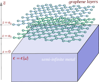
In our formalism, we consider a nano-scale system consisting of a pair of 2D layers and a thick conducting material. The layer may be monolayer graphene or a 2DEG such as a semiconductor inversion layer or HEMT (high electron mobility transistor). The graphene layer may have a gap, thereby extending the flexibility of the composite system that also incorporates a thick layer of conducting material as depicted in Fig. 1. The excitation spectra of allowable modes will be determined from a knowledge of the non-local dielectric function ϵ(𝐫,𝐫;ω)italic-ϵ𝐫superscript𝐫𝜔\epsilon({\bf r},{\bf r}^{\prime};\omega) which depends on position coordinates 𝐫,𝐫𝐫superscript𝐫{\bf r},{\bf r}^{\prime} and frequency ω𝜔\omega or its inverse K(𝐫,𝐫;ω)𝐾𝐫superscript𝐫𝜔K({\bf r},{\bf r}^{\prime};\omega) satisfying 𝑑𝐫K(𝐫,𝐫;ω)ϵ(𝐫,𝐫′′;ω)=δ(𝐫𝐫′′)differential-dsuperscript𝐫𝐾𝐫superscript𝐫𝜔italic-ϵsuperscript𝐫superscript𝐫′′𝜔𝛿𝐫superscript𝐫′′\int d{\bf r}^{\prime}\ K({\bf r},{\bf r}^{\prime};\omega)\,\epsilon({\bf r}^{\prime},{\bf r}^{\prime\prime};\omega)=\delta({\bf r}-{\bf r}^{\prime\prime}). The self-consistent field equation for K(𝐫,𝐫;ω)𝐾𝐫superscript𝐫𝜔K({\bf r},{\bf r}^{\prime};\omega) is now determined.

Refer to caption
Figure 1: (Color online) Schematic illustration of a spiler generator consisting of a thick (semi- infinite) conducting material on whose surface a plasmon resonance may induce an instability by coupling to the 2D plasmons on a pair of thin layers such as graphene, silicene or 2DEG at a hetero-interface.

In operator notation, the dielectric function for the 2D layer and semi-infinite structure is given by

ϵ^=1^+α^SI+α^2Dϵ^SI+α^2D=K^SI1+α^2D,^italic-ϵ^1subscript^𝛼𝑆𝐼subscript^𝛼2𝐷subscript^italic-ϵ𝑆𝐼subscript^𝛼2𝐷superscriptsubscript^𝐾𝑆𝐼1subscript^𝛼2𝐷\hat{\epsilon}=\hat{1}+\hat{\alpha}_{SI}+\hat{\alpha}_{2D}\equiv\hat{\epsilon}_{SI}+\hat{\alpha}_{2D}=\hat{K}_{SI}^{-1}+\hat{\alpha}_{2D}\ , (1)

where ϵ^=K^1^italic-ϵsuperscript^𝐾1\hat{\epsilon}=\hat{K}^{-1} with K^^𝐾\hat{K} as the inverse dielectric function satisfying

K^=K^SIK^SIα^2DK^.^𝐾subscript^𝐾𝑆𝐼subscript^𝐾𝑆𝐼subscript^𝛼2𝐷^𝐾\hat{K}=\hat{K}_{SI}-\hat{K}_{SI}\cdot\hat{\alpha}_{2D}\cdot\hat{K}\ . (2)

Here, α^^𝛼\hat{\alpha}, α^2Dsubscript^𝛼2𝐷\hat{\alpha}_{2D} and α^SIsubscript^𝛼𝑆𝐼\hat{\alpha}_{SI} are the polarization functions of the composite system, the polarization function of the 2D layer and semi-infinite substrate, respectively. Additionally, K^SIsubscript^𝐾𝑆𝐼\hat{K}_{SI} is the inverse dielectric function for the semi-infinite substrate whose surface lies in the z=0𝑧0z=0 plane. In integral form, after Fourier transforming with respect to coordinates parallel to the xy𝑥𝑦xy-plane and suppressing the in-plane wave number q||q_{||} and frequency ω𝜔\omega, we obtain

K(z1,z2)=KSI(z1,z2)𝑑z𝑑z′′K(z1,z)α2D(z,z′′)K(z′′,z2).𝐾subscript𝑧1subscript𝑧2subscript𝐾𝑆𝐼subscript𝑧1subscript𝑧2superscriptsubscriptdifferential-dsuperscript𝑧superscriptsubscriptdifferential-dsuperscript𝑧′′𝐾subscript𝑧1superscript𝑧subscript𝛼2𝐷superscript𝑧superscript𝑧′′𝐾superscript𝑧′′subscript𝑧2K(z_{1},z_{2})=K_{SI}(z_{1},z_{2})-\int_{-\infty}^{\infty}dz^{\prime}\int_{-\infty}^{\infty}dz^{\prime\prime}\ K(z_{1},z^{\prime})\,\alpha_{2D}(z^{\prime},z^{\prime\prime})\,K(z^{\prime\prime},z_{2})\ . (3)

Here, the polarization function for the 2D structure is given by

α2D(z,z′′)=𝑑z′′′v(zz′′′)D(z′′′,z′′),subscript𝛼2𝐷superscript𝑧superscript𝑧′′superscriptsubscriptdifferential-dsuperscript𝑧′′′𝑣superscript𝑧superscript𝑧′′′𝐷superscript𝑧′′′superscript𝑧′′\alpha_{2D}(z^{\prime},z^{\prime\prime})=\int_{-\infty}^{\infty}dz^{\prime\prime\prime}\ v(z^{\prime}-z^{\prime\prime\prime})\,D(z^{\prime\prime\prime},z^{\prime\prime})\ , (4)

where v(zz)=(2πe2/ϵsq)exp(q|zz|)𝑣𝑧superscript𝑧2𝜋superscript𝑒2subscriptitalic-ϵ𝑠subscript𝑞parallel-tosubscript𝑞parallel-to𝑧superscript𝑧v(z-z^{\prime})=(2\pi e^{2}/\epsilon_{s}q_{\parallel})\,\exp(-q_{\parallel}|z-z^{\prime}|), ϵs=4πϵ0ϵrsubscriptitalic-ϵ𝑠4𝜋subscriptitalic-ϵ0subscriptitalic-ϵ𝑟\epsilon_{s}=4\pi\epsilon_{0}\epsilon_{r}, and the 2D response function obeys

D(z′′′,z′′)=Π2D(0)(q||,ω)δ(z′′′a)δ(z′′a)D(z^{\prime\prime\prime},z^{\prime\prime})=\Pi_{2D}^{(0)}(q_{||},\omega)\,\delta(z^{\prime\prime\prime}-a)\,\delta(z^{\prime\prime}-a) (5)

with Π2D(0)(q||,ω)\Pi_{2D}^{(0)}(q_{||},\omega) as the single-particle in-plane response. Upon substituting this form of the polarization function for the monolayer into the integral equation for the inverse dielectric function, we have

K(z1,z2)=KSI(z1,z2)Π2D(0)(q||,ω)𝑑zKSI(z1,z)v(za)K(a,z2).K(z_{1},z_{2})=K_{SI}(z_{1},z_{2})-\Pi_{2D}^{(0)}(q_{||},\omega)\int_{-\infty}^{\infty}dz^{\prime}\ K_{SI}(z_{1},z^{\prime})\,v(z^{\prime}-a)\,K(a,z_{2})\ . (6)

We now set z1=asubscript𝑧1𝑎z_{1}=a in Eq. (6) and obtain

K(a,z2)=KSI(a,z2)Π2D(0)(q||,ω){𝑑zKSI(a,z)v(za)}K(a,z2).K(a,z_{2})=K_{SI}(a,z_{2})-\Pi_{2D}^{(0)}(q_{||},\omega)\left\{\int_{-\infty}^{\infty}dz^{\prime}\ K_{SI}(a,z^{\prime})\,v(z^{\prime}-a)\right\}K(a,z_{2})\ . (7)

Solving for K(a,z2)𝐾𝑎subscript𝑧2K(a,z_{2}) yields

K(a,z2)=KSI(a,z2)SC(q||,ω),K(a,z_{2})=\frac{K_{SI}(a,z_{2})}{S_{C}(q_{||},\omega)}\ , (8)

and

SC(q||,ω)1+Π2D(0)(q||,ω){𝑑zKSI(a,z)v(za)}S_{C}(q_{||},\omega)\equiv 1+\Pi_{2D}^{(0)}(q_{||},\omega)\left\{\int_{-\infty}^{\infty}dz^{\prime}\ K_{SI}(a,z^{\prime})\,v(z^{\prime}-a)\right\} (9)

whose zeros determine the plasmon resonances. In our numerical calculations, we shall use KSI(z,z)subscript𝐾𝑆𝐼𝑧superscript𝑧K_{SI}(z,z^{\prime}) given in Eq. (30) of Ref. [Horing, ]. Thus, from Eq. (6), we obtain

K(z1,z2)=KSI(z1,z2)Π2D(0)(q||,ω)KSI(a,z2)SC(q||,ω){𝑑zKSI(z1,z)v(za)}.K(z_{1},z_{2})=K_{SI}(z_{1},z_{2})-\Pi_{2D}^{(0)}(q_{||},\omega)\frac{K_{SI}(a,z_{2})}{S_{C}(q_{||},\omega)}\left\{\int_{-\infty}^{\infty}\ dz^{\prime}\ K_{SI}(z_{1},z^{\prime})v(z^{\prime}-a)\right\}\ \ . (10)

In the local limit, we have

SC(q||,ω)=1+2πe2ϵsq||Π2D(0)(q||,ω){1+e2q||a1ϵB(ω)1+ϵB(ω)}.S_{C}(q_{||},\omega)=1+\frac{2\pi e^{2}}{\epsilon_{s}q_{||}}\,\Pi_{2D}^{(0)}(q_{||},\omega)\left\{1+e^{-2q_{||}a}\frac{1-\epsilon_{B}(\omega)}{1+\epsilon_{B}(\omega)}\right\}\ . (11)

With Π2D(0)(q||,ω)Cq2/ω2\Pi_{2D}^{(0)}(q_{||},\omega)\approx Cq_{\parallel}^{2}/\omega^{2}, we obtain the following equation:

12πCe2ϵsω2q{1+e2qaωp22ω2ωp2}=0,12𝜋𝐶superscript𝑒2subscriptitalic-ϵ𝑠superscript𝜔2subscript𝑞parallel-to1superscript𝑒2subscript𝑞parallel-to𝑎superscriptsubscript𝜔𝑝22superscript𝜔2superscriptsubscript𝜔𝑝201-\frac{2\pi Ce^{2}}{\epsilon_{s}\omega^{2}}q_{\parallel}\left\{1+e^{-2q_{\parallel}a}\,\frac{\omega_{p}^{2}}{2\omega^{2}-\omega_{p}^{2}}\right\}=0\,, (12)

which is a quadratic equation for ω2superscript𝜔2\omega^{2}. For a 2DEG, we have C=n2D/m2D𝐶subscript𝑛2𝐷superscriptsubscript𝑚2𝐷C=n_{2D}/m_{2D}^{\ast}. For graphene,

C=2μπ2{1Δ2μ2},𝐶2𝜇𝜋superscriptPlanck-constant-over-2-pi21superscriptΔ2superscript𝜇2C=\frac{2\mu}{\pi\hbar^{2}}\left\{1-\frac{\Delta^{2}}{\mu^{2}}\right\}\ , (13)

where μ𝜇\mu is the chemical potential and ΔΔ\Delta is the gap between valence and conduction bands. Consequently, we find the plasmon frequency as follows: NJMH

ω2=K1±K2superscript𝜔2plus-or-minussubscript𝐾1subscript𝐾2\omega^{2}=K_{1}\pm\sqrt{K_{2}} (14)

with K1subscript𝐾1K_{1} and K2subscript𝐾2K_{2} defined by:

K1=πe2Cϵsq+(ωp2)2,subscript𝐾1𝜋superscript𝑒2𝐶subscriptitalic-ϵ𝑠subscript𝑞parallel-tosuperscriptsubscript𝜔𝑝22\displaystyle K_{1}=\frac{\pi e^{2}C}{\epsilon_{s}}q_{\parallel}+\left(\frac{\omega_{p}}{2}\right)^{2}\ ,
K2=πe2Cωp2ϵse2qaq+[(ωp2)2Ce2πϵsq]2.subscript𝐾2𝜋superscript𝑒2𝐶superscriptsubscript𝜔𝑝2subscriptitalic-ϵ𝑠superscript𝑒2subscript𝑞parallel-to𝑎subscript𝑞parallel-tosuperscriptdelimited-[]superscriptsubscript𝜔𝑝22𝐶superscript𝑒2𝜋subscriptitalic-ϵ𝑠subscript𝑞parallel-to2\displaystyle K_{2}=\frac{\pi e^{2}C\,\omega_{p}^{2}}{\epsilon_{s}}e^{-2q_{\parallel}a}\,q_{\parallel}+\left[\left(\frac{\omega_{p}}{2}\right)^{2}-\frac{Ce^{2}\pi}{\epsilon_{s}}q_{\parallel}\right]^{2}\,. (15)

In the long-wavelength limit (qkF)much-less-thansubscript𝑞parallel-tosubscript𝑘𝐹(q_{\parallel}\ll k_{F}) these expressions are reduced to:

ω124πCe2aϵsq2,superscriptsubscript𝜔124𝜋𝐶superscript𝑒2𝑎subscriptitalic-ϵ𝑠superscriptsubscript𝑞parallel-to2\displaystyle\omega_{1}^{2}\approx\frac{4\pi Ce^{2}a}{\epsilon_{s}}q_{\parallel}^{2}\ , (16)
ω22ωp22+2πCe2ϵsq,superscriptsubscript𝜔22superscriptsubscript𝜔𝑝222𝜋𝐶superscript𝑒2subscriptitalic-ϵ𝑠subscript𝑞parallel-to\displaystyle\omega_{2}^{2}\approx\frac{\omega_{p}^{2}}{2}+\frac{2\pi Ce^{2}}{\epsilon_{s}}q_{\parallel}\ ,

and the frequencies are

ω12eπaCϵsq,subscript𝜔12𝑒𝜋𝑎𝐶subscriptitalic-ϵ𝑠subscript𝑞parallel-to\displaystyle\omega_{1}\approx 2e\sqrt{\frac{\pi aC}{\epsilon_{s}}}\,q_{\parallel}\ , (17)
ω2ωp2+2πCe2ϵsωpq,subscript𝜔2subscript𝜔𝑝22𝜋𝐶superscript𝑒2subscriptitalic-ϵ𝑠subscript𝜔𝑝subscript𝑞parallel-to\displaystyle\omega_{2}\approx\frac{\omega_{p}}{\sqrt{2}}+\frac{\sqrt{2}\pi Ce^{2}}{\epsilon_{s}\omega_{p}}\,q_{\parallel}\ ,

which are both linear in q||q_{||}, unlike the q||1/2q_{||}^{1/2}-dependence for free-standing graphene or the 2DEG 7 ; 8 ; 9 ; 10 ; wunch ; pavlo .

We may generalize the formalism to a structure with a double layer positioned at z=a1𝑧subscript𝑎1z=a_{1} and z=a2𝑧subscript𝑎2z=a_{2} (0<a1<a20subscript𝑎1subscript𝑎20<a_{1}<a_{2}) interacting with each other as well as the semi-infinite conducting substrate with its surface located at z=0𝑧0z=0. A similar calculation shows that

K(z1,z2)𝐾subscript𝑧1subscript𝑧2\displaystyle K(z_{1},z_{2}) =\displaystyle= KSI(z1,z2)Π2D;1(0)(q||,ω)𝑑zKSI(z1,z)v(za1)K(a1,z2)\displaystyle K_{SI}(z_{1},z_{2})-\Pi_{2D;1}^{(0)}(q_{||},\omega)\int_{-\infty}^{\infty}dz^{\prime}\ K_{SI}(z_{1},z^{\prime})v(z^{\prime}-a_{1})K(a_{1},z_{2}) (18)
\displaystyle- Π2D;2(0)(q||,ω)𝑑zKSI(z1,z)v(za2)K(a2,z2).\displaystyle\Pi_{2D;2}^{(0)}(q_{||},\omega)\int_{-\infty}^{\infty}dz^{\prime}\ K_{SI}(z_{1},z^{\prime})v(z^{\prime}-a_{2})K(a_{2},z_{2})\ .

By setting z1=a1subscript𝑧1subscript𝑎1z_{1}=a_{1} and z1=a2subscript𝑧1subscript𝑎2z_{1}=a_{2} in turn in Eq. (18) and solving the pair of simultaneous equations for K(a1,z2)𝐾subscript𝑎1subscript𝑧2K(a_{1},z_{2}) and K(a2,z2)𝐾subscript𝑎2subscript𝑧2K(a_{2},z_{2}), we obtain

[K(a1,z2)K(a2,z2)]=1Sc(2)(q||,ω)(q||,ω)[KSI(a1,z2)KSI(a2,z2)],\left[\begin{matrix}K(a_{1},z_{2})\cr K(a_{2},z_{2})\cr\end{matrix}\right]=\frac{1}{S_{c}^{(2)}(q_{||},\omega)}\tensor{{\cal M}}(q_{||},\omega)\left[\begin{matrix}K_{SI}(a_{1},z_{2})\cr K_{SI}(a_{2},z_{2})\cr\end{matrix}\right]\ , (19)

where Sc(2)(q||,ω)=Det(q||,ω)S_{c}^{(2)}(q_{||},\omega)=\mbox{Det}\tensor{{\cal M}}(q_{||},\omega) with

(q||,ω)=\tensor{{\cal M}}(q_{||},\omega)=
[1+Π2D;2(0)(q||,ω)𝑑zKSI(a2,z)v(za2)Π2D;2(0)(q||,ω)𝑑zKSI(a1,z)v(za2)Π2D;1(0)(q||,ω)𝑑zKSI(a2,z)v(za1)1+Π2D;1(0)(q||,ω)𝑑zKSI(a1,z)v(za1)].\left[\begin{array}[]{cc}1+\Pi_{2D;2}^{(0)}(q_{||},\omega)\int\limits_{-\infty}^{\infty}dz^{\prime}K_{SI}(a_{2},z^{\prime})v(z^{\prime}-a_{2})&-\Pi_{2D;2}^{(0)}(q_{||},\omega)\int\limits_{-\infty}^{\infty}dz^{\prime}K_{SI}(a_{1},z^{\prime})v(z^{\prime}-a_{2})\cr-\Pi_{2D;1}^{(0)}(q_{||},\omega)\int\limits_{-\infty}^{\infty}dz^{\prime}K_{SI}(a_{2},z^{\prime})v(z^{\prime}-a_{1})&1+\Pi_{2D;1}^{(0)}(q_{||},\omega)\int\limits_{-\infty}^{\infty}dz^{\prime}K_{SI}(a_{1},z^{\prime})v(z^{\prime}-a_{1})\end{array}\right]\ . (20)

Substituting the results for K(a1,z2)𝐾subscript𝑎1subscript𝑧2K(a_{1},z_{2}) and K(a2,z2)𝐾subscript𝑎2subscript𝑧2K(a_{2},z_{2}) into Eq. (18), we obtain the complete inverse dielectric function for a pair of 2D planes interacting with each other and a semi-infinite conducting material. The plasmon excitation frequencies are determined by the zeros of Sc(2)(q||,ω)S_{c}^{(2)}(q_{||},\omega). Furthermore, the effect of the inverse dielectric function for the semi-infinite structure KSI(z,z;q||,ω)K_{SI}(z,z^{\prime};q_{||},\omega) screens coupling within and between two layers. As a matter of fact, our result for the plasmon dispersion relation generalizes that obtained by Das Sarma and Madhukar DasSarma for a bi-plane. In the current case, we obtain in the local limit

Sc(2)(q||,ω)={1+2πe2ϵsq||Π2D;2(0)(q||,ω)[1+e2q||a2ωp22ω2ωp2]}\displaystyle S_{c}^{(2)}(q_{||},\omega)=\left\{1+\frac{2\pi e^{2}}{\epsilon_{s}q_{||}}\,\Pi_{2D;2}^{(0)}(q_{||},\omega)\left[1+e^{-2q_{||}a_{2}}\,\frac{\omega_{p}^{2}}{2\omega^{2}-\omega_{p}^{2}}\right]\right\} (21)
×\displaystyle\times {1+2πe2ϵsq||Π2D;1(0)(q||,ω)[1+e2q||a1ωp22ω2ωp2]}\displaystyle\left\{1+\frac{2\pi e^{2}}{\epsilon_{s}q_{||}}\,\Pi_{2D;1}^{(0)}(q_{||},\omega)\left[1+e^{-2q_{||}a_{1}}\,\frac{\omega_{p}^{2}}{2\omega^{2}-\omega_{p}^{2}}\right]\right\}
\displaystyle- (2πe2ϵsq||)2Π2D;1(0)(q||,ω)Π2D;2(0)(q||,ω)[eq|||a1a2|+eq||(a1+a2)ωp22ω2ωp2]2.\displaystyle\left(\frac{2\pi e^{2}}{\epsilon_{s}q_{||}}\right)^{2}\Pi_{2D;1}^{(0)}(q_{||},\omega)\,\Pi_{2D;2}^{(0)}(q_{||},\omega)\left[e^{-q_{||}|a_{1}-a_{2}|}+e^{-q_{||}(a_{1}+a_{2})}\,\frac{\omega_{p}^{2}}{2\omega^{2}-\omega_{p}^{2}}\right]^{2}\ .

We now introduce our notation, C¯j=2πe2Cj/(ϵsωp2)subscript¯𝐶𝑗2𝜋superscript𝑒2subscript𝐶𝑗subscriptitalic-ϵ𝑠superscriptsubscript𝜔𝑝2\overline{C}_{j}=2\pi e^{2}C_{j}/(\epsilon_{s}\omega_{p}^{2}) for j=1,2𝑗12j=1,2. The spectral function yields real frequencies. A plane interacting with the half-space has two resonant modes. Each pair of 2D layers interacting in isolation far from the half-space conducting medium supports a symmetric and an antisymmetric mode DasSarma . In the absence of a driving current, the analytic solutions for the plasmon modes for a pair of 2D layers that are Coulomb coupled to a half-space are given by

Ω1(q)/ωp=1/2+q(C¯1+C¯2)/2+𝒪[q2],subscriptΩ1subscript𝑞parallel-tosubscript𝜔𝑝12subscript𝑞parallel-tosubscript¯𝐶1subscript¯𝐶22𝒪delimited-[]superscriptsubscript𝑞parallel-to2\displaystyle\Omega_{1}(q_{\parallel})/\omega_{p}=1/\sqrt{2}+q_{\parallel}\,(\overline{C}_{1}+\overline{C}_{2})/\sqrt{2}+\mathcal{O}[q_{\parallel}^{2}]\ , (22)
Ω2(q)/ωp=qC¯1a1+C¯2a2+𝒜+𝒪[q2],subscriptΩ2subscript𝑞parallel-tosubscript𝜔𝑝subscript𝑞parallel-tosubscript¯𝐶1subscript𝑎1subscript¯𝐶2subscript𝑎2𝒜𝒪delimited-[]superscriptsubscript𝑞parallel-to2\displaystyle\Omega_{2}(q_{\parallel})/\omega_{p}=q_{\parallel}\sqrt{\overline{C}_{1}a_{1}+\overline{C}_{2}a_{2}+\sqrt{\mathcal{A}}}+\mathcal{O}[q_{\parallel}^{2}]\ ,
Ω3(q)/ωp=qC¯1a1+C¯2a2𝒜+𝒪[q2],subscriptΩ3subscript𝑞parallel-tosubscript𝜔𝑝subscript𝑞parallel-tosubscript¯𝐶1subscript𝑎1subscript¯𝐶2subscript𝑎2𝒜𝒪delimited-[]superscriptsubscript𝑞parallel-to2\displaystyle\Omega_{3}(q_{\parallel})/\omega_{p}=q_{\parallel}\sqrt{\overline{C}_{1}a_{1}+\overline{C}_{2}a_{2}-\sqrt{\mathcal{A}}}+\mathcal{O}[q_{\parallel}^{2}]\ ,

where 𝒜(C¯1a1C¯2a2)2+4C¯1C¯2a12𝒜superscriptsubscript¯𝐶1subscript𝑎1subscript¯𝐶2subscript𝑎224subscript¯𝐶1subscript¯𝐶2superscriptsubscript𝑎12\mathcal{A}\equiv(\overline{C}_{1}a_{1}-\overline{C}_{2}a_{2})^{2}+4\overline{C}_{1}\overline{C}_{2}a_{1}^{2} and the term 4C¯1C¯2a124subscript¯𝐶1subscript¯𝐶2superscriptsubscript𝑎124\overline{C}_{1}\overline{C}_{2}a_{1}^{2} plays the role of “Rabi coupling”. Clearly, for long wavelengths, only Ω1(q)subscriptΩ1subscript𝑞parallel-to\Omega_{1}(q_{\parallel}) depends on ωpsubscript𝜔𝑝\omega_{p}. However, the excitation spectrum changes dramatically when a current is driven through the configuration. Under a constant electric field, the carrier distribution is modified, as may be obtained by employing the relaxation time approximation in the equation of motion for the center-of-mass momentum. For carriers in a parabolic energy band with effective mass msuperscript𝑚m^{\ast} and drift velocity 𝐯dsubscript𝐯𝑑{\bf v}_{d} determined by the electron mobility and the external electric field, the electrons in the medium are redistributed. This is determined by a momentum shift in the wave vector 𝐤𝐤m𝐯d/subscript𝐤parallel-tosubscript𝐤parallel-tosuperscript𝑚subscript𝐯𝑑Planck-constant-over-2-pi{\bf k}_{\parallel}\to{\bf k}_{\parallel}-m^{\ast}{\bf v}_{d}/\hbar in the thermal-equilibrium energy distribution function f0(ϵ𝐤)subscript𝑓0subscriptitalic-ϵ𝐤f_{0}(\epsilon_{\bf k}). By making a change of variables in the well-known Lindhard polarization function Π2D(0)(q,ω)subscriptsuperscriptΠ02𝐷subscript𝑞parallel-to𝜔\Pi^{(0)}_{2D}(q_{\parallel},\omega), this effect is equivalent to a frequency shift ωω𝐪𝐯d𝜔𝜔subscript𝐪parallel-tosubscript𝐯𝑑\omega\to\omega-{\bf q}_{\parallel}\cdot{\bf v}_{d}. For massless Dirac fermions in graphene with linear energy dispersion, this Doppler shift in frequency is not in general valid for arbitrary wave vector as we prove in our Appendix. This is our conclusion after we relate the surface current density to the center-of-mass wave vector in a steady state. Our calculation shows that the redistribution of electrons leads to a shift in the wave vector appearing in the Fermi function by the center-of-mass wave vector 𝐊0=(kF/vF)𝐯dsubscript𝐊0subscript𝑘𝐹subscript𝑣𝐹subscript𝐯𝑑{\bf K}_{0}=(k_{F}/v_{F}){\bf v}_{d} where kFsubscript𝑘𝐹k_{F} and vFsubscript𝑣𝐹v_{F} are the Fermi wave vector and velocity, respectively. However, in the long wavelength limit, q0subscript𝑞parallel-to0q_{\parallel}\to 0, the Doppler shift in frequency is approximately obeyed. This is discussed in Appendix A. Consequently, regardless of the nature of the 2D layer represented in the dispersion equation we may replace ωω𝐪𝐯d𝜔𝜔subscript𝐪parallel-tosubscript𝐯𝑑\omega\to\omega-{\bf q}_{\parallel}\cdot{\bf v}_{d} in the dispersion equation in the presence of an applied electric field at long wavelengths.

We shall treat the solution frequencies ω±(q)subscript𝜔plus-or-minussubscript𝑞parallel-to\omega_{\pm}(q_{\parallel}) as complex variables with Im[ω±(q)]0Imdelimited-[]subscript𝜔plus-or-minussubscript𝑞parallel-to0{\rm Im}[\omega_{\pm}(q_{\parallel})]\geq 0, where Im[ω±(q)]>0Imdelimited-[]subscript𝜔plus-or-minussubscript𝑞parallel-to0{\rm Im}[\omega_{\pm}(q_{\parallel})]>0 implies a finite growth rates γ±(q)=Im[ω±(q)]subscript𝛾plus-or-minussubscript𝑞parallel-toImdelimited-[]subscript𝜔plus-or-minussubscript𝑞parallel-to\gamma_{\pm}(q_{\parallel})={\rm Im}[\omega_{\pm}(q_{\parallel})] for two split plasmon modes. Since ϵ(q,ω)italic-ϵsubscript𝑞parallel-to𝜔\epsilon(q_{\parallel},\,\omega) is a complex function, we ask for Re[ϵ(q,ω)]=Im[ϵ(q,ω)]=0Redelimited-[]italic-ϵsubscript𝑞parallel-to𝜔Imdelimited-[]italic-ϵsubscript𝑞parallel-to𝜔0{\rm Re}[\epsilon(q_{\parallel},\,\omega)]={\rm Im}[\epsilon(q_{\parallel},\,\omega)]=0. Therefore, we are left with damping-free plasmon modes in the system but they still face possible instability due to Im[ω±(q)]>0Imdelimited-[]subscript𝜔plus-or-minussubscript𝑞parallel-to0{\rm Im}[\omega_{\pm}(q_{\parallel})]>0.

III Numerical Results and Discussion

First, we have investigated numerically the effect of passing a current through a layer of 2DEG, graphene or silicene in the presence of a surface, for a pair of 2D layers and a semi-infinite conducting medium as presented in Fig. 1. In Fig. 2, we present the complex frequencies which yield the plasmon dispersion (real part) and inverse lifetime (imaginary part). The layers are located at z=a1=0.1C¯1𝑧subscript𝑎10.1subscript¯𝐶1z=a_{1}=0.1\,\bar{C}_{1} and z=a2=0.4C¯1𝑧subscript𝑎20.4subscript¯𝐶1z=a_{2}=0.4\,\bar{C}_{1}. Each panel presents results for a different drift velocity vd/ωp=0subscript𝑣𝑑subscript𝜔𝑝0v_{d}/\omega_{p}=0, 0.5C¯10.5subscript¯𝐶10.5\,\bar{C}_{1}, 0.8C¯10.8subscript¯𝐶10.8\,\bar{C}_{1} and 1.6C¯11.6subscript¯𝐶11.6\,\bar{C}_{1}. In the absence of a drift current, (vd=0subscript𝑣𝑑0v_{d}=0), panel (a)𝑎(a) shows that there are three plasmon branches excited, which are stable as given by Eq. (II). At low drift velocity, panel (b)𝑏(b) shows that the plasmons are still stable. However, as the current is increased, the lowest branches may become unstable as demonstrated in panels (c)𝑐(c) and (d)𝑑(d) through the appearance of a finite imaginary part for the frequency. The carrier concentrations, chemical potentials or temperatures in the layers are such that C¯1=1.2C¯2subscript¯𝐶11.2subscript¯𝐶2\bar{C}_{1}=1.2\,\bar{C}_{2} for all cases. Either of the two lowest plasmon branches might become unstable, depending on the strength of the drift current. The Rabi splitting of the plasmon branches in the presence of an external electric field is a consequence of quasiparticles having different energies for the same wavelength.

Refer to caption
Figure 2: (Color online) Complex frequencies ω𝜔\omega yielding the plasmon dispersion (real part [ω]delimited-[]𝜔\mathfrak{R}[\omega]) and inverse lifetime (imaginary part [ω]delimited-[]𝜔\mathfrak{I}[\omega]) for a pair of 2D layers and a semi-infinite conducting medium as presented in Fig. 1. The plasma frequency for the semi-infinite medium is ωpsubscript𝜔𝑝\omega_{p}. The layers are located at a1=0.1C¯1subscript𝑎10.1subscript¯𝐶1a_{1}=0.1\,\bar{C}_{1} and a2=0.4C¯1subscript𝑎20.4subscript¯𝐶1a_{2}=0.4\,\bar{C}_{1} with respect to the surface. Each panel corresponds to a different drift velocity vd/ωp=0subscript𝑣𝑑subscript𝜔𝑝0v_{d}/\omega_{p}=0, 0.5C¯10.5subscript¯𝐶10.5\,\bar{C}_{1}, 0.8C¯10.8subscript¯𝐶10.8\,\bar{C}_{1} and 1.6C¯11.6subscript¯𝐶11.6\,\bar{C}_{1}. Panel (a)𝑎(a) with vd=0subscript𝑣𝑑0v_{d}=0 corresponds to the solutions in Eq. (II). Panel (b)𝑏(b) shows that for a small drift vdsubscript𝑣𝑑v_{d} additional plasmon branch appears, but all solutions are stable. The carrier concentrations, chemical potentials or temperatures in the layers are such that C¯1=1.2C¯2subscript¯𝐶11.2subscript¯𝐶2\bar{C}_{1}=1.2\,\bar{C}_{2} for all cases. Either of the two lowest plasmon branches might become unstable, depending on vdsubscript𝑣𝑑v_{d}. The Rabi splitting of the plasmon excitation branches by the external electric field is attributed to quasiparticles with different excitation energies for the same wavelength. After the “loop” closes in (c)𝑐(c), the lowest branch becomes unstable with finite imaginary part illustrated by the red curve. In (d)𝑑(d), the lowest plasmon branch has an instability for two separate ranges of wave vector.

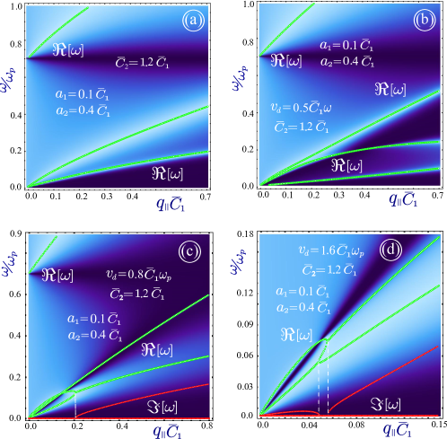
From the perspective of real space, the plasmon wave is a longitudinal charge density wave with both its density fluctuation and phase velocity vpsubscript𝑣𝑝v_{p} along the 𝐪subscript𝐪parallel-to{\bf q}_{\parallel} (propagation) direction. When there are two electron gas layers separated by a distance ΔaΔ𝑎\Delta a in the z𝑧z direction, the inter-layer coulomb coupling will produce two plasmon modes with different energy dispersions ω±(q)subscript𝜔plus-or-minussubscript𝑞parallel-to\omega_{\pm}(q_{\parallel}) and phase velocities v±(q)=ω±(q)/qsubscript𝑣plus-or-minussubscript𝑞parallel-tosubscript𝜔plus-or-minussubscript𝑞parallel-tosubscript𝑞parallel-tov_{\pm}(q_{\parallel})=\omega_{\pm}(q_{\parallel})/q_{\parallel}, which are separately associated with the symmetric [in-phase, upper ω+(q)subscript𝜔subscript𝑞parallel-to\omega_{+}(q_{\parallel}) branch in Fig. 2(a)] and antisymmetric [out-of-phase, lower ω(q)subscript𝜔subscript𝑞parallel-to\omega_{-}(q_{\parallel}) branch] states of charge-density waves. The symmetric plasmon mode gives rise to a dipole-like plasmon excitation, similar in nature to that of a single layer with an electron density given by adding the densities on the two layers. On the other hand, the antisymmetric plasmon mode leads to a quadruple-like excitation, which is able to store electric field energy between the two layers. In the presence of a current with drift velocity vdsubscript𝑣𝑑v_{d} for electrons in one of the two electron-gas layers, the phase velocities of these two spatially separated plasmon modes are modified drastically due to the Doppler shift as well as the surface plasmon on the substrate. Consequently, two streams of quasiparticles with different phase velocities may be created from either the symmetric or antisymmetric mode, depending on the strength of the current, the separation between layers and their distances from the surface of the substrate. However, for freely suspended layers, the lower-energy antisymmetric plasmon mode becomes unstable whenever vdsubscript𝑣𝑑v_{d} lies within the range v(q)<vd<v+(q)subscript𝑣subscript𝑞parallel-tosubscript𝑣𝑑subscript𝑣subscript𝑞parallel-tov_{-}(q_{\parallel})<v_{d}<v_{+}(q_{\parallel}), switching from a quadruple-like excitation to a dipole-like excitation. The instability for the plasmon mode has a finite lifetime because it grows after taking energy from the injected current and transferring it to the incident electromagnetic field.

From the point of view of momentum space, electrons may only occupy momentum space within the range of |𝐤|kFsubscript𝐤parallel-tosubscript𝑘𝐹|{\bf k}_{\parallel}|\leq k_{F} at zero temperature in a state of thermal equilibrium, where kFsubscript𝑘𝐹k_{F} is the electron Fermi wave number and ε(kF)=ε(kF)=EF𝜀subscript𝑘𝐹𝜀subscript𝑘𝐹subscript𝐸𝐹\varepsilon(k_{F})=\varepsilon(-k_{F})=E_{F} is the Fermi energy. When a current is passed through the electron gas, electrons are driven out from this state of thermal equilibrium and their population becomes asymmetrical with respect to k=0subscript𝑘parallel-to0k_{\parallel}=0. In this case, the Fermi energy EFsubscript𝐸𝐹E_{F} is split into EF,+=ε(kF+Kc)subscript𝐸𝐹𝜀subscript𝑘𝐹subscript𝐾𝑐E_{F,+}=\varepsilon(k_{F}+K_{c}) and EF,=ε(kF+Kc)subscript𝐸𝐹𝜀subscript𝑘𝐹subscript𝐾𝑐E_{F,-}=\varepsilon(-k_{F}+K_{c}) with EF,+>EF,subscript𝐸𝐹subscript𝐸𝐹E_{F,+}>E_{F,-}, where KcPlanck-constant-over-2-pisubscript𝐾𝑐\hbar K_{c} represents the electron center-of-mass momentum. In this shifted Fermi-Dirac distribution model, electrons in such a non-equilibrium state are energetically unstable, and the higher-energy electrons in the range kFkkF+Kcsubscript𝑘𝐹subscript𝑘parallel-tosubscript𝑘𝐹subscript𝐾𝑐k_{F}\leq k_{\parallel}\leq k_{F}+K_{c} tend to relax to the lower-energy empty states in the range of kFkKckFsubscript𝑘𝐹subscript𝑘parallel-tosubscript𝐾𝑐subscript𝑘𝐹-k_{F}\leq k_{\parallel}\leq K_{c}-k_{F} by emitting electromagnetic waves and phonons to ensure total momentum and energy conservation. This process is known as radiation loss of plasmon excitations in the time domain, in addition to the usual absorption loss of plasmon excitations in the space domain due to nonzero imaginary part of the electron dielectric function.

A surface grating must be employed in order to convert the energy of the unstable plasmon mode into a transverse radiation field in free space and at the same time suppress phonon emission (heating). The growth rate γp(q)=Im[ωp(q)]subscript𝛾𝑝subscript𝑞parallel-toImdelimited-[]subscript𝜔𝑝subscript𝑞parallel-to\gamma_{p}(q_{\parallel})={\rm Im}[\omega_{p}(q_{\parallel})] of the plasmon mode is determined by the imaginary part of the plasmon frequency while the average plasmon growth rate (per unit area) is given by γ(Kc)=(2π)10𝑑qγp(q)q𝛾subscript𝐾𝑐superscript2𝜋1superscriptsubscript0differential-dsubscript𝑞parallel-tosubscript𝛾𝑝subscript𝑞parallel-tosubscript𝑞parallel-to\gamma(K_{c})=(2\pi)^{-1}\int\limits_{0}^{\infty}\,dq_{\parallel}\ \gamma_{p}(q_{\parallel})\,q_{\parallel}.

IV Concluding Remarks

In summary, we are proposing a spiler quantum plasmonic device which employs 2D layers in combination with a thick conducting material. We find that the spiler emits electromagnetic radiation when a current is passed through the 2D layer or the surface of the thick conducting material to make the plasmons become unstable at a specific frequency and wave number. It is possible to change the range of plasmon instability by selecting the properties of the nanosheet or frequency of the surface plasmon, i.e., the substrate. The surface plasmon plays a crucial role in giving rise to the Rabi splitting and the concomitant streams of quasiparticles whose phase velocities are in opposite directions when the instability takes place. The emitted electromagnetic radiation may be collected from regions on the surface that are convenient. Finally, we note that in presenting our numerical results, we measured frequency in terms of the bulk plasmon frequency which, typically for heavily-doped semiconductors, we have ωp0.5similar-toPlanck-constant-over-2-pisubscript𝜔𝑝0.5\hbar\omega_{p}\sim 0.5 eV. Either for intrinsic graphene, doped monolayer graphene or an inversion layer 2DEG, we have C¯104similar-to¯𝐶superscript104\overline{C}\sim 10^{-4} m and vd106similar-tosubscript𝑣𝑑superscript106v_{d}\sim 10^{6} m/s. In Fig. 2, the unit of frequency is ω0=2πe2C1kF/ϵssubscript𝜔02𝜋superscript𝑒2subscript𝐶1subscript𝑘𝐹subscriptitalic-ϵ𝑠\omega_{0}=\sqrt{2\pi e^{2}C_{1}k_{F}/\epsilon_{s}} which is of the same order as ωpsubscript𝜔𝑝\omega_{p}.

The current-driven asymmetric electron distribution in k𝑘k space leads to an induced polarization current or a “dipole radiator”. If two electron gas layers are placed close enough, the in-phase inter-layer Coulomb interaction will give a dipole-like plasmon excitation, similar to that of a single layer. On the other hand, the out-of-phase layer Coulomb coupling will lead to an unstable quadruple-like excitation. This unstable quadruple-like plasmon excitation can be effectively converted into a transverse electromagnetic field in free space if a surface grating is employed.

Acknowledgements.
This research was supported by contract # FA 9453-13-1-0291 of AFRL. DH would like to thank the Air Force Office of Scientific Research (AFOSR) for its support. We acknowledge having helpful discussions with Oleksiy Roslyak and Antonios Balassis.

Appendix A Effect of Drift Current on the Polarization

Let us first consider the case when a current is passed through a 2DEG layer. This current creates a Doppler shift in the response function Π(q,ωqvd)Π𝑞𝜔qsubscriptv𝑑\Pi(q,\omega-\textbf{q}\cdot\textbf{v}_{d}). The derivation is presented in the paper by Kempa, et al. Bakshi and the argument is as follows. The energy dispersion for an electron in a 2DEG is εk=2k2/2msubscript𝜀ksuperscriptPlanck-constant-over-2-pi2superscriptk22superscript𝑚\varepsilon_{\textbf{k}}=\hbar^{2}\textbf{k}^{2}/2m^{\ast}, where msuperscript𝑚m^{\ast} is the electron effective mass. The current flow leads to the replacement in wave vector kkmvd/kksuperscript𝑚subscriptv𝑑Planck-constant-over-2-pi\textbf{k}\to\textbf{k}-m^{\ast}\textbf{v}_{d}/\hbar everywhere in the polarization function

Π(𝐪,ω)=2d2𝐤(2π)2f0(ε|𝐤𝐪|,T)f0(εk,T)ε|𝐤|ε|𝐤𝐪|(ω+i0+),Π𝐪𝜔2superscript𝑑2𝐤superscript2𝜋2subscript𝑓0subscript𝜀𝐤𝐪𝑇subscript𝑓0subscript𝜀𝑘𝑇subscript𝜀𝐤subscript𝜀𝐤𝐪Planck-constant-over-2-pi𝜔𝑖superscript0\Pi({\bf q},\,\omega)=2\,\int\,\frac{d^{2}{\bf k}}{(2\pi)^{2}}\,\,\frac{f_{0}(\varepsilon_{|{\bf k}-{\bf q}|},\,T)-f_{0}(\varepsilon_{k},\,T)}{\varepsilon_{|{\bf k}|}-\varepsilon_{|{\bf k}-{\bf q}|}-\hbar(\omega+i0^{+})}\ , (23)

where f0(ε)subscript𝑓0𝜀f_{0}(\varepsilon) is the equilibrium distribution function for electrons. After this wave vector replacement is carried out and a change of variables is made in the resulting integral, we simply obtain an expression for the polarization function which is exactly the same as that given in Eq. (23), except with the frequency shifted by qvdqsubscriptv𝑑\textbf{q}\cdot\textbf{v}_{d}.

We now turn to the case of graphene which is characterized by massless Dirac fermions for which the energy dispersion is linear in the wave vector k. For a spatially-uniform system, the first-order moment of the Boltzmann equation for a single valley gives us

𝐣(t)t=𝐣(t)τ0Ncν02e2𝐅(t)(kBT)𝒬0(η),𝐣𝑡𝑡𝐣𝑡subscript𝜏0subscript𝑁𝑐superscriptsubscript𝜈02𝑒2𝐅𝑡subscript𝑘𝐵𝑇subscript𝒬0𝜂\frac{\partial{\bf j}(t)}{\partial t}=-\frac{{\bf j}(t)}{\tau_{0}}-N_{c}\,\frac{\nu_{0}^{2}e}{2}\,{\bf F}(t)\,(k_{B}T)\,{\cal Q}_{0}(\eta)\ , (24)

where Nc=1/(π2ν02)subscript𝑁𝑐1𝜋superscriptPlanck-constant-over-2-pi2superscriptsubscript𝜈02N_{c}=1/(\pi\hbar^{2}\nu_{0}^{2}), η=μ0(t)/kBT𝜂subscript𝜇0𝑡subscript𝑘𝐵𝑇\eta=\mu_{0}(t)/k_{B}T, μ0subscript𝜇0\mu_{0} is the chemical potential of electrons in graphene, the quantity

𝒬0(η)=0dxe(xη)+1,subscript𝒬0𝜂superscriptsubscript0𝑑𝑥superscript𝑒𝑥𝜂1{\cal Q}_{0}(\eta)=\int\limits_{0}^{\infty}\,\frac{dx}{e^{(x-\eta)}+1}\ , (25)

and

𝐣(t)=2𝒜𝐤𝐯kf0(εk,T,t),𝐣𝑡2𝒜subscript𝐤subscript𝐯𝑘subscript𝑓0subscript𝜀𝑘𝑇𝑡{\bf j}(t)=\frac{2}{{\cal A}}\,\sum\limits_{{\bf k}}\,{\bf v}_{k}\,f_{0}(\varepsilon_{k},\,T,\,t)\ , (26)

is the electron surface current density, 𝒜𝒜{\cal A} is the sample area, T𝑇T is the electron temperature, 𝐤Planck-constant-over-2-pi𝐤\hbar{\bf k} is the electron wave vector, εk=ν0ksubscript𝜀𝑘Planck-constant-over-2-pisubscript𝜈0𝑘\varepsilon_{k}=\hbar\nu_{0}\,k is the electron kinetic energy, ν0subscript𝜈0\nu_{0} is the Fermi velocity of graphene, 𝐯k=kεk/subscript𝐯𝑘subscript𝑘subscript𝜀𝑘Planck-constant-over-2-pi{\bf v}_{k}=\nabla_{k}\varepsilon_{k}/\hbar is the electron group velocity, and τ0subscript𝜏0\tau_{0} is the average momentum-relaxation time, 𝐅(t)𝐅𝑡{\bf F}(t) is the external electric field. Additionally, we have the following relation

Nc(kBT)𝒬0(η)=2𝒜𝐤f0(εk,T,t)εk,subscript𝑁𝑐subscript𝑘𝐵𝑇subscript𝒬0𝜂2𝒜subscript𝐤subscript𝑓0subscript𝜀𝑘𝑇𝑡subscript𝜀𝑘-N_{c}\,(k_{B}T)\,{\cal Q}_{0}(\eta)=\frac{2}{{\cal A}}\,\sum\limits_{{\bf k}}\,\frac{\partial f_{0}(\varepsilon_{k},\,T,\,t)}{\partial\varepsilon_{k}}\ , (27)
ρ(t)=2𝒜𝐤f0(εk,T,t),𝜌𝑡2𝒜subscript𝐤subscript𝑓0subscript𝜀𝑘𝑇𝑡\rho(t)=\frac{2}{{\cal A}}\,\sum\limits_{{\bf k}}\,f_{0}(\varepsilon_{k},\,T,\,t)\ , (28)

where ρ(t)𝜌𝑡\rho(t) is the electron areal density. Considering a steady state under a constant electric field 𝐅0subscript𝐅0{\bf F}_{0}, we obtain

𝐣0=ν022eτ0𝐅02𝒜𝐤f0(εk,T)εk.subscript𝐣0Planck-constant-over-2-pisuperscriptsubscript𝜈022𝑒subscript𝜏0Planck-constant-over-2-pisubscript𝐅02𝒜subscript𝐤subscript𝑓0subscript𝜀𝑘𝑇subscript𝜀𝑘{\bf j}_{0}=\frac{\hbar\nu_{0}^{2}}{2}\,\frac{e\tau_{0}}{\hbar}\,{\bf F}_{0}\,\frac{2}{{\cal A}}\,\sum\limits_{{\bf k}}\,\frac{\partial f_{0}(\varepsilon_{k},\,T)}{\partial\varepsilon_{k}}\ . (29)

At T0𝑇0T\approx 0 K, we have

2𝒜𝐤f0(εk,T)εkEFπ2ν02,2𝒜subscript𝐤subscript𝑓0subscript𝜀𝑘𝑇subscript𝜀𝑘subscript𝐸𝐹𝜋superscriptPlanck-constant-over-2-pi2superscriptsubscript𝜈02\frac{2}{{\cal A}}\,\sum\limits_{{\bf k}}\,\frac{\partial f_{0}(\varepsilon_{k},\,T)}{\partial\varepsilon_{k}}\approx-\frac{E_{F}}{\pi\hbar^{2}\nu_{0}^{2}}\ , (30)

where EF=ν0kFsubscript𝐸𝐹Planck-constant-over-2-pisubscript𝜈0subscript𝑘𝐹E_{F}=\hbar\nu_{0}\,k_{F} is the electron Fermi energy and kF=2πρ0subscript𝑘𝐹2𝜋subscript𝜌0k_{F}=\sqrt{2\pi\rho_{0}} is the Fermi wave number. As a result, this leads to

𝐣0=EF2πeτ0𝐅0.subscript𝐣0subscript𝐸𝐹2𝜋Planck-constant-over-2-pi𝑒subscript𝜏0Planck-constant-over-2-pisubscript𝐅0{\bf j}_{0}=\frac{E_{F}}{2\pi\hbar}\,\frac{e\tau_{0}}{\hbar}\,{\bf F}_{0}\ . (31)

In the second-quantization picture, the Hamiltonian operator for N𝑁N electrons in graphene in the presence of an field may be written as

^(t)=j=1Nν0σ𝐩^jj=1Ne𝐅(t)𝐫j,^𝑡superscriptsubscript𝑗1𝑁subscript𝜈0𝜎subscript^𝐩𝑗superscriptsubscript𝑗1𝑁𝑒𝐅𝑡subscript𝐫𝑗\hat{{\cal H}}(t)=\sum\limits_{j=1}^{N}\,\nu_{0}\,\vec{\sigma}\cdot\hat{\bf p}_{j}-\sum\limits_{j=1}^{N}\,e\,{\bf F}(t)\cdot{\bf r}_{j}\ , (32)

where σ=(σx,σy)𝜎subscript𝜎𝑥subscript𝜎𝑦\vec{\sigma}=(\sigma_{x},\,\sigma_{y}) is the Pauli-matrix vector, 𝐩^j=ijsubscript^𝐩𝑗𝑖Planck-constant-over-2-pisubscript𝑗\hat{\bf p}_{j}=-i\hbar\nabla_{j} is the electron momentum operator, and 𝐫jsubscript𝐫𝑗{\bf r}_{j} is the electron position vector. For this system, we define the center-of-mass momentum operator as 𝐏^c=j=1N𝐩^jsubscript^𝐏𝑐superscriptsubscript𝑗1𝑁subscript^𝐩𝑗\hat{\bf P}_{c}=\sum\limits_{j=1}^{N}\,\hat{\bf p}_{j}. Therefore, the Heisenberg equation gives us

d𝐏^c(t)dt=𝐏^c(t)τ0+1i[𝐏^c(t),^(t)]=𝐏^c(t)τ0+1ij=1N[𝐩^j,^(t)]=𝐏^c(t)τ0+e𝐅(t),𝑑subscript^𝐏𝑐𝑡𝑑𝑡subscript^𝐏𝑐𝑡subscript𝜏01𝑖Planck-constant-over-2-pisubscript^𝐏𝑐𝑡^𝑡subscript^𝐏𝑐𝑡subscript𝜏01𝑖Planck-constant-over-2-pisuperscriptsubscript𝑗1𝑁subscript^𝐩𝑗^𝑡subscript^𝐏𝑐𝑡subscript𝜏0𝑒𝐅𝑡\frac{d\hat{\bf P}_{c}(t)}{dt}=-\frac{\hat{\bf P}_{c}(t)}{\tau_{0}}+\frac{1}{i\hbar}\,\left[\hat{\bf P}_{c}(t),\,\hat{{\cal H}}(t)\right]=-\frac{\hat{\bf P}_{c}(t)}{\tau_{0}}+\frac{1}{i\hbar}\,\sum\limits_{j=1}^{N}\,\left[\hat{\bf p}_{j},\,\hat{{\cal H}}(t)\right]=-\frac{\hat{\bf P}_{c}(t)}{\tau_{0}}+e{\bf F}(t)\ , (33)

where we have employed the momentum-relaxation time approximation. For a steady state, we have

𝐊0𝐏0=eτ0𝐅0.subscript𝐊0subscript𝐏0Planck-constant-over-2-pi𝑒subscript𝜏0Planck-constant-over-2-pisubscript𝐅0{\bf K}_{0}\equiv\frac{{\bf P}_{0}}{\hbar}=\frac{e\tau_{0}}{\hbar}\,{\bf F}_{0}\ . (34)

Finally, we are able to connect the electron surface current density with the center-of-mass wave vector in a steady state simply through

𝐣0=EF2π𝐊0.subscript𝐣0subscript𝐸𝐹2𝜋Planck-constant-over-2-pisubscript𝐊0{\bf j}_{0}=\frac{E_{F}}{2\pi\hbar}\,{\bf K}_{0}\ . (35)

Recalling that we have 𝐣=ρ0𝐯d𝐣subscript𝜌0subscript𝐯𝑑{\bf j}=\rho_{0}\,{\bf v}_{d}, where 𝐯dsubscript𝐯𝑑{\bf v}_{d} is the drift velocity of electrons in the system, we arrive at the relation

𝐊0=2πρ0EF𝐯d=kF2EF𝐯d=kFν0𝐯d.subscript𝐊02𝜋Planck-constant-over-2-pisubscript𝜌0subscript𝐸𝐹subscript𝐯𝑑Planck-constant-over-2-pisuperscriptsubscript𝑘𝐹2subscript𝐸𝐹subscript𝐯𝑑subscript𝑘𝐹subscript𝜈0subscript𝐯𝑑{\bf K}_{0}=\frac{2\pi\hbar\rho_{0}}{E_{F}}\,{\bf v}_{d}=\frac{\hbar k_{F}^{2}}{E_{F}}\,{\bf v}_{d}=\frac{k_{F}}{\nu_{0}}\,{\bf v}_{d}\ . (36)

Consequently, for drifted electrons we find from the Lindhardt polarization function that

Π(𝐪,ω)=2d2𝐤(2π)2{1+cos[Θ𝐤𝐪(𝐯d)]}f0(ε|𝐤𝐪|,T)f0(εk,T)ε|𝐤+𝐊0|ε|𝐤𝐪+𝐊0|(ω+i0+)Π𝐪𝜔2superscript𝑑2𝐤superscript2𝜋21subscriptΘ𝐤𝐪subscript𝐯𝑑subscript𝑓0subscript𝜀𝐤𝐪𝑇subscript𝑓0subscript𝜀𝑘𝑇subscript𝜀𝐤subscript𝐊0subscript𝜀𝐤𝐪subscript𝐊0Planck-constant-over-2-pi𝜔𝑖superscript0\Pi({\bf q},\,\omega)=2\,\int\,\frac{d^{2}{\bf k}}{(2\pi)^{2}}\,\left\{1+\cos[\Theta_{{\bf k}{\bf q}}({\bf v}_{d})]\right\}\,\frac{f_{0}(\varepsilon_{|{\bf k}-{\bf q}|},\,T)-f_{0}(\varepsilon_{k},\,T)}{\varepsilon_{|{\bf k}+{\bf K}_{0}|}-\varepsilon_{|{\bf k}-{\bf q}+{\bf K}_{0}|}-\hbar(\omega+i0^{+})}
=2d2𝐤(2π)2{1+cos[Θ𝐤𝐪(𝐯d)]}f0(ε|𝐤𝐪|,T)f0(εk,T)ν0kF[𝒮(𝐤,𝐯d)𝒮(𝐤𝐪,𝐯d)](ω+i0+),absent2superscript𝑑2𝐤superscript2𝜋21subscriptΘ𝐤𝐪subscript𝐯𝑑subscript𝑓0subscript𝜀𝐤𝐪𝑇subscript𝑓0subscript𝜀𝑘𝑇Planck-constant-over-2-pisubscript𝜈0subscript𝑘𝐹delimited-[]𝒮𝐤subscript𝐯𝑑𝒮𝐤𝐪subscript𝐯𝑑Planck-constant-over-2-pi𝜔𝑖superscript0=2\,\int\,\frac{d^{2}{\bf k}}{(2\pi)^{2}}\,\left\{1+\cos[\Theta_{{\bf k}{\bf q}}({\bf v}_{d})]\right\}\,\frac{f_{0}(\varepsilon_{|{\bf k}-{\bf q}|},\,T)-f_{0}(\varepsilon_{k},\,T)}{\hbar\nu_{0}k_{F}[{\cal S}({\bf k},\,{\bf v}_{d})-{\cal S}({\bf k}-{\bf q},\,{\bf v}_{d})]-\hbar(\omega+i0^{+})}\ , (37)

where 𝐯𝐝subscript𝐯𝐝{\bf v_{d}} is determined by the product of the electron mobility and the external electric field 𝐅0subscript𝐅0{\bf F}_{0}, and

𝒮(𝐤,𝐯d)=(k/kF)2+(vd/ν0)2+2(𝐤/kF)(𝐯d/ν0),𝒮𝐤subscript𝐯𝑑superscript𝑘subscript𝑘𝐹2superscriptsubscript𝑣𝑑subscript𝜈022𝐤subscript𝑘𝐹subscript𝐯𝑑subscript𝜈0{\cal S}({\bf k},\,{\bf v}_{d})=\sqrt{(k/k_{F})^{2}+(v_{d}/\nu_{0})^{2}+2({\bf k}/k_{F})\cdot({\bf v}_{d}/\nu_{0})}\ , (38)
cos[Θ𝐤𝐪(𝐯d)]=[(𝐤/kF)+(𝐯d/ν0)][(𝐤/kF)(𝐪/kF)+(𝐯d/ν0)]𝒮(𝐤,𝐯d)𝒮(𝐤𝐪,𝐯d).subscriptΘ𝐤𝐪subscript𝐯𝑑delimited-[]𝐤subscript𝑘𝐹subscript𝐯𝑑subscript𝜈0delimited-[]𝐤subscript𝑘𝐹𝐪subscript𝑘𝐹subscript𝐯𝑑subscript𝜈0𝒮𝐤subscript𝐯𝑑𝒮𝐤𝐪subscript𝐯𝑑\cos[\Theta_{{\bf k}{\bf q}}({\bf v}_{d})]=\frac{[({\bf k}/k_{F})+({\bf v}_{d}/\nu_{0})]\cdot[({\bf k}/k_{F})-({\bf q}/k_{F})+({\bf v}_{d}/\nu_{0})]}{{\cal S}({\bf k},\,{\bf v}_{d})\,{\cal S}({\bf k}-{\bf q},\,{\bf v}_{d})}\ . (39)

When vd/ν01much-less-thansubscript𝑣𝑑subscript𝜈01v_{d}/\nu_{0}\ll 1 is satisfied, we obtain

𝒮(𝐤,𝐯d)kkF+(𝐤k)(𝐯dν0)+𝒪[(vdν0)2],𝒮𝐤subscript𝐯𝑑𝑘subscript𝑘𝐹𝐤𝑘subscript𝐯𝑑subscript𝜈0𝒪delimited-[]superscriptsubscript𝑣𝑑subscript𝜈02{\cal S}({\bf k},\,{\bf v}_{d})\approx\frac{k}{k_{F}}+\left(\frac{{\bf k}}{k}\right)\cdot\left(\frac{{\bf v}_{d}}{\nu_{0}}\right)+{\cal O}\left[\left(\frac{v_{d}}{\nu_{0}}\right)^{2}\right]\ , (40)
𝒮(𝐤,𝐯d)𝒮(𝐤𝐪,𝐯d)(𝐪k)(𝐯dν0)+𝒪[(vdν0)2],𝒮𝐤subscript𝐯𝑑𝒮𝐤𝐪subscript𝐯𝑑𝐪𝑘subscript𝐯𝑑subscript𝜈0𝒪delimited-[]superscriptsubscript𝑣𝑑subscript𝜈02{\cal S}({\bf k},\,{\bf v}_{d})-{\cal S}({\bf k}-{\bf q},\,{\bf v}_{d})\approx\left(\frac{{\bf q}}{k}\right)\cdot\left(\frac{{\bf v}_{d}}{\nu_{0}}\right)+{\cal O}\left[\left(\frac{v_{d}}{\nu_{0}}\right)^{2}\right]\ , (41)

and

cos[Θ𝐤𝐪(𝐯d)][𝐤(𝐤𝐪)+kF(2𝐤𝐪)(𝐯d/ν0)]k|𝐤𝐪|k2|𝐤𝐪|2+kF(𝐯d/ν0)[k2(𝐤𝐪)+𝐤|𝐤𝐪|2]𝐤(𝐤𝐪)k|𝐤𝐪|subscriptΘ𝐤𝐪subscript𝐯𝑑delimited-[]𝐤𝐤𝐪subscript𝑘𝐹2𝐤𝐪subscript𝐯𝑑subscript𝜈0𝑘𝐤𝐪superscript𝑘2superscript𝐤𝐪2subscript𝑘𝐹subscript𝐯𝑑subscript𝜈0delimited-[]superscript𝑘2𝐤𝐪𝐤superscript𝐤𝐪2𝐤𝐤𝐪𝑘𝐤𝐪\cos[\Theta_{{\bf k}{\bf q}}({\bf v}_{d})]\approx\frac{\left[{\bf k}\cdot({\bf k}-{\bf q})+k_{F}(2{\bf k}-{\bf q})\cdot({\bf v}_{d}/\nu_{0})\right]k|{\bf k}-{\bf q}|}{k^{2}|{\bf k}-{\bf q}|^{2}+k_{F}({\bf v}_{d}/\nu_{0})\cdot\left[k^{2}({\bf k}-{\bf q})+{\bf k}|{\bf k}-{\bf q}|^{2}\right]}\approx\frac{{\bf k}\cdot({\bf k}-{\bf q})}{k|{\bf k}-{\bf q}|}
+kF(𝐯dν0){2𝐤𝐪k|𝐤𝐪|[𝐤(𝐤𝐪)k|𝐤𝐪|](𝐤𝐪|𝐤𝐪|2+𝐤k2)}+𝒪[(vdν0)2].subscript𝑘𝐹subscript𝐯𝑑subscript𝜈02𝐤𝐪𝑘𝐤𝐪delimited-[]𝐤𝐤𝐪𝑘𝐤𝐪𝐤𝐪superscript𝐤𝐪2𝐤superscript𝑘2𝒪delimited-[]superscriptsubscript𝑣𝑑subscript𝜈02+k_{F}\left(\frac{{\bf v}_{d}}{\nu_{0}}\right)\cdot\left\{\frac{2{\bf k}-{\bf q}}{k|{\bf k}-{\bf q}|}-\left[\frac{{\bf k}\cdot({\bf k}-{\bf q})}{k|{\bf k}-{\bf q}|}\right]\left(\frac{{\bf k}-{\bf q}}{|{\bf k}-{\bf q}|^{2}}+\frac{{\bf k}}{k^{2}}\right)\right\}+{\cal O}\left[\left(\frac{v_{d}}{\nu_{0}}\right)^{2}\right]\ . (42)

References

  • (1) K. Kempa, P. Bakshi, J. Cen, and H. Xie, Phys. Rev. B43, 9273 (1991).
  • (2) S. Tariq, A. M. Mirza, and W. Masood, Phys. Plasmas 17, 102705 (2010).
  • (3) M. Akbari-Moghanjoughi, Phys. Plasmas 21, 053301 (2014).
  • (4) C.-C. Liu, W. Feng, and Y. Yao, Phys. Rev. Lett. 107, 076802 (2011).
  • (5) E. A. Shaner, A. D. Grine, M. C. Wanke, Mark Lee, J. L. Reno, and S. J. Allen, IEEE Photon. Technol. Lett. 18, 1925 (2006).
  • (6) V. V. Popov, T. V. Teperik, G. M. Tsymbalov, X. G. Peralta, S. J. Allen, N. J. M. Horing, and M. C. Wanke, Semicond. Sci. Technol. 19, S71 (2004).
  • (7) A. Balassis and G. Gumbs, J. Appl. Phys. 106, 103102 (2009).
  • (8) A. Balassis, G. Gumbs, and D. H. Huang, Proc. SPIE 7467, 74670O (2009).
  • (9) S. J. Allen, D. S. Tsui, and R. A. Logan, Phys. Rev. Lett. 38, 980 (1977).
  • (10) D. S. Tsui, S. J. Allen, R. A. Logan, A. Kamgar, and S. N. Coopersmith, Surf. Sci. 73, 419 (1978).
  • (11) S. Katayama, J. Phys. Soc. Japan 60, 1123 (1991); Surf. Sci. 263, 359 (1992).
  • (12) C. Steinebach, D. Heitmann, and V. Gudmundsson, Phys. Rev. B56, 6742 (1997).
  • (13) B. P. van Zyl and E. Zaremba, Phys. Rev. B59, 2079 (1999).
  • (14) S. A. Mikhailov, Phys. Rev. B58, 1517 (1998).
  • (15) O. R. Matov, O. F. Meshkov, and, V. V. Popov, JETP 86, 538 (1998).
  • (16) O. R. Matov, O. V. Polischuk, and V. V. Popov, JETP 95, 505 (2002).
  • (17) G, Gumbs and D. H. Huang, Phys. Rev. B75, 115314 (2007).
  • (18) D. H. Huang, G. Gumbs, P. M. Alsing, and D. A. Cardimona, Phys. Rev. B77, 165404 (2008).
  • (19) N. J. M. Horing, E. Kamen, and H.-L. Cui, Phys. Rev. B32, 2184 (1985).
  • (20) N. J. M. Horing, Phys. Rev. B80, 193401 (2009).
  • (21) B. Wunsch, T. Stauber, F. Sols, and F. Guinea, New J. Phys. 8, 318 (2006).
  • (22) P. K. Pyatkovskiy, J. Phys.: Condens. Matt. 21, 025506 (2009).
  • (23) S. Das Sarma and A. Madhukar, Phys. Rev. B23, 805 (1981).