Mode-selected heat flow through a one-dimensional waveguide network
Christian Riha
riha@physik.hu-berlin.dePhilipp Miechowski
Sven S. Buchholz
Olivio Chiatti
Novel Materials Group, Humboldt-Universität zu Berlin, 12489 Berlin, Germany
Andreas D. Wieck
Angewandte Festkörperphysik, Ruhr-Universität Bochum, 44780 Bochum, Germany
Dirk Reuter
Angewandte Festkörperphysik, Ruhr-Universität Bochum, 44780 Bochum, Germany
Optoelektronische Materialien und Bauelemente, Universität Paderborn, 33098 Paderborn, Germany
Saskia F. Fischer
Novel Materials Group, Humboldt-Universität zu Berlin, 12489 Berlin, Germany
Abstract
Cross-correlated measurements of thermal noise are performed to determine the electron temperature in nanopatterned channels of a GaAs/AlGaAs heterostructure at 4.2 K.
Two-dimensional (2D) electron reservoirs are connected via an extended one-dimensional (1D) electron waveguide network.
Hot electrons are produced using a current in a source 2D reservoir, are transmitted through the ballistic 1D waveguide and relax in a drain 2D reservoir.
We find that the electron temperature increase in the drain is proportional to the square of the heating current , as expected from Joule’s law.
No temperature increase is observed in the drain when the 1D waveguide does not transmit electrons.
Therefore, we conclude that electron-phonon interaction is negligible for heat transport between 2D reservoirs at temperatures below 4.2 K. Furthermore, mode control of the 1D electron waveguide by application of a top-gate voltage reveals that is not proportional to the number of populated subbands , as previously observed in single 1D conductors.
This can be explained with the splitting of the heat flow in the 1D waveguide network.
††preprint: APS/123-QED
The transport properties of a one-dimensional (1D) waveguide are dominated by the wave-like character of electrons.
The nanoscale confinement potential is typically created by applying advanced lithographic methods to high mobility two-dimensional electron gases (2DEGs).
In ballistic 1D waveguides electric conductance quantization is observed Wees et al. (1988); Wharam et al. (1988) and is shown to scale linearly with the thermal conductance at low temperatures. van Houten et al. (1992); Chiatti et al. (2006); Jezouin et al. (2013)
This indicates the validity of the Wiedemann-Franz relation in the ballistic 1D regime, when electron-phonon and electron-electron interactions can be neglected. Sivan and Imry (1986); Butcher (1990)
In previous works by van Houten et al. van Houten et al. (1992) and Chiatti et al. Chiatti et al. (2006) comparable heating measurements between two AlGaAs/GaAs 2DEGs were performed.
The two 2DEGs were connected via a single quantum point contact (QPC) and the increase in electron temperature of the indirectly heated 2D reservoir was measured by a second QPC.
was found to be proportional to the number of populated subbands of the QPC.
The question that arises is how the mode-dependent heat transfer evolves in networks of extended 1D waveguides, where phase-coherent effects have been investigated in- and out-of-equilibrium. Buchholz, Sternemann, and Fischer (2012); Chiatti et al. (2014)
Here, we perform cross-correlated electronic noise measurements to determine the charge carrier temperature in an extended 1D waveguide network made from an AlGaAs/GaAs heterostructure.
We investigate the heat transport through an asymmetric quantum ring, Chiatti et al. (2014) which is a network of 1D electron waveguides with 2D contacts as depicted in Fig. 1.
A global top-gate enables the control of the conductivity of the 2D reservoirs and the 1D electron waveguides.
One electron reservoir is heated above the lattice temperature via the current heating technique. Molenkamp et al. (1990)
The increase in electron temperature of the other electron reservoir is extracted by the means of Johnson-Nyquist noise thermometry. Nyquist (1928)
It is a primary thermometry method and is applicable to a wide temperature range.
The temperature of the charge carriers is extracted from thermal noise in resistors independently from the lattice temperature.
Noise thermometry can be applied to bulk material as well as to metal films and wires, due to their diffusive character, Roukes et al. (1985); Henny et al. (1997) and to semiconductors hosting high mobility 3D, Eckhause et al. (2003) 2D, Kurdak et al. (1995); Buchholz, Sternemann, and Fischer (2012) and (quasi-) 1D electronic systems. Kurdak et al. (1995)
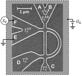
Figure 1:
Scanning electron micrograph of an identically processed sample.
1D waveguides of about 170 nm lithographic width form an asymmetric ring and are connected to narrow 2D electron reservoirs, labeled A to F.
The whole structure is covered by a global top-gate.
, , , and indicate the electron temperature of the 2D reservoirs and indicates the path of the heating current.
and indicate the thermal noise and the gate-voltage, respectively.
Figure 1 shows a scanning electron microscopy image of a device identical to the one investigated in this work.
It was fabricated from an AlGaAs/GaAs heterostructure with a 2DEG 120 nm below the surface, using electron-beam lithography and wet-chemical etching.
The 2D electron density and mobility at K in the dark are cm-2 and cm2/Vs, respectively.
These yield a Fermi wavelength of nm and a mean free path of m.
The 2D electron reservoirs AB and EF are connected with each other via a 1D electron waveguide of 170 nm lithographically defined width.
A narrow 2D channel with 410 m length and 2 m width (lower inset of Fig. 2), fabricated from the same wafer material, was used to investigate thermal noise in a 2DEG of this heterostructure.
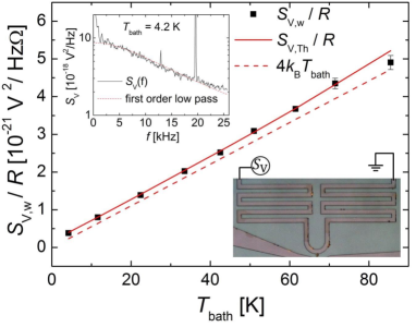
Figure 2:
Measurements of the (reduced) thermal noise at different bath temperatures of a 2DEG from the same AlGaAs/GaAs heterostructure as the sample depicted in Fig. 1.
The (black) squares are the values of obtained from the noise spectra, the (red) full line is theoretical calculated from the two-point resistance of the sample using Eq. 2, and the (red) dashed line is the purely thermal noise, .
Lower right inset: optical micrograph of the narrow 2DEG (410 m length; 2 m width) where the measurement was performed.
Upper left inset: noise spectrum at 4.2 K (black line) and the corresponding first-order low-pass fit (red, dashed line) to obtain .
Voltage noise measurements were performed at a bath temperature of K and the noise spectrum was recorded with an Stanford Research Systems model SR785 signal analyzer.
At 4.2 K the 2D electron reservoirs yield a thermal noise of the order of 10-18 V2/Hz, below the resolution of the signal analyzer.
Two Signal Recovery model 5184 low-noise voltage preamplifiers (gain: 103) were used to increase the thermal noise signal.
Cross-correlated measurements were applied to reduce noise contributions from the preamplifiers. Sampietro, Fasoli, and Ferrari (1999)
The noise spectra were taken in a frequency range of kHz, where 1/f noise is negligible and each noise spectrum is the average of 500 cross-correlated spectra.
In order to take into account parasitic capacitances, each spectrum was fitted with a first-order low-pass filter:
(1)
from which we determine , the frequency-independent, i. e. ’white’, part of the signal; is the two-point resistance of the sample, the parasitic capacitance and the Boltzmann constant.
The theoretical value of the measured signal is the sum of the thermal noise from the sample, the current-noise of the preamplifiers due to their finite input impedance , and the thermal noise from the leads :
(2)
Here denotes the electron temperature, M, K is the amplifier temperature, and V2/Hz.
Two-point resistance measurements were made by standard lock-in technique using the Stanford Research Systems model SR830 lock-in amplifier (frequency Hz, excitation voltage V), in order to determine .
Figure 2 shows the thermal noise of the narrow 2D channel.
The two-point resistance and the thermal noise of the channel were measured in the temperature range of K; no heating current was applied.
In the range K there is an excellent agreement between the measured and the calculated using Eq. 2.
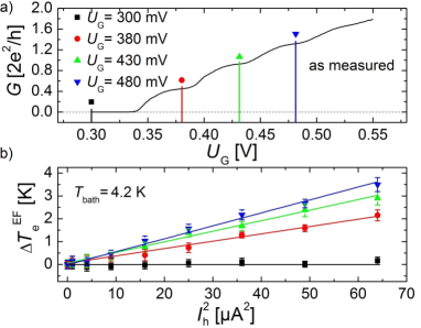
Figure 3 shows the results of the measurements using the setup depicted in Fig. 1.
The noise spectrum in the 2D electron reservoir EF was measured while applying a heating current to the reservoir AB.
was applied using a battery-driven voltage source with low-pass-filters (each formed by a 1 M resistor and a 1 F capacitor) in a “push-pull” configuration.
The top-gate was connected to a similar battery-driven voltage source, also with a low-pass-filter (a 100 k resistor and a 1 F capacitor).
The “low” potential of this battery served as ground.
The electric conductance of the 1D waveguide AB-EF was measured at K in the range V.
The number of populated subbands is given by = 0, 1, 2, and 3 at = 300 mV, 380 mV, 430 mV, and 480 mV, respectively, as depicted in Fig. 3a; means that the 1D waveguide AB-EF is not conducting, i. e. there are no transmitting modes.
For these different occupation numbers, the 2D electron reservoir AB was heated with currents in the range A in steps of 1 A. For each the increase in electron temperature in the 2D reservoir EF was determined from the noise spectrum using the following relation:
(3)
where is the two-point resistance of 2D reservoir EF.
30 minutes after each noise measurement at A, the thermal noise was measured again at A to ensure that reservoir EF had cooled down to .
The results of these thermal measurements are presented in Fig. 3b.
Figure 3:
Results of the thermal measurements at K.
(a) Quantized conductance of the 1D waveguide connecting 2D reservoirs AB and EF, as measured.
The plateaus appear at the gate-voltages 380 mV (red circles), 430 mV (green upward triangles) and 480 mV (blue downward triangles), respectively; at 300 mV (black squares) the 1D waveguide is not conducting.
(b) Increase in electron temperature , calculated using Eq. 3, as a function of heating power at the gate-voltages marked in (a).
Using Eq. 2 to determine at A yields K, depending on ; this is higher than K.
However, this difference does not depend on when is constant, as indicated by the dependence observed in Fig. 3b.
The increased noise acts as a constant offset for constant gate-voltage and is attributed to capacitively-induced potential fluctuations.
Figure 3b shows that increases with only if electrons transmit through 1D waveguide AB-EF, i. e. when .
K for any when , which indicates that electron-phonon interaction at K is not strong enough for a direct heat-exchange between the two 2D reservoirs.
Thus, the 2D reservoirs AB and EF are thermally connected only by the 1D electron waveguide.
For const. the data do not follow the dependence as previously observed for simple QPCs connecting 2D electron reservoirs. van Houten et al. (1992); Chiatti et al. (2006); Jezouin et al. (2013)
To understand this difference, we consider the heat transport in the 1D waveguide network.
In the steady state
(4)
where denotes the heat flow from reservoir AB into the 1D waveguide network, , , and the heat flows into the reservoirs EF, C, and D, respectively, and the heat flow to the lattice due to electron-phonon interaction.
We assume , because the measurement of for in Fig. 3b shows that the electron-phonon interaction can be neglected.
The heat flow through the different paths in the 1D waveguide network can be expressed as follows:
(5)
where describes the increase of the electron temperature over the lattice temperature in reservoir X and is the thermal conductance of the 1D waveguide from reservoir X to reservoir Y.
The reservoirs C and D are on the same side of the ring structure and are separated from reservoirs AB and EF by the same 1D waveguide.
Conductance measurements (see Fig. 4(a) show that , so we can assume that and write .
Defining , the ratio is then
(6)
Applying the Wiedemann-Franz relation yields
(7)
where is the Lorenz number and the electric conductances between reservoirs X and Y.
Combining Eqs. 6 and 7 leads to
(8)
In Fig. 3b it can be seen that for a small heating current, A, the rise in the electron temperature of reservoir EF is much smaller than the lattice temperature, .
So, with , , Eq. 8 becomes
(9)
where is the ratio of the electric two-point conductances between different reservoirs.
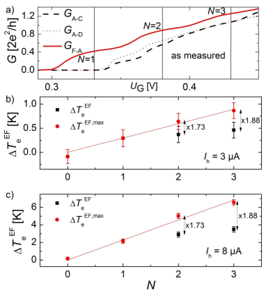
Figure 4:
Comparison of electric conductances and between the measured and calculated with Eq. 15.
(a) Measured conductance between contacts A and F (red, full line), A and D (red, dotted line), and A and C (black, dashed line), corresponding to different 1D waveguides.
The curves are shifted to the left compared to Fig. 3a, because they were measured in a different cooldown; however, the relative position of the curves is the same.
(b) and (c) Increase in electron temperature (black squares) and (red circles) as a function of the number of populated subbands, for A and A, respectively.
The maximum heat flow to the reservoir EF can be estimated by setting
(10)
with
(11)
Here, , because is constant.
Therefore, the heat balance, Eq. 4, can be rewritten using Eqs. 9 and 10 as follows:
and can be replaced using Eqs. 7 and 11, respectively, and we obtain
(14)
The approximation , , yields finally
(15)
Figure 4 shows a comparison between the measured and calculated with Eq. 15.
The electric two-point conductances , and are dominated by the 1D waveguides and were measured to determine for different values of , i. e. for different .
The ratio was found to be for , for , for , and for (see Fig. 4a).
The comparison for A, i. e. for the linear regime, is shown in Fig. 4b.
However, Fig. 4c shows that Eq. 15 holds also for the non-linear regime. Chiatti et al. (2006)
To conclude, the heat flow splits for in the quantum wire network and prevents the observation of , valid for a single QPC. van Houten et al. (1992); Chiatti et al. (2006)
The difference of these results can be explained by taking into account the heat flow along different paths and can be estimated from the electric conductance of the different paths.
The estimate is based on the assumption that the Wiedemann-Franz relation holds van Houten et al. (1992); Chiatti et al. (2006); Jezouin et al. (2013) and the ratio of the electric conductances of the 1D waveguides in the network determines the temperature increase in the reservoir EF.
The top-gate voltage controls which 1D modes carry heat across the structure and therefore allows a selective heating of the 2D reservoirs connected to the quantum wire network.
This has relevance for future applications, such as quantum circuits made of extended electron waveguide networks.
We gratefully acknowledge financial support by the priority programme “Nanostructured thermoelectrics” of the German Science Foundation (DFG) SPP 1386 grant Nr. Fi932/2-2. A. D. W. acknowledges gratefully support of Mercur Pr-2013-0001, BMBF-Q.com-H 16KIS0109, and the DFH/UFA CDFA-05-06. We further thank Dr. Rüdiger Mitdank, Dr. Tobias Kramer and Dr. Christoph Kreisbeck for fruitful scientific discussions.
References
Wees et al. (1988)B. J. Wees, H. van Houten,
C. W. J. Beenakker,
J. G. Williamson,
L. P. Kouwenhoven,
D. van der Marel, and C. T. Foxon, Phys. Rev. Lett. 60, 848 (1988).
Wharam et al. (1988)D. A. Wharam, T. J. Thornton, R. Newbury,
M. Pepper, H. Ahmed, J. E. F. Frost, D. G. H. ans D. C. Peacock, D. A. Ritchie, and G. A. C. Jones, J. Phys. C 21, L209 (1988).
van Houten et al. (1992)H. van
Houten, L. W. Molenkamp, C. W. J. Beenakker, and C. Foxon, Semicond. Sci. Technol. 7, B215 (1992).
Chiatti et al. (2006)O. Chiatti, J. T. Nicholls, Y. Y. Proskuryakov, N. Lumpkin, I. Farrer, and D. A. Ritchie, Phys. Rev. Lett. 97, 056601 (2006).
Jezouin et al. (2013)S. Jezouin, F. D. Parmentier, A. Anthore,
U. Gennser, A. Cavanna, Y. Jin, and F. Pierre, Science 342, 601 (2013).
Sivan and Imry (1986)U. Sivan and Y. Imry, Phys. Rev. B 33, 551 (1986).
Butcher (1990)P. N. Butcher, J.
Phys.: Condens. Matter 2, 4869 (1990).
Buchholz, Sternemann, and Fischer (2012)S. S. Buchholz, E. Sternemann, and S. F. Fischer, Phys.
Rev. B 85, 235301
(2012).
Chiatti et al. (2014)O. Chiatti, S. Buchholz,
U. Kunze, D. Reuter, A. Wieck, and S. Fischer, Phys. Status Solidi B 251, 1753 (2014).
Molenkamp et al. (1990)L. W. Molenkamp, H. van
Houten, C. W. J. Beenakker, R. Eppenga,
and C. Foxon, Appl. Phys.
Lett. 65, 1052 (1990).