Electronic properties of single-layer and multilayer transition metal dichalcogenides MX2 ( Mo, W and S, Se)
Abstract
Single- and few-layer transition metal dichalcogenides have recently emerged as a new family of layered crystals with great interest , not only from the fundamental point of view, but also because of their potential application in ultrathin devices. Here we review the electronic properties of semiconducting , where Mo or W and S or Se. Based on of density functional theory calculations, which include the effect of spin-orbit interaction, we discuss the band structure of single-layer, bilayer and bulk compounds. The band structure of these compounds is highly sensitive to elastic deformations, and we review how strain engineering can be used to manipulate and tune the electronic and optical properties of those materials. We further discuss the effect of disorder and imperfections in the lattice structure and their effect on the optical and transport properties of . The superconducting transition in these compounds, which has been observed experimentally, is analyzed, as well as the different mechanisms proposed so far to explain the pairing. Finally, we include a discussion on the excitonic effects which are present in these systems.
I Introduction
Two-dimensional layered materials are currently being object of great attention due to their physical properties. Single-layer and few-layer graphene have received much attention and bolstered this field of research.Castro-Neto et al. (2009) Recently, the focus is widening to other two-dimensional materials with interesting structural and electronic properties.Britnell et al. (2012) Transition metal dichalcogenides (TMD) form a new family of layered materials that can be easily exfoliated and present promising electrical and optical properties.Novoselov et al. (2005) Among these materials, semiconducting TMD are of special interest since the gap present in both single-layer and multi-layer samples makes them candidates for device applications.Wang et al. (2012); Jariwala et al. (2014); Ganatra and Zhang (2014)
The band structure of those compounds dramatically changes from single-layer to multi-layer samples, involving a transition from a direct gap for single-layer samples to an indirect gap for multi-layer samples,Cappelluti et al. (2013) as it has been observed experimentally,Mak et al. (2010); Zhao et al. (2013); Jin et al. (2013); Zhang et al. (2014) pointing out the important role of interlayer coupling.Castellanos-Gomez et al. (2013a) Furthermore, their electronic properties are highly sensitive to the external conditions such as temperature, pressure or strain. For instance, an insulator/metal transition can be induced under particular conditions.Feng et al. (2012a); Lu et al. (2012); Pan and Zhang (2012); Peelaers and Van de Walle (2012); Scalise et al. (2014, 2012); Yun et al. (2012); Li et al. (2013); Ghorbani-Asl et al. (2013a); Shi et al. (2013); Hromadová et al. (2013); Horzum et al. (2013); Castellanos-Gomez et al. (2013b) This tunability of the gap is very interesting for optoelectronic applications.Wang et al. (2012)
Other important feature of the TMD is the possibility to control quantum degrees of freedom as the electron spin, the valley pseudospin and layer pseudospin.Xu et al. (2014) In fact, the strong spin-orbit interaction in these compounds, and the coupling of the spin, the valley and the layer degrees of freedom opens the possibility to manipulate them for future applications in spintronics and valleytronics devices.Mak et al. (2012, 2013); Cao et al. (2012); Sallen et al. (2012); Xiao et al. (2012); Wu et al. (2013a); Zeng et al. (2012); Ochoa and Roldán (2013) The spin orbit coupling (SOC) lifts the spin degeneracy of the energy bands in single layer samples due to the abscence of inversion symmetry.Zhu et al. (2011) By time reversal symmetry the spin splitting in inequivalent valleys must be opposite, leading to the so called spin-valley coupling,Xiao et al. (2012) which have been observed experimentallyCao et al. (2012); Zeng et al. (2012); Mak et al. (2012); Wu et al. (2013a); Wang et al. (2013); Zeng et al. (2013) and have also been studied theoretically.Feng et al. (2012b); Shan et al. (2013); Rostami et al. (2013); Rose et al. (2013); Liu et al. (2013); Roldán et al. (2014)
Due to the reduced dielectric screening in monolayer and few-layer samples of TMDs, excitonics effects are especially relevant in these compounds. The existence of neutral and charged excitons, as well as their possible manipulation for optoelectronic applications, is attracting a lot of interest from both, experimentalRoss et al. (2013); Mak et al. (2013); Wu et al. (2013b); Jones et al. (2013) and theoreticalRamasubramaniam (2012); Cheiwchanchamnangij and Lambrecht (2012); Berkelbach et al. (2013) points of view.
Similarly as in graphene, metallic behavior can be induced in semiconducting TMD by means of electric field effects or by doping. At high carrier concentrations ( cm-2), and in the presence of high- dielectrics, MoS2 becomes superconductor, with a doping-dependent critical temperature T which exhibits a superconducting dome with a maximum for a certain range of doping and drops to zero at sufficiently large values of ,Taniguchi et al. (2012); Ye et al. (2012) and whose understanding is focus of a number of recent theoretical works.Roldán et al. (2013); Rösner et al. (2014); Yuan et al. (2014); Majidi et al. (2014)
Another topic of current research is the effect of disorder on the optical and electronic properties of TMDs. In particular, the presence of vacancies or adatoms in the samples can modify their mobility, and the importance of short-range disorder is thought as one of the main limitations for the mobility of chemical vapor deposition (CVD) grown single-layer MoS2 Zhu et al. (2014); Schmidt et al. (2014). Theoretically, this problem has been studied using ab initio methods Ataca and Ciraci (2011); Ma et al. (2011); Wei et al. (2012); Komsa and Krasheninnikov (2012); Ghorbani-Asl et al. (2013b); Zhou et al. (2013a); Enyashin et al. (2013); Lanzillo et al. (2013), as well as real space tight-binding (TB) methods which can simulate realistic samples.Yuan et al. (2014)
The present paper analyzes the electronic properties of the group-VIB MX2 (where Mo, W and S, Se). The corresponding band structure for single layer, bilayer and bulk compounds is obtained from density function theory (DFT) calculations, which includes spin-orbit interaction. We discuss the role played by both, the metal and the chalcogen atoms, in the optical and electronic properties of these materials. We review the effects of strain and disorder in the electronic spectrum, as well as the superconducting transition in highly doped samples.
II Electronic structure
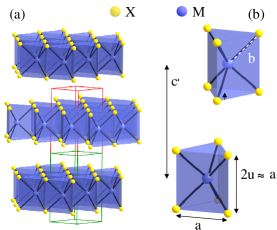
In this section we discuss the main features of the electronic band structure of single-layer, bilayer and bulk TMDs. For this, we will use DFT calculations, including the intrinsic spin-orbit interaction term for all atoms. The crystal structure of single-layer and multilayer MX2 is schematically shown in Fig. 1. The basic unit block of MX2 is composed of an inner layer of atoms on a triangular lattice sandwiched between two layers of atoms lying on the triangular net of alternating hollow sites. We denoteCappelluti et al. (2013) as the distance between nearest neighbor in-plane and distances, as the nearest neighbor distance and as the distance between the and planes. The MX2 crystal forms an almost perfect trigonal prism structure with and very close to the their ideal values and . The experimental values of these lattice distances of the bulk compounds are given in Table 1 for the four materials investigated.Liu et al. (2013); Kośmider et al. (2013); Kumar and Ahluwalia (2012) The in-plane Brillouin zone is thus characterized by the high-symmetry points , K, and M.
| MoS2 | |||
|---|---|---|---|
| WS2 | |||
| MoSe2 | |||
| WSe2 |
| Bandgap | VB(K) | VB() | CB(K) | CB(Q) | |
| Monolayer | |||||
| MoS2 | 1.715 | 0.153 | 0.0041 | 0.0832 | |
| WS2 | 1.659 | 0.439 | 0.0333 | 0.339 | |
| MoSe2 | 1.413 | 0.193 | 0.0258 | 0.0 | |
| WSe2 | 1.444 | 0.439 | 0.0396 | 0.275 | |
| Bilayer | |||||
| MoS2 | 1.710-1.198 | 0.181 | 0.737 | 0.0 | 0.457 |
| WS2 | 1.658-1.338 | 0.451 | 0.677 | 0.0357 | 0.528 |
| MoSe2 | 1.424-1.194 | 0.213 | 0.649 | 0.0253 | 0.417 |
| WSe2 | 1.442-1.299 | 0.454 | 0.649 | 0.0428 | 0.522 |
| Bulk | |||||
| MoS2 | 1.679-0.788 | 0.245 | 1.018 | 0.0 | 0.874 |
| WS2 | 1.636-0.917 | 0.482 | 1.426 | 0.044 | 0.922 |
| MoSe2 | 1.393-0.852 | 0.267 | 0.695 | 0.0228 | 0.819 |
| WSe2 | 1.407-0.910 | 0.504 | 1.075 | 0.0548 | 0.919 |
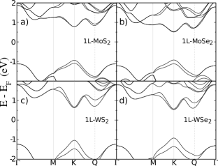
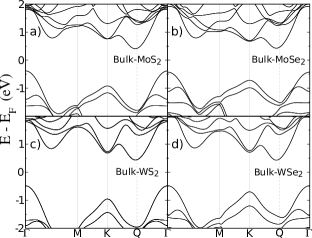
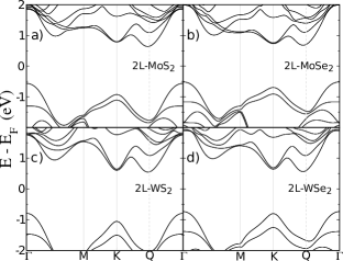
DFT calculations are done using the Siesta code,Soler et al. (2002); Artacho et al. (2008) with the exchange-correlation potential of Ceperly-AlderCeperley and Alder (1980) as parametrized by Perdew and Zunger.Perdew and Zunger (1981) We consider also a split-valence double- basis set including polarization functions.Artacho et al. (1999) The energy cutoff and the Brillouin zone sampling were chosen to converge the total energy with a value of 300 Ry and () in the case of the monolayer and bilayer (bulk), respectively. The energy cutoff was set to eV. We account for the spin-orbit interaction of the different compounds following the method developed in Ref. Fernández-Seivane et al., 2006 Figs. 2-3 show the obtained band structures for single-layer, bilayer and bulk samples of . The lattice parameters used in this calculation are given in Table 1. In Table 2 we summarize the most important features of the band structures calculated in this work, like the energy gaps and the splitting of the valence and conduction bands at different points of the BZ. In Tables 3 and 4 we list details of the band structure of different TMDs obtained in other works in the bibliography. A detailed description of the orbital character of the bands can be found in Ref. Cappelluti et al., 2013. The valence and conduction bands are made by hybridization of the , and orbitals of the transition metal , and the , and orbitals of the chalcogen atoms . All the single-layer compounds shown in Fig. 2 are direct gap semiconductors, with the gap lying at the two inequivalent K points of the hexagonal BZ. The most important orbital contribution at the edge of the valence band at the K point is due to a combination of and of the metal , which hybridize to and orbitals of the chalcogen atoms . On the other hand, the edge of the conduction band has a main contribution due to of , plus a minor contribution of and orbitals of .Cappelluti et al. (2013)
| LDA | GGA | HSE | GW | Exp | |
| Monolayer | |||||
| MoS2 | 1.79Kadantsev and Hawrylak (2012)/1.89Kumar and Ahluwalia (2012)/1.76Huang et al. (2014a)/1.86Ding et al. (2011) | 1.60Ramasubramaniam (2012)/1.59Huang et al. (2014a)/1.67Ding et al. (2011) | 2.05Ramasubramaniam (2012)/2.32Ellis et al. (2011)/1.786Zahid et al. (2013)/2.25Ding et al. (2011) | 2.82Ramasubramaniam (2012)/2.759Cheiwchanchamnangij and Lambrecht (2012)/2.41Molina-Sánchez et al. (2013)/2.66Ding et al. (2011) | 1.8Sahin et al. (2013); Splendiani et al. (2010)/1.90Mak et al. (2010)/1.86Eknapakul et al. (2014) |
| WS2 | 2.05Kumar and Ahluwalia (2012)/1.94Ding et al. (2011) | 1.56Ramasubramaniam (2012)/1.80Ma et al. (2011)/2.1Kuc et al. (2011)/1.9 | 1.87Ramasubramaniam (2012)?/1.81Ding et al. (2011) | 2.88Ramasubramaniam (2012)/2.32Ding et al. (2011) | 2.91Ding et al. (2011) |
| MoSe2 | 1.58Kumar and Ahluwalia (2012)/1.63Ding et al. (2011) | 1.35Ramasubramaniam (2012)/1.44Ma et al. (2011)/1.44Ding et al. (2011) | 1.75Ramasubramaniam (2012)/1.99Ding et al. (2011) | 2.41Ramasubramaniam (2012)/2.31Ding et al. (2011) | 1.76Lebègue and Eriksson (2009)/1.58Zhang et al. (2014)/1.55Tongay et al. (2012) |
| WSe2 | 1.61Kumar and Ahluwalia (2012)/1.45Huang et al. (2014a)/1.74Ding et al. (2011) | 1.19Ramasubramaniam (2012)/1.25Sahin et al. (2013)/1.32Zeng et al. (2013)/1.19Huang et al. (2014a) /1.55Ding et al. (2011) | 1.68Ramasubramaniam (2012)/2.10Ding et al. (2011) | 2.42(Indirect!)Ramasubramaniam (2012)/2.51Ding et al. (2011) | 1.64Sahin et al. (2013)/1.64Zeng et al. (2013) |
| Bilayer | |||||
| MoS2 | 1.68Molina-Sánchez et al. (2013)/1.75-1.17Huang et al. (2014a) | 1.275Ramasubramaniam et al. (2011)/1.56-1.17Huang et al. (2014a) | 1.9Ellis et al. (2011)/1.480Zahid et al. (2013)( to K) | 1.888Cheiwchanchamnangij and Lambrecht (2012)/2.32Molina-Sánchez et al. (2013)/1.18( to K)Zhao et al. (2013) | 1.88/1.6Mak et al. (2010)/1.51Zhao et al. (2013) |
| WS2 | - | 1.37Ramasubramaniam et al. (2011) | - | - | 1.7Zhao et al. (2013) |
| MoSe2 | 1.12Ramasubramaniam et al. (2011) | ||||
| WSe2 | 1.35Kumar and Ahluwalia (2012)/1.68-1.27Huang et al. (2014a) | 1.23Sahin et al. (2013)/1.1Zhao et al. (2013)/1.41-1.12Zeng et al. (2013)/1.19-1.14Huang et al. (2014a) | - | - | 1.5Zhao et al. (2013)/1.59-1.51Zeng et al. (2013) |
| Bulk | |||||
| MoS2 | 1.67Molina-Sánchez et al. (2013)/0.75Kumar and Ahluwalia (2012)/1.71-0.72Huang et al. (2014a) | 1.55-0.92Huang et al. (2014a)/1.62-0.88Jiang (2012) | 1.37Ellis et al. (2011)/1.328Zahid et al. (2013) | 1.287Cheiwchanchamnangij and Lambrecht (2012)/2.23Molina-Sánchez et al. (2013)/2.07-1.23Jiang (2012) | 1.8/1.29Mak et al. (2010)/1.23Kam and Parkinson (1982)/1.29Böker et al. (2001) |
| WS2 | 0.89Kumar and Ahluwalia (2012) | 1.21Sahin et al. (2013)/1.65-0.94Jiang (2012) | - | 2.13-1.30Jiang (2012) | 1.57Sahin et al. (2013)/1.35Kam and Parkinson (1982) |
| MoSe2 | 0.80Kumar and Ahluwalia (2012) | 1.39-0.84Jiang (2012) | - | 1.83-1.11Jiang (2012) | 1.09Kam and Parkinson (1982)/1.1Böker et al. (2001) |
| WSe2 | 0.97Kumar and Ahluwalia (2012) | 1.5-0.81Huang et al. (2014a)/1.33-0.92Jiang (2012) | - | 1.75-1.19Jiang (2012) | 1.2Kam and Parkinson (1982)/1.60-1.44Zeng et al. (2013) |
The main difference between the Mo [Fig. 2(a) and (b)] and W [Fig. 2(c) and (d)] compounds is observed in the splitting of the valence band for each case, which is due to SOC. Whereas for the Mo compounds it is of the order of 150 meV, for the heavier W compounds increases up to 400 meV. SOC also lead to a splitting of the conduction band at both, the band edge at the K point,Kośmider et al. (2013) as well as at the secondary minimum Q which lies between the and K points of the BZ (indicated in Fig. 2-3 by a dashed vertical line). Notice that, since Q is not a high symmetry point of the BZ, the minima of the conduction band for bilayer and bulk materials do not lie exactly at the same point than for single layers. This is why the minima of the conduction band in Figs. 4 and 3 are slightly shifted with respect to the single-layer Q point.
For monolayer samples and around the K and K’ points, it is possible to assign a spin projection to the different Bloch states along the normal to the plane. It is possible to define a sign for the SOC induced splitting of the band from the difference . Time reversal symmetry implies that , leading to splitting of opposite sign at the K and K’ points. DFT calculations show, for the K point of the conduction band, a negative sign for for the Mo compounds ( meV for MoS2 and meV for MoSe2) and a positive sign for the W compounds ( meV for WS2 and meV for WSe2).Kośmider et al. (2013) Notice that the SOC splitting of the conduction band is larger for the Se compounds as compared to the S compounds. This is expected due to the heavier mass of selenium as compared to sulfur. Since the orbital weight of the and orbitals of chalcogen atoms at the K point of the conduction band is of the order of ,Cappelluti et al. (2013) first order processes associated to this atoms lead to a contribution to the SOC splitting, being more noticeable for the Se compounds. Recent calculations suggest that Coulomb interaction can modify the SOC split bands.Ferreiros and Cortijo (2014)
| LDA | GGA | FPLAPW | HSE | GW | Exp | |
| Monolayer | ||||||
| MoS2 | 0.1901Kadantsev and Hawrylak (2012) | 0.147Sahin et al. (2013)/0.146Ramasubramaniam (2012)/0.147Kośmider et al. (2013) | 0.148Zhu et al. (2011) | 0.193Ramasubramaniam (2012)/0.188Zahid et al. (2013) | 0.164Ramasubramaniam (2012)/0.146Cheiwchanchamnangij and Lambrecht (2012)/0.112Molina-Sánchez et al. (2013) | 0.150Mak et al. (2010)/0.170Ramasubramaniam (2012) |
| WS2 | - | 0.435 Sahin et al. (2013)/0.425Ramasubramaniam (2012)/0.433Kośmider et al. (2013) | 0.426Zhu et al. (2011) | 0.521Ramasubramaniam (2012) | 0.456Ramasubramaniam (2012) | - |
| MoSe2 | - | 0.183Ramasubramaniam (2012)/0.186Kośmider et al. (2013) | 0.183Zhu et al. (2011) | 0.261Ramasubramaniam (2012) | 0.26Ramasubramaniam (2012) | 0.180Zhang et al. (2014) |
| WSe2 | - | 0.461Ramasubramaniam (2012)/0.463Kośmider et al. (2013)/0.43Zeng et al. (2013) | 0.456Zhu et al. (2011) | 0.586Ramasubramaniam (2012) | 0.501Ramasubramaniam (2012) | - |
| Bilayer | ||||||
| MoS2 | 0.1738Molina-Sánchez et al. (2013) | 0.17Ramasubramaniam et al. (2011) | - | 0.201Zahid et al. (2013) | 0.174Cheiwchanchamnangij and Lambrecht (2012)/0.160Molina-Sánchez et al. (2013) | 0.170Mak et al. (2010) |
| WS2 | - | - | - | - | - | - |
| MoSe2 | - | - | - | - | - | - |
| WSe2 | - | 0.43Zeng et al. (2013) | - | - | - | - |
| Bulk | ||||||
| MoS2 | 0.2201Molina-Sánchez et al. (2013)/0.258Böker et al. (2001) | 0.23Ramasubramaniam et al. (2011) | 0.184Zahid et al. (2013) | 0.238Cheiwchanchamnangij and Lambrecht (2012)/0.2306Molina-Sánchez et al. (2013) | - | 0.180Mak et al. (2010)/0.161Böker et al. (2001) |
| WS2 | - | - | - | - | - | - |
| MoSe2 | 0.294Böker et al. (2001) | - | - | - | 0.175Böker et al. (2001) | - |
| WSe2 | - | - | - | - | - | - |
III Effect of strain
The phonon structure of TMDs considered here is highly sensitive to strain. The Raman spectra of these compounds contain two main peaks which correspond to the A1g out-of-plane mode, where the top and bottom atoms are moving out of plane in opposite directions while is fixed, and the in-plane mode where the and atoms are moving in-plane in opposite directions.Molina-Sánchez and Wirtz (2011); Lee et al. (2010) These phonon modes are red shifted with increasing temperatures, which might point the importance of anharmonic contributions to the interatomic potentials.Lanzillo et al. (2013) The mode is very sensitive to applied strain. Applying uniaxial strain lifts the degeneracy of this mode, leading to red shifting and splitting into two distinct peaks for strain of just 1%.Castellanos-Gomez et al. (2013b); Conley et al. (2013); Hui et al. (2013) The particular electronic structure and phonon modes of TMDs suggest that band structure engineering methods can be used for electronic and optoelectronic applications. This technique can be especially useful for TMDs which have been shown to sustain elastically deformations up to 11% without breaking the material.Castellanos-Gómez et al. (2012)
Furthermore, the SOC induces a finite band splitting in single-layer systems also at the six inequivalent valleys at the Q point of the BZ,Zhu et al. (2011); Roldán et al. (2014) with the corresponding entanglement of spin/valley/orbital degrees of freedom.Yuan et al. (2014) At the microscopic level, we remind that the main orbital character of the conduction bands at the Q point is due to a roughly equal distribution of the and orbitals of the transition metal , and of the and orbitals of the chalcogen atom . The rather large contribution from both - and -orbitals leads to a strong hybridization between and atoms at this Q point of the BZ. This makes these states highly sensitive to uniform and local strains and lattice distortions.Castellanos-Gomez et al. (2013b) In fact, since the minimum of the conduction band at Q becomes the effective band edge in bilayer and multilayer samples (see Figs. 4 and 3), this suggests that the states at the minima of the conduction band at the Q are good candidates for tuning the spin/orbital/valley entanglement in these materials by means of strain engineeringCastellanos-Gomez et al. (2013b) or (in multilayer systems) by means of electric fields.Wu et al. (2013a)
The application of forces across specific axes of the crystal structure induces strain in the sample which, at the same time, can be used to modify the band structure of TMDs. A reduction of the band gap can be achieved under uniaxial compressive strain across the -axis of the crystal structure of .Peelaers and Van de Walle (2012) On the other hand, biaxial tensile strain makes the minimum of the conduction band at the Q point to move upward, while the conduction band at the K point moves downward with no significant effect in the valence band at the point. Furthermore, tensile strain is expected to lower the electron effective massShi et al. (2013) and consequently improve electron mobility, and could also lead to band degeneracy. Some of these theoretical results have been confirmed by strain experiments in single layer and multi-layer , which shows a change in the band gap up to meV per 1% applied strain.Hui et al. (2013); Conley et al. (2013); Castellanos-Gomez et al. (2013b) Strain can be induced by depositing MoS2 on hexagonal boron nitride (h-BN), which can lead to a direct-to-indirect gap transition, as predicted by first-principle calculations.Huang et al. (2014b) Recent proposals suggest that time-reversal invariant topological phases in TMDs can be engineered by application of strain.Cazalilla et al. (2014)
Of special interest is the use of strain engineering on to create a broad-band optical funnel. This idea, proposed theoretically by Feng et al.Feng et al. (2012a) and confirmed experimentally by Castellanos-Gomez et al.Castellanos-Gomez et al. (2013b) consists on continuously change the strain across a sheet of monolayer MoS2, leading to a continuous variation of the optical band gap, which allows not only the capture of photons across a wide range of the solar spectrum, but also guidance of the resulting generated excitons toward contacts.
IV Effect of disorder
Disorder in the lattice structure, such as adatoms or vacancies, can strongly modify the optical and transport properties of materials. In particular the mobility of TMDs is highly dependent on the screening environment and is limited by the presence of impurities in the samples.Kaasbjerg et al. (2012); Jariwala et al. (2013); Sangwan et al. (2013); Kaasbjerg et al. (2013) Experimental results show that the optical and transport properties of these materials can be influenced by the existence of defects in their chemical and structural composition. Vacancies in crystals trap free charge carriers and localize excitons, leading to new peaks in the photoluminescence spectra.Tongay et al. (2013) Such vacancies can be created by means of thermal annealing and -particle Tongay et al. (2013) or electron beam irradiation.Zhou et al. (2013b) The optical spectrum of bilayer MoS2 presents a broad peak at eV which has been associated to impurities,Wu et al. (2013a) whereas the mobility of multilayer samples has been shown to highly depend on the substrate and dielectric effects.Bao et al. (2013) Line defects, which separate patches or islands where the layer direction is opposite to its surrounding, can lead to changes in the carrier mobility.Enyashin et al. (2013) Furthermore, short-range scatterers have been proposed as the main limitation for the mobility of chemical vapor deposition (CVD) grown single-layer MoS2.Zhu et al. (2014); Schmidt et al. (2014) Recent scanning tunneling microscopy (STM) and scanning tunneling spectroscopy (STS) in combination with transport measurements suggest that the intrinsic -doping in bulk MoS2 is due to point defects which are consistent with S vacancies. Moreover, the significantly higher -doping observed in thin films deposited on SiO2 is extrinsic and has been attributed to trapped donors at the interface with the SiO2 substrate.Lu et al. (2014) The controlled creation of defects could be exploited as a route to manipulate the electronic properties of these materials.
On the theoretical ground, the effect of disorder has been first studied using DFT methods. Ataca and Ciraci (2011); Ma et al. (2011); Wei et al. (2012); Komsa and Krasheninnikov (2012); Ghorbani-Asl et al. (2013a); Zhou et al. (2013a); Enyashin et al. (2013); Lanzillo et al. (2013) The study of adsorption of adatoms and creation of vacancy defects in MoS2 nanoribbons have shown that a net magnetic moment can be achieved through the adsorption of Co adatoms to the non-magnetic armchair nanoribbons. Furthermore, apart from the spin-polarization, significant charges can be transferred to (or from) the adatom.Ataca and Ciraci (2011) Spin-polarized DFT calculations for MoS2 antidots show that the net spin and the stability of spin states can be engineered by controlling the type and distance of internal nanoholes. The case of only S-terminated antidots is found that can exhibit a large net spin above room temperature.Zhou et al. (2013a)
The electronic and optical properties of single-layers of MoS2 and WS2 in the presence of vacancies have been also studied within a real space tight-binding (TB) model for large systems, containing millions of atoms, by solving the time-dependent Schrödinger equation, and by means of numerically exact Kubo formula calculations.Yuan et al. (2014) Vacancies induce states in the middle of the gap whose energy depends on the specific vacant atoms, and the optical transitions involving the impurity bands lead to a background contribution in the optical conductivity at low energies, which has been proposed to be behind the features observed in photoconductivity experiments.Mak et al. (2010) samples also show a significant asymmetry between electrons and holes,Bao et al. (2013) such that the DC conductivities and mobilities are larger for holes. When comparing the S2 compounds, it is found higher mobilities for -doped WS2 than for MoS2.Yuan et al. (2014)
V Spin/valley/layer coupling
In single layers of , the lack of inversion symmetry as well as the SOC leads to a break in spin degeneracy along both, the valence and conduction bands, and also causes valley Hall effect where carriers flow into opposite transverse edges upon application of an in-plane electric field.Cao et al. (2012); Zeng et al. (2012); Lu et al. (2013); Mak et al. (2014) In addition, time reversal symmetry of the single layers of together with non degeneracy of the spin energy bands lead to a coupling of spin and valley states.Xiao et al. (2012) This results in valley-dependent optical polarization selection for individual valleys. Since time reversal symmetry forces opposite spin-splitting at each valley, such effect can be used to control the valley polarization by means of optical helicity,Mak et al. (2012) such that the K valley would correspond to optical selection rules of a certain helicity as well as carriers of a fixed spin, while the K’ valley would correspond to opposite conditions. This makes possible to control carrier spin as well as carrier confinement within a specific valley with circularly polarized light, an effect that has been observed experimentally.Mak et al. (2012); Zeng et al. (2012); Cao et al. (2012) Since inter-valley scattering is in principle forbidden due to the breaking of spin degeneracy, this suggests long spin lifetimes in single layers of . As a matter of fact, spin lifetimes larger than 1 ns have been determined experimentally,Mak et al. (2012) in agreement with theoretical calculations for intravalley SOC mediated spin relaxation in MoS2.Ochoa and Roldán (2013) In the absence of defects, spin relaxation of the carriers is also possible due to flexural deformations of the samples.Ochoa et al. (2013)
New interesting features are present in bilayers of , which consists on a stack of two single layers in-plane rotated by with respect to each other, bound by means of weak van der Waals interactions. The inter-layer hopping of electrons between different layers leads to a strong modification of the band structure, driving a transition from a direct gap semiconductor in single-layer systems to an indirect gap semiconductor in bilayer compounds, as it can be seen by comparing Fig. 2 and 4. The inter-layer hopping, which links mainly the orbitals of the chalcogen atoms of different layers,Cappelluti et al. (2013) lead to a splitting of the maximum of the valence band at the point, which becomes the effective valence band edge, as well as a splitting of the minimum of the conduction band at the Q point, which becomes the absolute minimum of the conduction band.Roldán et al. (2014)
Contrary to single-layer MX2, bilayer MX2 presents point-center inversion symmetry.Wu et al. (2013a); Gong et al. (2013); Zeng et al. (2013) Therefore, the band structure of bilayer remains spin degenerate even in the presence of SOC. However, since the SOC does not couple orbitals of different layers, each single band preserves a finite entanglement between spin, valley and the layer index. Such spin-valley-layer coupling can be observed at the K point of the valence band,Gong et al. (2013), as well as at the conduction band.Roldán et al. (2014) This last case can be of special interest for slightly electron-doped bilayer , whose Fermi surface presents six pockets centered at the inequivalent Q valleys of the BZ, and no pockets at the K and K’ valleys. Of special interest are the families of TMDs with stronger spin-orbit interaction, like WS2 and WSe2, for which the SOC can be larger than the inter-layer hopping, enhancing the spin/layer/valley entanglement. Then, although inversion symmetry forces each Fermi pocket to be spin degenerate, the layer polarization makes that each layer contributes with opposite spin in alternating valleys. This effect can be useful for valleytronics devices. The importance of spin and valley states was proven by optical probes in bilayer MoS2, obtaining a reduction of the photoluminescence by more than 20 times, and hole spin lifetime was 3 orders smaller than those observed in single layers of MoS2.Mak et al. (2012) The control and tuning of circularly polarized photoluminescence from bilayer MoS2 can be achieved with the application of a gate voltage, which breaks inversion symmetry due to the electric field, as it has been shown by recent experiments.Wu et al. (2013a)
VI Excitons
The additional spin-like quantum numbers discussed in Sec. V play an important role in the physics of excitons in TMDs. The reduced dielectric screening in monolayer and few layer samples suggest that strong excitonic effects should appear in these materials. In fact, the existence of highly stable neutral and charged excitons has been proven experimentally.Ross et al. (2013); Mak et al. (2013); Jones et al. (2013) In those experiments, optically excited electrons and holes are bound together by means of Coulomb interaction. Contrary to excitons in conventional semiconductors as GaAs, for which the excitons form at the point of the BZ, excitons in TMDs occur at the K and K’ points of the BZ, leading to the so called valley excitons, which open new opportunities to manipulate and control the valley index by means of optical probes, as we have discussed in the previous section. The large SOC splitting of the valence band at the K point leads to two excitonic features in the photo-absorption spectrum,Mak et al. (2010) usually denoted as the A and B excitons. On the other hand, the binding energy of the charged excitons (usually called trions) is unexpectedly large (18 meV for MoS2,Mak et al. (2013) and 30 meV for both MoSe2,Ross et al. (2013) and WSe2Jones et al. (2013)), pointing out that Coulomb interactions are very strong in these families of layered TMDs.
A large exciton binding energy (0.32 eV) and a significant deviation from the conventional hydrogenic model, typically used to describe the Wannier excitons in inorganic semiconductors, has been found in the full sequence of excited (Rydberg) exciton states in monolayer and few-layer WS2, measured by optical reflexion experiments.Chernikov et al. (2014) A theoretical microscopic model that considers the modification of the functional form of the Coulomb interaction due to the nonlocal nature of the effective dielectric screening has been successfully applied to explain these unusually strong electron-hole interactions.Chernikov et al. (2014)
To tackle this problem using first principle methods, one needs to go beyond DFT calculations since it is well know that Kohn-Sham energies do not correspond to quasiparticle energies. A better route is to consider approximation in conjunction with Bethe-Salpeter equation (BSE) to consider the two-particle excitations.Cheiwchanchamnangij and Lambrecht (2012); Ramasubramaniam (2012) Other possibility is to use an effective mass model (parametrized by ab initio calculations), and including appropriate screening of the interactions for quasi-2D semiconductors.Berkelbach et al. (2013) The separation between the excitons is directly related to the strength of the SOC splitting of the valence band, and excitation energies in the range 1 to 2 eV have been predicted,Ramasubramaniam (2012) suggesting a potential application of TMDs for optoelectronic devices in the near-IR to the red regime. In Table 5 we list the binding energies of the neutral excitons obtained theoretically from different approximations, as well some experimental values that have been reported in the literature.
| Monolayer | Bilayer | Bulk | |||||
|---|---|---|---|---|---|---|---|
| Effective model | GW | GW | Exp. | GW | |||
| MoS2 | 0.54Berkelbach et al. (2013) | 0.897Cheiwchanchamnangij and Lambrecht (2012)/1.03Ramasubramaniam (2012)/1.1Komsa and Krasheninnikov (2012)/0.5Feng et al. (2012a)/0.54Shi et al. (2013) | 0.424Cheiwchanchamnangij and Lambrecht (2012) | 0.08Komsa and Krasheninnikov (2012) | 0.13Komsa and Krasheninnikov (2012)/0.025Cheiwchanchamnangij and Lambrecht (2012) | ||
| WS2 | 0.47Berkelbach et al. (2013) | 0.91Ramasubramaniam (2012) | - | - | - | ||
| MoSe2 | 0.50Berkelbach et al. (2013) | 1.04Ramasubramaniam (2012)/0.54(Shi et al., 2013) | - | 0.07Komsa and Krasheninnikov (2012) | 0.11Komsa and Krasheninnikov (2012) | ||
| WSe2 | 0.42Berkelbach et al. (2013) | 0.90Ramasubramaniam (2012) | - | - | - | ||
VII Superconductivity
Another interesting aspect of the TMDs is the appearance of a superconducting transition with a critical temperature that strongly depends on the carrier density. A superconducting dome, similar to that observed for the layered cuprate, has been experimentally observed in the temperature-carrier density phase diagram of MoS2,Ye et al. (2012); Taniguchi et al. (2012) in which the samples were doped by a combination of liquid and solid gating. For the optimal doping the critical temperature is of K.
Theoretically, the origin of superconductivity in heavily doped MoS2 was first studied in Ref. Roldán et al., 2013, by considering the role of both electron-electron and electron-phonon interactions. The estimations for the strength of the different contributions to the effective coupling suggest that superconductivity in MoS2, under the experimental conditions of Refs. Taniguchi et al., 2012 and Ye et al., 2012, is likely to be induced by the electron-electron interaction. The significant short-range repulsion between carriers at the conduction band allows for a superconducting phase induced by the electron-electron interaction with a nontrivial structure, where the gap acquires opposite signs in the two inequivalent pockets of the conduction band. On the other hand, DFT calculations for the phase diagram of TMDs suggest that phonon mediated superconductivity is also possible for some range of electron doping, and a charge density wave is also proposed to exist for even higher carrier concentrations.Rösner et al. (2014) Recently it has been suggested that spin-triplet -wave superconductivity can be stabilized by Rashba SOC in MoS2.Yuan et al. (2014) Finally, the superconducting proximity effect and the Andreev reflection in superconducting-normal (S/N) hybrid junction with n- (p-)doped S and p-doped N regions has been investigated in Ref. Majidi et al., 2014, finding that the strong SOC enhances the Andreev conductance of the MoS2-based S/N structure relative to its value in the corresponding structure with gapped graphene.
VIII Conclusions
In conclusion, we have discussed the electronic properties of semiconducting TMDs , where and . DFT band structure calculations, including the effect of SOC, have been used to discuss the differences between the single layer, bilayer and bulk compounds. The splitting of the bands due to SOC has been discussed in the whole BZ, analyzing the role of the transition metal and the chalcogen atoms at each relevant point of the band structure. We have further reviewed the effect of strain in the samples, discussing how strain engineering is a good route to manipulate and tune the electronic and optical properties of those compounds. Disorder and imperfections in the lattice structure lead to the creation of impurity states in the middle of the gap, which contribute to the photoconductivity. Finally, we have discussed the superconducting phase which has been also experimentally observed in the TMDs, and which present a superconducting dome in the temperature-carrier density phase diagram, which resembles to that of the cuprate superconductors. The different mechanisms proposed to explain the superconducting pairing have been reviewed.
Acknowledgements.
R.R., M.P.L.-S. and F.G. acknowledge financial support from MINECO, Spain, through grant FIS2011-23713, and the European Union, through grant 290846. R. R. acknowledges financial support from the Juan de la Cierva Program (MINECO, Spain). E.C. acknowledges support from the European project FP7-PEOPLE-2013-CIG “LSIE_2D” and Italian National Miur Prin project 20105ZZTSE. J.A.S.-G. and P.O. ackowledge support from Spanish MINECO (Grants No. FIS2012-37549-C05-02 with joint financing by FEDER Funds from the European Union, and No. CSD2007-00050) and to Generalitat de Catalunya (2014 SGR 301). J.A.S.-G. was supported by an FPI Fellowship from MINECO. The authors thankfully acknowledges the computer resources, technical expertise and assistance provided by the Red Española de Supercomputación.References
- Castro-Neto et al. (2009) A. H. Castro-Neto, F. Guinea, N. M. R. Peres, K. S. Novoselov, and A. K. Geim, Rev. Mod. Phys. 81, 109 (2009).
- Britnell et al. (2012) L. Britnell, R. Gorbachev, R. Jalil, B. Belle, F. Schedin, A. Mishchenko, T. Georgiou, M. Katsnelson, L. Eaves, S. Morozov, et al., Science 335, 947 (2012).
- Novoselov et al. (2005) K. S. Novoselov, D. Jiang, F. Schedin, T. J. Booth, V. V. Khotkevich, S. V. Morozov, and A. K. Geim, Proc. Natl. Acad. Sci. USA 102, 10451 (2005).
- Wang et al. (2012) Q. H. Wang, K. Kalantar-Zadeh, A. Kis, J. N. Coleman, and M. S. Strano, Nature Nanotech. 7, 699 (2012).
- Jariwala et al. (2014) D. Jariwala, V. K. Sangwan, L. J. Lauhon, T. J. Marks, and M. C. Hersam, ACS Nano 8, 1102 (2014).
- Ganatra and Zhang (2014) R. Ganatra and Q. Zhang, ACS Nano 8, 4074 (2014).
- Cappelluti et al. (2013) E. Cappelluti, R. Roldán, J. A. Silva-Guillén, P. Ordejón, and F. Guinea, Phys. Rev. B 88, 075409 (2013).
- Mak et al. (2010) K. F. Mak, C. Lee, J. Hone, J. Shan, and T. F. Heinz, Phys. Rev. Lett. 105, 136805 (2010).
- Zhao et al. (2013) W. Zhao, R. M. Ribeiro, M. Toh, A. Carvalho, C. Kloc, A. H. Castro Neto, and G. Eda, Nano Letters 13, 5627 (2013).
- Jin et al. (2013) W. Jin, P.-C. Yeh, N. Zaki, D. Zhang, J. T. Sadowski, A. Al-Mahboob, A. M. van der Zande, D. A. Chenet, J. I. Dadap, I. P. Herman, et al., Phys. Rev. Lett. 111, 106801 (2013).
- Zhang et al. (2014) Y. Zhang, T.-R. Chang, B. Zhou, Y.-T. Cui, H. Yan, Z. Liu, F. Schmitt, J. Lee, R. Moore, Y. Chen, et al., Nature Nanotechnology 9, 111 (2014).
- Castellanos-Gomez et al. (2013a) A. Castellanos-Gomez, E. Cappelluti, R. Roldán, N. Agraït, F. Guinea, and G. Rubio-Bollinger, Advanced Materials 25, 899 (2013a).
- Feng et al. (2012a) J. Feng, X. Qian, C.-W. Huang, and J. Li, Nature Photonics 6, 866 (2012a).
- Lu et al. (2012) P. Lu, X. Wu, W. Guo, and X. C. Zeng, Physical Chemistry Chemical Physics 14, 13035 (2012).
- Pan and Zhang (2012) H. Pan and Y.-W. Zhang, The Journal of Physical Chemistry C 116, 11752 (2012).
- Peelaers and Van de Walle (2012) H. Peelaers and C. G. Van de Walle, Phys. Rev. B 86, 241401 (2012).
- Scalise et al. (2014) E. Scalise, M. Houssa, G. Pourtois, V. Afanas?ev, and A. Stesmans, Physica E: Low-dimensional Systems and Nanostructures 56, 416 (2014).
- Scalise et al. (2012) E. Scalise, M. Houssa, G. Pourtois, V. Afanas ev, and A. Stesmans, Nano Research 5, 43 (2012).
- Yun et al. (2012) W. S. Yun, S. Han, S. C. Hong, I. G. Kim, and J. Lee, Phys. Rev. B 85, 033305 (2012).
- Li et al. (2013) Y. Li, Y.-L. Li, C. M. Araujo, W. Luo, and R. Ahuja, Catal. Sci. Technol. 3, 2214 (2013).
- Ghorbani-Asl et al. (2013a) M. Ghorbani-Asl, S. Borini, A. Kuc, and T. Heine, Phys. Rev. B 87, 235434 (2013a).
- Shi et al. (2013) H. Shi, H. Pan, Y.-W. Zhang, and B. I. Yakobson, Phys. Rev. B 87, 155304 (2013).
- Hromadová et al. (2013) L. Hromadová, R. Martoňák, and E. Tosatti, Phys. Rev. B 87, 144105 (2013).
- Horzum et al. (2013) S. Horzum, H. Sahin, S. Cahangirov, P. Cudazzo, A. Rubio, T. Serin, and F. M. Peeters, Phys. Rev. B 87, 125415 (2013).
- Castellanos-Gomez et al. (2013b) A. Castellanos-Gomez, R. Roldán, E. Cappelluti, M. Buscema, F. Guinea, H. S. J. van der Zant, and G. A. Steele, Nano Letters 13, 5361 (2013b).
- Xu et al. (2014) X. Xu, W. Yao, D. Xiao, and T. F. Heinz, Nature Physics 10, 343 (2014).
- Mak et al. (2012) K. F. Mak, K. He, J. Sahn, and T. F. Heinz, Nature Nanotech. 7, 494 (2012).
- Mak et al. (2013) K. F. Mak, K. He, C. Lee, G. H. Lee, J. Hone, T. F. Heinz, and J. Shan, Nature Mat. 12, 207 (2013).
- Cao et al. (2012) T. Cao, G. Wang, W. Han, H. Ye, C. Zhu, J. Shi, Q. Niu, P. Tan, E. Wang, B. Liu, et al., Nature Commun. 3, 887 (2012).
- Sallen et al. (2012) G. Sallen, L. Bouet, X. Marie, G. Wang, C. R. Zhu, W. P. Han, Y. Lu, P. H. Tan, T. Amand, B. L. Liu, et al., Phys. Rev. B 86, 081301 (2012).
- Xiao et al. (2012) D. Xiao, G.-B. Liu, W. Feng, X. Xu, and W. Yao, Phys. Rev. Lett. 108, 196802 (2012).
- Wu et al. (2013a) S. Wu, J. S. Ross, G.-B. Liu, G. Aivazian, A. Jones, Z. Fei, W. Zhu, D. Xiao, W. Yao, D. Cobden, et al., Nature Physics 9, 149 (2013a).
- Zeng et al. (2012) H. Zeng, J. Dai, W. Yao, D. Xiao, and X. Cui, Nature Nanotech. 7, 490 (2012).
- Ochoa and Roldán (2013) H. Ochoa and R. Roldán, Phys. Rev. B 87, 245421 (2013).
- Zhu et al. (2011) Z. Y. Zhu, Y. C. Cheng, and U. Schwingenschlögl, Phys. Rev. B 84, 153402 (2011).
- Wang et al. (2013) Q. Wang, S. Ge, X. Li, J. Qiu, Y. Ji, J. Feng, and D. Sun, ACS Nano 7, 11087 (2013).
- Zeng et al. (2013) H. Zeng, G.-B. Liu, J. Dai, Y. Yan, B. Zhu, R. He, L. Xie, S. Xu, X. Chen, W. Yao, et al., Scientific Reports 3, 1608 (2013).
- Feng et al. (2012b) W. Feng, Y. Yao, W. Zhu, J. Zhou, W. Yao, and D. Xiao, Phys. Rev. B 86, 165108 (2012b).
- Shan et al. (2013) W.-Y. Shan, H.-Z. Lu, and D. Xiao, Phys. Rev. B 88, 125301 (2013).
- Rostami et al. (2013) H. Rostami, A. G. Moghaddam, and R. Asgari, Phys. Rev. B 88, 085440 (2013).
- Rose et al. (2013) F. Rose, M. O. Goerbig, and F. Piéchon, Phys. Rev. B 88, 125438 (2013).
- Liu et al. (2013) G.-B. Liu, W.-Y. Shan, Y. Yao, W. Yao, and D. Xiao, Phys. Rev. B 88, 085433 (2013).
- Roldán et al. (2014) R. Roldán, M. López-Sancho, E. Cappelluti, J. Silva-Guillén, P. Ordejón, and F. Guinea, arXiv preprint arXiv:1401.5009 (2014).
- Ross et al. (2013) J. S. Ross, S. Wu, H. Yu, N. J. Ghimire, A. M. Jones, G. Aivazian, J. Yan, D. G. Mandrus, D. Xiao, W. Yao, et al., Nature communications 4, 1474 (2013).
- Wu et al. (2013b) C.-C. Wu, D. Jariwala, V. K. Sangwan, T. J. Marks, M. C. Hersam, and L. J. Lauhon, The Journal of Physical Chemistry Letters 4, 2508 (2013b).
- Jones et al. (2013) A. M. Jones, H. Yu, N. J. Ghimire, S. Wu, G. Aivazian, J. S. Ross, B. Zhao, J. Yan, D. G. Mandrus, D. Xiao, et al., Nature nanotechnology 8, 634 (2013).
- Ramasubramaniam (2012) A. Ramasubramaniam, Phys. Rev. B 86, 115409 (2012).
- Cheiwchanchamnangij and Lambrecht (2012) T. Cheiwchanchamnangij and W. R. L. Lambrecht, Phys. Rev. B 85, 205302 (2012).
- Berkelbach et al. (2013) T. C. Berkelbach, M. S. Hybertsen, and D. R. Reichman, Phys. Rev. B 88, 045318 (2013).
- Taniguchi et al. (2012) K. Taniguchi, A. Matsumoto, H. Shimotani, and H. Takagi, Appl. Phys. Lett. 101, 042603 (2012).
- Ye et al. (2012) J. T. Ye, Y. J. Zhang, R. Akashi, M. S. Bahramy, R. Arita, and Y. Iwasa, Science 338, 1193 (2012).
- Roldán et al. (2013) R. Roldán, E. Cappelluti, and F. Guinea, Phys. Rev. B 88, 054515 (2013).
- Rösner et al. (2014) M. Rösner, S. Haas, and T. O. Wehling, ArXiv e-prints (2014), eprint 1404.4295.
- Yuan et al. (2014) N. F. Q. Yuan, K. F. Mak, and K. T. Law, ArXiv e-prints (2014), eprint 1405.3519.
- Majidi et al. (2014) L. Majidi, H. Rostami, and R. Asgari, Physical Review B 89, 045413 (2014).
- Zhu et al. (2014) W. Zhu, T. Low, Y.-H. Lee, H. Wang, D. B. Farmer, J. Kong, F. Xia, and P. Avouris, Nature Communications 5, 3087 (2014).
- Schmidt et al. (2014) H. Schmidt, S. Wang, L. Chu, M. Toh, R. Kumar, W. Zhao, A. H. Castro Neto, J. Martin, S. Adam, B. Oezyilmaz, et al., ArXiv e-prints (2014), eprint 1401.1063.
- Ataca and Ciraci (2011) C. Ataca and S. Ciraci, The Journal of Physical Chemistry C 115, 13303 (2011).
- Ma et al. (2011) Y. Ma, Y. Dai, M. Guo, C. Niu, J. Lu, and B. Huang, Physical Chemistry Chemical Physics 13, 15546 (2011).
- Wei et al. (2012) J.-w. Wei, Z.-w. Ma, H. Zeng, Z.-y. Wang, Q. Wei, and P. Peng, AIP Advances 2, 042141 (2012).
- Komsa and Krasheninnikov (2012) H.-P. Komsa and A. V. Krasheninnikov, Phys. Rev. B 86, 241201 (2012).
- Ghorbani-Asl et al. (2013b) M. Ghorbani-Asl, A. N. Enyashin, A. Kuc, G. Seifert, and T. Heine, Phys. Rev. B 88, 245440 (2013b).
- Zhou et al. (2013a) Y. Zhou, P. Yang, H. Zu, F. Gao, and X. Zu, Phys. Chem. Chem. Phys. 15, 10385 (2013a).
- Enyashin et al. (2013) A. N. Enyashin, M. Bar-Sadan, L. Houben, and G. Seifert, The Journal of Physical Chemistry C (2013).
- Lanzillo et al. (2013) N. A. Lanzillo, A. Glen Birdwell, M. Amani, F. J. Crowne, P. B. Shah, S. Najmaei, Z. Liu, P. M. Ajayan, J. Lou, M. Dubey, et al., Applied Physics Letters 103, 093102 (2013).
- Yuan et al. (2014) S. Yuan, R. Roldán, M. I. Katsnelson, and F. Guinea, Phys. Rev. B 90, 041402 (2014).
- Kośmider et al. (2013) K. Kośmider, J. W. González, and J. Fernández-Rossier, Phys. Rev. B 88, 245436 (2013).
- Kumar and Ahluwalia (2012) A. Kumar and P. Ahluwalia, The European Physical Journal B 85, 1 (2012).
- Bromley et al. (1972) R. A. Bromley, R. B. Murray, and A. D. Yoffe, J. Phys. C: Solid State Phys. 5, 759 (1972).
- Schutte et al. (1987) W. Schutte, J. Boer, and F. Jellinek, J. Solid State Chem. 70, 207 (1987).
- Soler et al. (2002) J. Soler, E. Artacho, J. Gale, A. García, J. Junquera, P. Ordejón, and D. Sánchez-Portal, J. Phys.: Condens.Matter 14, 2745 (2002).
- Artacho et al. (2008) E. Artacho, E. Anglada, O. Dieguez, J. Gale, A. García, J. Junquera, R. Martin, P. Ordejón, J. M. Pruneda, D. Sánchez-Portal, et al., J. Phys.: Condens.Matter 20, 064208 (2008).
- Ceperley and Alder (1980) D. Ceperley and B. J. Alder, Phys. Rev. Lett. 45, 566 (1980).
- Perdew and Zunger (1981) P. Perdew and A. Zunger, Phys. Rev. B 23, 5048 (1981).
- Artacho et al. (1999) E. Artacho, D. Sánchez-Portal, P. Ordejón, A. García, and J. Soler, Physica Status Solidi B Basic Research 215, 809 (1999).
- Fernández-Seivane et al. (2006) L. Fernández-Seivane, M. Oliveira, S. Sanvito, and J. Ferrer, J. Phys.: Condens.Matter 18, 7999 (2006).
- Kadantsev and Hawrylak (2012) E. S. Kadantsev and P. Hawrylak, Solid State Communications 152, 909 (2012).
- Huang et al. (2014a) W. Huang, X. Luo, C. K. Gan, S. Y. Quek, and G. Liang, Physical Chemistry Chemical Physics 16, 10866 (2014a).
- Ding et al. (2011) Y. Ding, Y. Wang, J. Ni, L. Shi, S. Shi, and W. Tang, Physica B: Condensed Matter 406, 2254 (2011).
- Ellis et al. (2011) J. K. Ellis, M. J. Lucero, and G. E. Scuseria, Applied Physics Letters 99, 261908 (2011), ISSN 00036951.
- Zahid et al. (2013) F. Zahid, L. Liu, Y. Zhu, J. Wang, and H. Guo, AIP Advances 3, 052111 (2013), ISSN 2158-3226.
- Molina-Sánchez et al. (2013) A. Molina-Sánchez, D. Sangalli, K. Hummer, A. Marini, and L. Wirtz, Phys. Rev. B 88, 045412 (2013).
- Sahin et al. (2013) H. Sahin, S. Tongay, S. Horzum, W. Fan, J. Zhou, J. Li, J. Wu, and F. M. Peeters, Phys. Rev. B 87, 165409 (2013).
- Splendiani et al. (2010) A. Splendiani, L. Sun, Y. Zhang, T. Li, J. Kim, C.-Y. Chim, G. Galli, and F. Wang, Nano Letters 10, 1271 (2010).
- Eknapakul et al. (2014) T. Eknapakul, P. D. C. King, M. Asakawa, P. Buaphet, R.-H. He, S.-K. Mo, H. Takagi, K. M. Shen, F. Baumberger, T. Sasagawa, et al., Nano Letters 14, 1312 (2014).
- Kuc et al. (2011) A. Kuc, N. Zibouche, and T. F. Heinz, Phys. Rev. B 83, 245213 (2011).
- Lebègue and Eriksson (2009) S. Lebègue and O. Eriksson, Phys. Rev. B 79, 115409 (2009).
- Tongay et al. (2012) S. Tongay, J. Zhou, C. Ataca, K. Lo, T. S. Matthews, J. Li, J. C. Grossman, and J. Wu, Nano Lett. 12, 5576 (2012).
- Ramasubramaniam et al. (2011) A. Ramasubramaniam, D. Naveh, and E. Towe, Physical Review B 84, 205325 (2011).
- Jiang (2012) H. Jiang, The Journal of Physical Chemistry C 116, 7664 (2012).
- Kam and Parkinson (1982) K. K. Kam and B. A. Parkinson, The Journal of Physical Chemistry 86, 463 (1982).
- Böker et al. (2001) T. Böker, R. Severin, A. Müller, C. Janowitz, R. Manzke, D. Voß, P. Krüger, A. Mazur, and J. Pollmann, Phys. Rev. B 64, 235305 (2001).
- Ferreiros and Cortijo (2014) Y. Ferreiros and A. Cortijo (2014), eprint arXif:1403.5283.
- Molina-Sánchez and Wirtz (2011) A. Molina-Sánchez and L. Wirtz, Phys. Rev. B 84, 155413 (2011).
- Lee et al. (2010) C. Lee, H. Yan, L. E. Brus, T. F. Heinz, J. Hone, and S. Ryu, ACS Nano 4, 2695 (2010).
- Conley et al. (2013) H. J. Conley, B. Wang, J. I. Ziegler, R. F. Haglund, S. T. Pantelides, and K. I. Bolotin, Nano Letters 13, 3626 (2013).
- Hui et al. (2013) Y. Y. Hui, X. Liu, W. Jie, N. Y. Chan, J. Hao, Y.-T. Hsu, L.-J. Li, W. Guo, and S. P. Lau, ACS Nano 7, 7126 (2013).
- Castellanos-Gómez et al. (2012) A. Castellanos-Gómez, M. Poot, G. A. Steele, H. S. J. van der Zant, N. Agraït, and G. Rubio-Bollinger, Adv. Mater. 24, 772 (2012).
- Yuan et al. (2014) H. Yuan, X. Wang, B. Lian, H. Zhang, X. Fang, B. Shen, G. Xu, Y. Xu, S.-C. Zhang, H. Y. Hwang, et al., ArXiv e-prints (2014), eprint 1403.2696.
- Huang et al. (2014b) Z. Huang, C. He, X. Qi, H. Yang, W. Liu, X. Wei, X. Peng, and J. Zhong, Journal of Physics D: Applied Physics 47, 075301 (2014b).
- Cazalilla et al. (2014) M. A. Cazalilla, H. Ochoa, and F. Guinea, Phys. Rev. Lett. 113, 077201 (2014).
- Kaasbjerg et al. (2012) K. Kaasbjerg, K. S. Thygesen, and K. W. Jacobsen, Phys. Rev. B 85, 115317 (2012).
- Jariwala et al. (2013) D. Jariwala, V. K. Sangwan, D. J. Late, J. E. Johns, V. P. Dravid, T. J. Marks, L. J. Lauhon, and M. C. Hersam, Applied Physics Letters 102, 173107 (2013).
- Sangwan et al. (2013) V. K. Sangwan, H. N. Arnold, D. Jariwala, T. J. Marks, L. J. Lauhon, and M. C. Hersam, Nano Letters 13, 4351 (2013).
- Kaasbjerg et al. (2013) K. Kaasbjerg, K. S. Thygesen, and A.-P. Jauho, Phys. Rev. B 87, 235312 (2013).
- Tongay et al. (2013) S. Tongay, J. Suh, C. Ataca, W. Fan, A. Luce, J. S. Kang, J. Liu, C. Ko, R. Raghunathanan, J. Zhou, et al., Scientific reports 3 (2013).
- Zhou et al. (2013b) W. Zhou, X. Zou, S. Najmaei, Z. Liu, Y. Shi, J. Kong, J. Lou, P. M. Ajayan, B. I. Yakobson, and J.-C. Idrobo, Nano Letters 13, 2615 (2013b).
- Bao et al. (2013) W. Bao, X. Cai, D. Kim, K. Sridhara, and M. S. Fuhrer, Applied Physics Letters 102, 042104 (2013).
- Lu et al. (2014) C.-P. Lu, G. Li, J. Mao, L.-M. Wang, and E. Y. Andrei, ArXiv e-prints (2014), eprint 1405.2367.
- Lu et al. (2013) H.-Z. Lu, W. Yao, D. Xiao, and S.-Q. Shen, Phys. Rev. Lett. 110, 016806 (2013).
- Mak et al. (2014) K. F. Mak, K. L. McGill, J. Park, and P. L. McEuen (2014), eprint arXiv:1403.5039.
- Ochoa et al. (2013) H. Ochoa, F. Guinea, and V. I. Fal’ko, Phys. Rev. B 88, 195417 (2013).
- Gong et al. (2013) Z. Gong, G.-B. Liu, H. Yu, D. Xiao, X. Cui, X. Xu, and W. Yao, Nature Communications 4 (2013).
- Chernikov et al. (2014) A. Chernikov, T. C. Berkelbach, H. M. Hill, A. Rigosi, Y. Li, O. B. Aslan, D. R. Reichman, M. S. Hybertsen, and T. F. Heinz, Phys. Rev. Lett. 113, 076802 (2014).