Splitting of the topologically-protected Dirac cone without breaking time reversal symmetry
Abstract
Topological insulators (TIs) are a new class of matter characterized by the unique electronic properties of an insulating bulk and metallic boundaries arising from non-trivial bulk band topology. While the surfaces of TIs have been well studied, the interface between TIs and semiconductors may not only be more technologically relevant but the interaction with non-topological states may fundamentally alter the physics. Here, we present a general model to show that such an interaction can lead to spin-momentum locked non-topological states, the Dirac cone can split in two, and the particle-hole symmetry can be fundamentally broken, along with their possible ramifications. Unlike magnetic doping or alloying, these phenomena occur without topological transitions or the breaking of time reversal symmetry. The model results are corroborated by first-principles calculations of the technologically relevant Bi2Se3 film van der Waals bound to a Se-treated GaAs substrate.
Topological Insulators (TIs) are somewhat unique in the history of condensed matter physics as both the nature of these materials and many of their associated exotic properties were predicted on purely theoretical grounds before experimental evidence of their existence was foundPhysRevLett.95.226801 ; PhysRevLett.95.146802 ; Bernevig15122006 . The topology of an insulator is associated with the continuous deformation of its Hamiltonian; if it can be continuously deformed to yield the band structure of another insulating system, while maintaining a bandgap throughout the deformation, then they belong to the same topological group and have the same associated topological invariantPhysRevLett.95.146802 . The relatively small bandgap and large spin-orbit interaction (SOI) in TIs leads to the nontrivial topology and a invariant which is distinct from normal insulators (NIs) such as GaAs, Si, or even vacuum. Although the bulk properties of TIs are similar to ordinary insulators, the interface between two materials with different topological invariants leads to the emergence of a topologically-protected metallic state which is localized to the interface and has a linear Dirac-cone-like dispersion relation, as described in the Kane—Mele modelPhysRevLett.95.226801 ; hasan2010colloquium ; qi2011topological .
Although most current studies are focused on TI surfaces Chen10072009 ; hsieh2009tunable ; alpichshev2010stm ; PhysRevLett.110.026602 ; hsieh2009observation ; li2014electrical , this represents only a special case of all possible interfaces, i.e., the interface with vacuum. Despite being less studied, real interfacial states are not only unavoidable at the substrate, but may be even more advantageous for applications than utilization of the surface states. Interfacial states are protected from the environment, indispensable for creating edge-state electrical circuits, and the formation of periodic heterostructures of TIs and NIs may provide numerous channels for topological current, potentially obtaining bulk-like current densities while maintaining topological protection. Similar to the surface, it is believed that interfacial topological states are spin-momentum locked, where the spin polarization of the electron is locked in plane and perpendicular to the crystal momentum, , leading to a number of potential applications li2014electrical ; fan2014magnetization . They may find great use in spintronics, as the spin current can now be controlled without magnetism but instead through the application of -fields leading to new architectures for spin based transistorsawschalom2009spintronics ; pesin2012spintronics ; zutic2004spintronics . Furthermore, the weak antilocalization of the Dirac-state is robust against disorder and localized non-magnetic perturbations cannot lead to backscattering of the electron, yielding dissipationless transport.
The current lack of attention on interface states is not due to their lack of importance, but instead on the experimental difficulty in their characterization. As they are beyond the scope of standard surface sensitive techniques, little is experimentally known and they have only recently been detectedyoshimi2014dirac . While the interfacial Dirac cone is generally believed to have essentially identical characteristics to that of the surface, we note that due to the large difference in ionization energies among promising TIs (such as the pnictogen chalcogenides) and ordinary semiconductors, other localized states at the interface may greatly alter the interface properties.
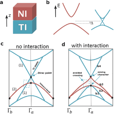
Herein, we construct a simple model to describe the interaction of the topological interface state with non-topological states at the interface. Although such situations may arise due to defects in the near interface region, they are a general consequence of misalignment of the band edges of the TI and the NI. Such misalignment leads to a large transverse -field in the vicinity of the interface which can localize bulk semiconductor bands to the near interfacial region – resulting in substantial interaction with the topological state. In this model, the pristine topological insulator states at the interface are described by a massless Dirac cone with helical (spin-momentum-locked) spin textures represented by the effective surface Hamiltonian, . Given that in general TIs have a narrow bulk bandgap, the simplest model would be to consider that the Dirac cone interacts with only a single band of the semiconductor, as shown in Fig. 1(b-c), which is described by a spin-degenerated parabola, . Using the basis , where are the topological insulators spinors and are the semiconductor spinors, we can write the interaction between the topological and semiconductor states in -space as follows,
| (1) |
where is the Fermi velocity associated with the topological surface state, is the effective mass of electrons(holes) in the semiconductor, and is the CBM(VBM) energy relative to Dirac point, as shown in Fig. 1(b). For the most general type of interaction, the interaction matrix can be expanded in terms of Pauli matrices,
| (2) |
where each is an independent complex parameter. In the absence of interaction, the solutions to equation (1) at the -point leads to two sets of doubly degenerate solutions; those associated with the Dirac-point of the topological interface state at and those of the doubly degenerate semiconductor state at . This degeneracy at the -point is the spin degeneracy which is guaranteed by Kramers theorem, whereby operating on the eigenfunction with the time reversal operator (where represents complex conjugation) yields the eigenfunction of the energy degenerate Kramers pair. It is the TRS which is said to protect the topological state, as only perturbations which break TRS (such as the presence of magnetic impurities) can break the degeneracy.
Herein, however, we focus our attention on perturbations which preserve the TRS, as these are most relevant at the “standard” TI/NI interface in the absence of localized magnetic moments or long range ordering. This is accomplished by requiring that commutes with the time reversal operator, at the time reversely invariant momenta (TRIM) points in the Brillouin zone (BZ). This leads to the following constraints for the -parameters:
| (3) |
whereby must be wholly real and , and are purely imaginary. Solving for the energy eigenvalues of equation (1) we find that indeed interactions of this form preserve the double degeneracy at the -point, with eigenvalues at
| (4) |
where we have defined the total magnitude of the interaction, . Upon first glance, not much seems to have changed, with the interaction increasing the energy between the Dirac point and the band edge from to . However, the interaction also leads to an avoided crossing off , as shown schematically in Fig. 1(d). While this interaction cannot in principle open a gap, as it is an avoided crossing between the doubly degenerate semiconductor band and the non-degenerate TI state, it necessarily leads to a region where the interaction causes the interconversion of the character of the semiconductor bands and the TI state. Note that the lower branches of the Dirac cone cannot directly join with the upper branch near the Dirac point as they cannot cross the semiconductor band and hence the lower branch of the TI state becomes degenerate with the bulk derived state at . As the degenerate states at become close in energy, neither of these degenerate states can be clearly distinguished as the Dirac-point as both exhibit the evolution of topological states into bulk semiconductor derived states.
In order to investigate the nature of these mixed states, particularly how the helical nature of the topological interface state is altered under the interaction, we investigate the spin-textures of the four bands of the model. In the current basis, the spin-textures of the Bloch eigenstates of the effective Hamiltonian are calculated by the expectation values of the matrices:
| (5) |
While as suggested by equation 4, the calculated band structure depends only on the total magnitude of the interaction, , the nature of the resulting spin-texture is found to be dependent on the details of the interaction and the relative magnitudes of the contributing ’s. Spin textures for the four bands for different choices for the non-vanishing interaction parameter are shown in Fig. 2.
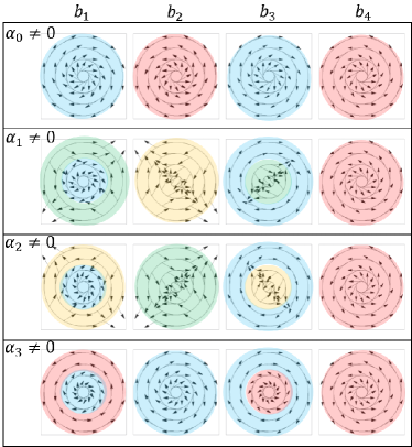
There are several novel features for these spin textures. Firstly, for all cases, all four bands in the model become spin-textured as a result of the interaction. In addition to the helical spin states associated with the TI interface state, interactions containing or terms can induce an anti-helical spin texturing in the bulk derived band. For these anti-helical states, see for instance the yellow shaded under , as you transverse the BZ in a counterclockwise direction the spin rotates in a clockwise manner, leading to a winding number of -1. Also interesting is the qualitative change in spin texture for individual bands, for instance under which changes from right-handed helical to left-handed helical at some critical . Although strange at first sight, this has a straightforward explanation – it corresponds to a change of character of the bands in the vicinity of an avoided crossing. Note that if the bulk derived state has a large curvature, it is possible for it to intersect with the Dirac cone twice instead of only once, leading to three distinct regions of spin texture. Although this second critical is not guaranteed to exist, we mention it here for the sake of completeness.
Focusing on the behavior close to , we see that the highest energy band, , keeps its left-handed helical nature under all interactions. This is expected as the semiconductor band intersects with the Dirac cone below the Dirac point, hence the spin texture of the top half of the Dirac cone () remains unchanged. Note however, that which one might expect to be associated with the bottom half of the Dirac cone (given that it is degenerate with at ) does possess the right-handed helical spin texture associated with the bottom half of the Dirac cone, but instead can be either left- or right- helical or anti-helical. Instead, it is found that only has the required right-handed helicity.
spin texture associated with the bottom half of the Dirac cone, irrespective of the interaction. This can be understood by referring back to schematic Fig. 1. Here the Dirac cone is split, with the bottom and top half of the Dirac cone no longer being degenerate at , but instead they become degenerate with the bulk derived semiconductor state, still satisfying the required degeneracy due to TRS. In order to find a system which may exhibit the exotic physical properties of the model, we turn to the technologically relevant Bi2Se3/GaAs interface.
In order to construct a realistic atomistic model of the Bi2Se3/GaAs interface, we use First-principles density functional theory calculations (see Methods) to first investigate the chemical stability and electronic properties of the isolated Se-treated As-terminated GaAs surface. In the unit cell, we considered Se replacing between 0 to 4 surface As, yielding to monolayer (ML) of Se coverage: , ML, ML, ML, and ML. Ball-and-stick models of geometries of GaAs surfaces with a Se-treatment of ML is shown in Fig. 3(a). The chemical stability map for the different Se coverages as a function of the chemical potentials and are shown in Fig. 3 (b). We focus our attention on the 0.75 ML coverage case as this is the most energetically stable surface for a large range of chemical potentials and leads to a fully passivated GaAs(111) surface which maintains its bulk band gap.
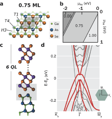
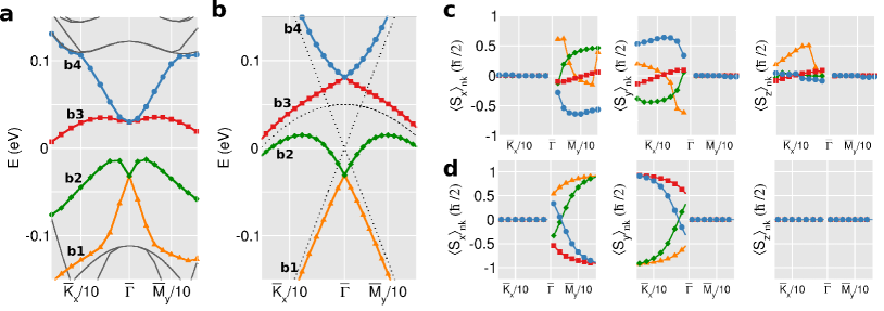
The interface is constructed by stacking QL of Bi2Se3 on the fully passivated 0.75ML Se substituted GaAs (111) surface, as shown in 3(c), with the Se atomic layer of Bi2Se3 directly above the substrate site indicated in Fig. 3 (a).The calculated band structure of the Bi2Se3/GaAs interface is shown in Fig. 3(d). In order to identify which states are localized at the interface and originate from the non-trivial band topology, we perform a local real space projection of each of the eigenfunctions onto the interfacial region shaded in Fig. 3 (c). The four bands which are most strongly localized to the interfacial region are shown highlighted in red in the bandstructure. An enlargement of the band structure near the -point and the accompanying spin textures of these four bands, labeled , are shown in Fig. 4(a) and (c), respectively. These four bands are directly comparable with the bands of the model, with and originating from the VBM of GaAs and becoming degenerate away from . Furthermore, the spin texture indicates appreciable spin-locking in the , , and bands.
To determine how representative the model presented in equation (1) is of the physics at the interface, we independently determine the material parameters for the model from first-principles calculation. We find a Fermi velocity of m/s for the Dirac cone of the pristine Bi2Se3, an effective mass of for the heavy-holes of the GaAs surface, and the relative VBM energy for the Bi2Se3/GaAs interface from workfunction calculations of eV. Using these parameters, we fit the single parameter associated with the interaction eV to produce the model bandstructure shown in Fig. 4 (b) to compare with the ab-initio bandstructure in Fig. 4 (a). By analyzing the spin textures of the first-principles calculations, we find that qualitative agreement can be reached when interaction is of the form , and hence we set and eV.
The spin texture of the model Hamiltonian is shown in Fig. 4 (d). The agreement of the features of band and compare quite well between the calculation and model, being primarily right and left-handed helical states, respectively, with the spin-momentum-locking of both greatly diminished in the immediate vicinity of . Bands and , however, appear less well described. While the nearly quenched spin-momentum-locking of from ab-initio calculation suggests that this band is less localized at the interface (and consequentially has less coupling), the origin of the deviation of from the model is clear. As we move away from the resulting decrease in the magnitude of spin is concurrent with the interaction of with lower lying bands which are not considered in the model. The spin-locking once again becomes more pronounced as the energy separation with lower lying bands increases. This suggests that including more bands in the model will lead to a more quantitatively accurate description. Nonetheless, we note that the essential feature of the model is also found in the DFT calculation. That being that the top-half of the Dirac cone, associated with left-handed helicity, and the bottom half of the Dirac-cone, associated with right-handed helicity, are separated by an energy gap at .
The model presented in eqn. (1) and the finding of its applicability to realistic interfaces suggest that not only is the particle-hole symmetry of the Dirac cone fundamentally broken at the interface, but that a number of new emerging phenomenon with potential applications exist. Firstly, while optical excitations from linearly polarized light are spin forbidden for an ordinary Dirac cone, the spin interaction present at the interfacial Dirac cone relaxes this selection rule, leading to a number of allowed transitions which generally become -dependent. This opens up the possibility of directly probing the topological interface states through optical means, such as absorption or photoluminescence. Furthermore, the well delineated regions of different spin texture shown in Fig. 2 indicate the presence of a -bottleneck. As electron relaxation into regions with a different spin texture would require a magnetic interaction, electron relaxation is now confined to individual shells of different spin textures with a prolonged excitation lifetime. In this way, it is similar to the phonon bottleneck which limits the relaxation rates of hot carriers in graphene fwang2014nanolett , potentially leading to photosensitive conductivity and the prospect of the formation of an excitonic condensate at the interface.
In summary, we present a general and simple model to describe the interaction of the interfacial Dirac-cone with non-topological states at the interface. The main features of the model are demonstrated in our parameter-free density-functional theory calculations of the Bi2Se3(0001)/GaAs interface. This interaction is found to lead to a number of emerging phenomenon which highlight the differences between the Dirac cone at the surface of a TI and that found at the interface. These includes the splitting of the Dirac cone (without breaking TRS), the acquisition of spin-texture of bulk derived bands, alteration of optical selection rules, the fundamental breaking of particle-hole symmetry, and the presence of a spin-bottleneck with associated long excitation lifetimes. While we have focused on the interaction of the emerging Dirac cone with bulk derived states at the TI/NI interface, the model is more general and could be trivially extended to investigate the interactions of the surface Dirac-cone with other non-topological states. These findings both suggest new possible phenomenon at the interface and may help to guide developments in TI/NI-based spintronics devices, especially due to the helical topological states role in spin current generationpesin2012spintronics ; li2014electrical and spin relaxationzutic2004spintronics .
Methods
The atomistic first principles calculations were performed within the Density Functional Theory (DFT) frameworkPhysRev.136.B864 ; PhysRev.140.A1133 as implemented in the Vienna Ab Initio Simulation Package (Vasp)PhysRevB.54.11169 ; PhysRevB.59.1758 . Energy cutoff of 300 eV and -points grid of in Monkhorst–Pack algorithmPhysRevB.13.5188 were taken as default on our calculations. The external potential was calculated using Projector Augmented-Wave (PAW) methodPhysRevB.50.17953 ; PhysRevB.59.1758 . The exchange-correlation functional was in Local Density Approximation (LDA)PhysRevLett.45.566 parameterized by Perdew–ZungerPhysRevB.23.5048 due to agreement with experimental bond lengths among Bi2Se3 quintuple-layersseixas2013topological . Electronic band structures and spin textures required non-collinear spin polarizations for spin-orbit interactions. The chemical stability of Se on the isolated As terminated GaAs(111) surface was determined by slab calculations in a 2x2 unit cell with 18 atomic layers. The Ga-terminated surface was passivated with H with a fractional charge (q=1.25 e). In order to minimize the effect of strain, a lattice constant of 4.07 was used in the interface calculation. The stacking with the Se atomic layer of Bi2Se3 directly above the substrate was chosen as it was found to be 20 and 490 meV/supercell lower in energy than the and configurations, respectively.
Authors contributions
L.S. performed the first principles calculations. L.S. and D.W performed effective Hamiltonian model calculations and wrote the manuscript with contributions from all authors. A.F. supervised the effort in Brazil and S.B.Z. conceived the project. All authors equally discussed the results and contributed to the understanding.
Acknowledgments
L.S. and A.F. acknowledges the financial support by the Brazilian agencies CNPq/INCT and FAPESP. L.S. also acknowledges partial financial support provided by Rensselaer Polytechnic Institute. D.W. acknowledges support from the Defense Award Research Project Agency, Award No. N66001-12-1-4304, and S.B.Z. acknowledges support from the US Department of Energy under Grant No. DE-SC0002623. Supercomputer time was provided by NERSC under Grant No. DE-AC02-05CH11231 and the Center for Computational Innovations at Rensselaer Polytechnic Institute.
References
- (1) Kane, C. L. & Mele, E. J. Quantum spin hall effect in graphene. Phys. Rev. Lett. 95, 226801 (2005).
- (2) Kane, C. L. & Mele, E. J. topological order and the quantum spin hall effect. Phys. Rev. Lett. 95, 146802 (2005).
- (3) Bernevig, B. A., Hughes, T. L. & Zhang, S.-C. Quantum spin hall effect and topological phase transition in hgte quantum wells. Science 314, 1757–1761 (2006).
- (4) Hasan, M. Z. & Kane, C. L. Colloquium: topological insulators. Rev. Mod. Phys. 82, 3045 (2010).
- (5) Qi, X.-L. & Zhang, S.-C. Topological insulators and superconductors. Rev. Mod. Phys. 83, 1057 (2011).
- (6) Chen, Y. L. et al. Experimental realization of a three-dimensional topological insulator, . Science 325, 178–181 (2009).
- (7) Hsieh, D. et al. A tunable topological insulator in the spin helical dirac transport regime. Nature 460, 1101–1105 (2009).
- (8) Alpichshev, Z. et al. STM imaging of electronic waves on the surface of Bi2Te3: topologically protected surface states and hexagonal warping effects. Phys. Rev. Lett. 104, 016401 (2010).
- (9) Koumoulis, D. et al. Nmr probe of metallic states in nanoscale topological insulators. Phys. Rev. Lett. 110, 026602 (2013).
- (10) Hsieh, D. et al. Observation of unconventional quantum spin textures in topological insulators. Science 323, 919–922 (2009).
- (11) Li, C. et al. Electrical detection of charge-current-induced spin polarization due to spin-momentum locking in bi2se3. Nature Nanotechnology 9, 218–224 (2014).
- (12) Fan, Y. et al. Magnetization switching throught giant spin-orbit torque in a magnetically doped topological insulator heterostructure. Nature Materials 13, 699–704 (2014).
- (13) Awschalom, D. & Samarth, N. Spintronics without magnetism. Physics 2, 50 (2009).
- (14) Shi, S.-F. et al. Controlling Graphene Ultrafast Hot Carrier Response from Metal-like to Semiconductor-like by Electrostatic Gating NanoLetters 14, 1578–1582 (2014).
- (15) Pesin, D. & MacDonald, A. H. Spintronics and pseudospintronics in graphene and topological insulators. Nature Materials 11, 409–416 (2012).
- (16) Žutić, I., Fabian, J. & Sarma, S. D. Spintronics: Fundamentals and applications. Rev. Mod. Phys. 76, 323 (2004).
- (17) Yoshimi, R. et al. Dirac electron states formed at the heterointerface between a topological insulator and a conventional semiconductor. Nature Materials 13, 253–257 (2014).
- (18) Hohenberg, P. & Kohn, W. Inhomogeneous electron gas. Phys. Rev. 136, B864–B871 (1964).
- (19) Kohn, W. & Sham, L. J. Self-consistent equations including exchange and correlation effects. Phys. Rev. 140, A1133–A1138 (1965).
- (20) Kresse, G. & Furthmüller, J. Efficient iterative schemes for ab initio total-energy calculations using a plane-wave basis set. Phys. Rev. B 54, 11169–11186 (1996).
- (21) Kresse, G. & Joubert, D. From ultrasoft pseudopotentials to the projector augmented-wave method. Phys. Rev. B 59, 1758–1775 (1999).
- (22) Monkhorst, H. J. & Pack, J. D. Special points for brillouin-zone integrations. Phys. Rev. B 13, 5188–5192 (1976).
- (23) Blöchl, P. E. Projector augmented-wave method. Phys. Rev. B 50, 17953–17979 (1994).
- (24) Ceperley, D. M. & Alder, B. J. Ground state of the electron gas by a stochastic method. Phys. Rev. Lett. 45, 566–569 (1980).
- (25) Perdew, J. P. & Zunger, A. Self-interaction correction to density-functional approximations for many-electron systems. Phys. Rev. B 23, 5048–5079 (1981).
- (26) Seixas, L., Abdalla, L., Schmidt, T., Fazzio, A. & Miwa, R. Topological states ruled by stacking faults in bi2se3 and bi2te3. J. Appl. Phys. 113, 023705–023705 (2013).