Magnetic imaging with an ensemble of Nitrogen Vacancy centers in diamond.
Résumé
The nitrogen-vacancy (NV) color center in diamond is an atom-like system in the solid-state which specific spin properties can be efficiently used as a sensitive magnetic sensor. An external magnetic field induces Zeeman shifts of the NV center levels which can be measured using Optically Detected Magnetic Resonance (ODMR). In this work, we quantitatively map the vectorial structure of the magnetic field produced by a sample close to the surface of a CVD diamond hosting a thin layer of NV centers. The magnetic field reconstruction is based on a maximum-likelihood technique which exploits the response of the four intrinsic orientations of the NV center inside the diamond lattice. The sensitivity associated to a area of the doped layer, equivalent to a sensor consisting of approximately NV centers, is of the order of . The spatial resolution of the imaging device is , limited by the numerical aperture of the optical microscope which is used to collect the photoluminescence of the NV layer. The effectiveness of the method is illustrated by the accurate reconstruction of the magnetic field created by a DC current inside a copper wire deposited on the diamond sample.
I Introduction
Measuring a magnetic field is a generic tool to investigate physical effects involving charge or spin displacement that appear in various fields such as spintronics, nanoelectronics, life-science Budker2007 . Examples are spin currents in graphene or carbone nanotubes, current propagation in nanoelectronics circuits, neuronal activity inducing a displacement of the action potential. In addition to sensitivity and spatial resolution, measuring not only the field intensity but also the full vectorial components is particularly valuable, as well as the ability to produce a full image of the sample.
During the past few decades a wealth of methods has been developed to sense and image magnetic fields. Various detection techniques have been investigated such as superconducting quantum interference devices (SQUID) McDermott25052004 , magnetic resonance force microscopy (MRFM) Rugar2004 ; Degen03022009 , alkali vapour atomic magnetometers Ledbetter19022008 ; Xu22082006 , and Bose-Einstein condensates PhysRevLett.98.200801 .
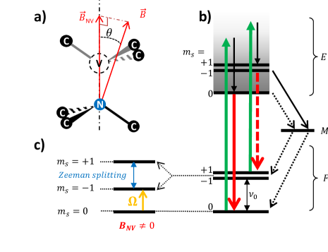
A particularly attractive technique is to develop magnetometers based on Nitrogen Vacancy centers (NV) in ultrapure diamond Rondin2014_0034-4885-77-5-056503 ; Schirhagl2014_doi:10.1146/annurev-physchem-040513-103659 . The NV center is a point defect consisting of a substitutional nitrogen atom (N) associated with a vacancy (V) located in an adjacent site of the diamond lattice (Fig. 1 a). It is as a perfectly photostable color center that emits a red fluorescence signal () when pumped with green light (). It is an atom-like system with well defined spin properties. It can be optically polarized and the fluorescence signal used to detect the spin transition induced by a microwave radiation, thus leading to Optically Detected Magnetic Resonance (ODMR) Gruber1997 .
NV centers can be produced as single defects with well controlled position within the diamond crystal through ion implantation Pezzagna2011 . In particular, the depth of the NV centers with respect to the surface can be controlled with a precision of a few nanometers. Thus NV centers can be used to realize solid-state, room temperature, optically addressed magnetic sensors Taylor2008 .
Two main kinds of NV based magnetometers have been developed up to now. Scanning probe magnetometers make use of a monolithic all-diamond scanning probe tip containing a single NV centre within from its end Maletinsky2012 . Sensitivity of and spatial resolution of can be obtained Grinolds2013 . An alternative solution consists in fixing a nanodiamond containing a single NV at the end of an Atomic Force Microscope tip Rondin2012 . Such technique has been used recently to visualize domain walls displacement between ferroelectric domains Tetienne20062014 .
The alternative solution is to use a high-density ensemble of NV centres, which should result in a signal to noise enhancement in with respect to a single center. Several devices exploiting that property have been demonstrated Steinert2010 ; Pham2011 ; LeSage2013 . They make use of an active layer of NV centers located close to the surface of a bulk diamond plate. The magnetic object is located close to this surface, and the magnetic field modifies the luminescence emitted by the NV centers. A microscope objective forms a diffraction limited image of the luminescence on a camera. This gives rise to a complete data acquisition over the whole object in one shot.
The goal of the present paper is to describe such a magnetic imaging set-up as well as the reconstruction method of the full vectorial magnetic field. We first recall the main properties of Nitrogen-Vacancy centers, and in particular those which are specific to ensembles. In a second part, we describe our experimental set-up, which, in particular, involves the total internal reflexion of the pump beam on the faces of the diamond sample. In a third part we describe how the projections of the field on the crystallographic axes can be obtained from the fluorescence images. In a fourth part, we detail the maximum-likelihood method that allows for the reconstruction of the magnetic field in each point of the measured image. Finally we study the sensitivity of our set-up and show how it can be optimized using differential acquisition.
II Magnetometry with ensemble of NV Centers
NV centers can exhibit different charge states. The negatively charged NV center (NV-) is a two electrons system with well defined energy levels associated with the spin state (Fig. 1 b). An essential feature of the NV- defect is that its ground level is a spin triplet , which degeneracy is lifted into a singlet state and a doublet state , separated by in the absence of magnetic field (zero-field splitting) Manson2006 . The single NV- center can be polarized in the state by optical pumping and the spin state detected by Optically Detected Magnetic Resonance (ODMR) (see Fig. 1 b).
When an external magnetic field is applied, the levels corresponding to and are shifted due to Zeeman effect and their resonance frequencies denoted et are shifted accordingly (Fig. 1 c). For magnetic fields lower than a few tens of Gauss Tetienne2012 , the Zeeman shift is linear and the positions of the lines are given by:
| (1) |
where is the zero field splitting of the ground state, is the electron spin gyromagnetic ratio and is the projection of the magnetic field along the (N-V) axis (Fig. 1 a). The frequency difference between the two lines scales linearly with , with the factor:
| (2) |
The NV center has symmetry. Its symmetry axis can take one of the four crystallographic directions of diamond, which results in four different projections of the magnetic field. Therefore, the OMDR spectrum of an ensemble of NV- centers exhibits four pairs of lines Steinert2010 ; Pham2011 . This feature is specific to NV ensembles as compared to single NV and, as detailed in the following, it can be exploited for vectorial reconstruction of the applied magnetic field.
Another point specific to ensembles concerns the sensitivity. When the number of collected photons is high, the signal is shot-noise limited and affected by Poisson noise. Thus the signal to noise ratio varies as and can be improved increasing the number of collected photons. This can be done two ways: first, increasing the number of ODMR spectra that are acquired sequentially and second, increasing the number of pixels and thus the corresponding integration area on the NV center active layer. The number of photons is thus proportional to the product of the integration area and the integration time . Therefore, the minimum detectable magnetic field is of the form:
| (3) |
where is the sensitivity of the set-up that can be derived measuring for various values of and . In our system is referred to an integration time of and an integration area of , and is thus given in .
III Experimental set-up
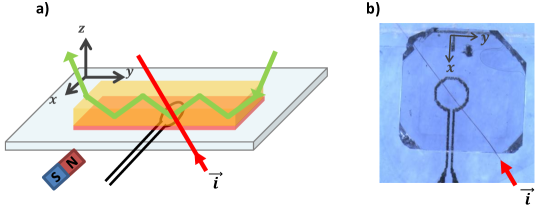
The central element of the sensor is the diamond plate holding a thin layer of NV centers implanted close to the surface, represented on Fig. 2. It is a oriented plate whose edges coincide with axes [100], [010] and [001] and define the laboratory frame denoted (x,y,z) (see Fig. 2). It is obtained from a oriented diamond sample grown by plasma assisted Chemical Vapour Deposition (CVD) Tallaire2006 on an High Pressure High Temperature (HPHT) substrate. The ultra-pure, single crystal, thick sample is then cut to produce a , thick plate. This thickness is chosen to allow the collection of the luminescence of the NV layer located on the back face through the diamond plate, taking into account the working distance of the microscope objective. This makes possible the study of opaque magnetic samples positioned underneath the plate (Fig. 2). Moreover, this thickness ensures good mechanical stability thus allowing optical quality polishing of the two main faces, which results in good imaging quality Almax . In addition, the four lateral faces are also optically polished to allow side pumping as detailed in the following.
In order to produce the suitable NV- layer, the diamond is uniformly implanted Pezzagna2010 with ions at the density of , at the limit of diamond graphitization Meijer2005_:/content/aip/journal/apl/87/26/10.1063/1.2103389 ; Prawer200093 . This concentration allows a high density of NV centres while avoiding luminescence quenching by neighboring Nitrogen atoms. The implantation energy is , which results in a layer located at about below the surface. The sample is then annealed at 800 C under vacuum for 2 hours to induce vacancy diffusion leading to the conversion of the implanted nitrogen atoms into luminescent NV color centers. With this energy, around of the ions are converted in NV- centres Pezzagna2010 , which results in a surface concentration around . Several characterizations performed on different tests samples have shown yield values around for similar implantation conditions Pezzagna2010 .
In our set-up, the pump laser is a Coherent - Verdi V5 producing a power beam at . Two configurations have been considered in order to optically pump the NV- layer. The first one, not represented here, consists in focusing the pump beam in the image principal plane of the microscope objective Steinert2010 ; Pham2011 in order to obtain a collimated beam on the object side. However, after having pumped the NV- layer, the beam can heat the sample and may damage it depending on its power. We have implemented an alternative solution LeSage2013 , represented in Fig. 2 a, that consists in propagating the pump beam into the diamond sample thanks to total internal reflections on the main faces, taking benefit of the high index of diamond . This technique is made possible thanks to optical quality polishing of the diamond plate side faces. The pump beam is incident on one side face of the diamond plate, and then experiences zigzag propagation, through total internal reflection, until it reaches the active layer located in the field of view of the microscope objective. Doing this, fragile samples can be studied even with a high power pump beam.
The photoluminescence from the NV- layer is collected with an immersion microscope objective having a high numerical aperture (N.A = 1.35). This results in a collection efficiency and a diffraction limited resolution of . The magnification of the microscope can be chosen by proper selection of its focusing lens. The NV- layer is imaged on the focal plane of an IDS camera with E2V CMOS sensor. The main characteristics of the imaging system such as pixel size of the camera, typical magnification value and the corresponding pixel sizes on the sample are given in Table 1.
For a typical exposure time of a pixel returns a signal close to saturation associated with a signal to noise ratio close to . Those measured values are consistent with the ones estimated from the sensitivity of the camera. In addition, we have measured that the signal to noise evolves as , which confirms that our measurement is shot-noise limited.
Finally, a ring shape antenna formed by a short-circuit at the end of a coaxial cable powered by a frequency tunable microwave synthesizer provides an oscillating microwave magnetic field that is used to induce the magnetic resonances of the NV centres.
| Parameter | symbol | value |
|---|---|---|
| Pumping wavelength | ||
| Pumping power | ||
| Exposure time | ||
| Size of the CMOS array pixels | ||
| Microscope magnification | ||
| Pixel size on the active layer | ||
| Signal to noise ratio (one pixel) | ||
| Contrast of ODMR lines | ||
| Linewidth (at half maximum) |
IV Data acquisition and treatment
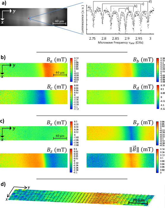
The set-up described above allows to perform an image of the NV- layer, and for each pixel, to retrieve the ODMR spectrum. The frequency of the microwave synthesizer is swept around the central frequency . For each frequency step, a complete luminescence image is taken (Fig. 3 a). The images are appended in the computer memory to form a 3D volume of data giving the value of the luminescence for each pixel (x,y) of the camera and for each frequency () of the sweep. This volume of data can also be considered as an image in which each (x,y) pixel returns a full ODMR spectrum. Fig. 3 a presents such a spectrum taken from a pixel at the centre of the image. A static magnetic field is applied to shift the lines away from degeneracy. The spectrum exhibits four pairs of lines, denoted , , and corresponding to the four possible orientations of the NV- centre. Each pair corresponds to the frequencies and located symmetrically each side of the central frequency . The distance between the two peaks in one pair is directly related to the projection of the applied magnetic field on the corresponding N-V axis (Eq. 2).
The precise position of the eight resonances are determined for each pixel using the Levenberg-Marquardt algorithm Levenberg1944 ; Marquardt1963 to fit the following multi-Lorentzian, multi-parameter function on the data:
| (4) |
where is the Lorentzian function, is the contrast of the line’s pair , is the central position of the pair, is the Zeeman distance between the two lines of the pair and is their linewidth.
The algorithm requires inputs for the fitting parameters that are not too far from the result. So, a pre-selection of those parameters is performed manually for a pixel in the centre of the image. Then the entire image is fitted gradually taking the results of the neighboring already fitted pixels as an input for the following one.
At the end , , and , the distance between the two transition for each class of NV centre, are obtained for each pixel of the camera. As a convention, , , and are chosen in the following order:
| (5) |
The measurements of the magnetic field projected on the four possible NV orientations are denoted , , and . Their absolute values are derived using Eq. (2) and Eq. (5). The sign of those projections and the orientation of the axes , , and with respect to the laboratory frame are then to be determined.
, , and are the unit vectors representing the four possible orientations of the NV axes. Due to the symmetry properties of the NV centres, they are related by:
| (6) |
Taking the projection of this equation along the field gives:
| (7) |
Both field and have the same signature on the NV centres and cannot be distinguished with our system. We choose . Then , verifying both Eq. (5) and Eq. (7) have necessarily a sign opposite to that of . In the absence of noise, should be directly deduced from Eq. (7). In the presence of noise, we choose the sign of , minimizing the relation . With this method, we can most probably find the good values of the field projections from the measured .
In practice, the fitting algorithm is robust. It returns a reliable value if the contrast exceeds approximatively twice the noise fluctuations i.e. when the ODMR line is hardly visible from the noise. Considering a typical contrast of and a signal to noise ratio for a single sweep close to (Table 1) an average of only four sweeps is sufficient to successfully retrieve the experimental parameters. The fitting algorithm works with a minimum of or frequency samples within an ODMR line. So considering a typical linewidth of , a sampling resolution of is sufficient. As a result, for a typical frequency span of , 150 frequency samples (i.e. images) are necessary. Considering a minimum number of 4 sweeps and an exposure time of 2.5 ms, the minimum duration for the entire measurement is around for a spatial sampling of one pixel on the camera, corresponding to on the diamond plate. Instead of accumulating several frequency sweeps, the signal to noise ratio can be increased by spatial binning of the camera pixels. A binning of , corresponding to a spatial resolution on the diamond plate, requires only one frequency sweep and an acquisition time around to result in a signal to noise ratio equivalent to the one obtained in the previous case. Therefore, an optimization of the spatial resolution / acquisition time can be performed.
V Magnetic field reconstruction
Once the projections of the magnetic field on the crystallographic axes have been determined, the following step is to reconstruct the magnetic field in the laboratory frame. The measured field components do not directly give the magnetic field , but are affected by some noise inherent to the measurement. To account for that effect, we retrieve the best evaluation of the magnetic field knowing the values of using a maximum-likelihood method.
We define the frame in which , , and have the following coordinates:
| (8) |
Due to the (100) orientation of the diamond, each axis , and coincides with the edges of the plate (Fig. 2 a). However, they are still to be attributed to each axis , and of the laboratory frame since the orientations of the crystalline axes , , and are chosen with respect to (cf. Eq. 5), which can have an arbitrary direction.
We consider a Gaussian noise distribution with standard deviation . The probability to measure along axis knowing and thus is given by:
| (9) |
Thus, the probability to measure , , and knowing is:
| (10) |
with given by
| (11) |
According to Bayes theorem, we can interpret Eq. (10) as the likelihood to have a magnetic field equal to , knowing the actual measurements , , and . Thus, the best estimation of would minimize .
Therefore, we express the projections of the magnetic field on the direction, , as functions of , and and substitute these expressions in . Then we minimize with respect to , and and obtain the expressions of the most likely magnetic field components as a function of , , and :
| (12) |
The advantage of those expressions is to involve the four measured projections of the field, , and, thus, to exploit all the available information. They give the best estimate of , even if the measurement is affected by noise.
The last step is to find the proper permutation of axes , , in order to retrieve the components of the magnetic field in the laboratory frame. This can be solved exploiting prior knowledge on the sample. Another possibility is to add an auxiliary known magnetic field (for example by adding a CW current in the antenna), that allows identifying the four lines , , and with respect to the laboratory frame.
As an example, Fig. 3 displays such a reconstruction for a magnetic field produced by a current of in a diameter copper wire. In this case the shape of the magnetic field distribution that is expected is known a priori which allows to attribute the good directions to the magnetic field components.
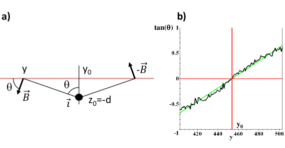
Once the magnetic field is known, it can be used to retrieve the characteristics of the source. In the case of a wire, this can be done by simple geometrics considerations. Up to small misalignments, the wire is aligned with axis. The circulating current produces an ortho-radial magnetic field located mainly in the plane. The lines perpendicular to the fields in each position along the NV center layer are characterized by the angle and intersect at the location of the wire . Knowing and , we express at each position :
| (13) |
A linear fit of the data intersects the line and gives the value of . The inverse of the slope gives the value of . As a consequence the wire can be positioned with respect to the NV center layer. Considering the field measurements on one side of the field we can extract the values and expressed in pixels units. Taking into account the effective size of the pixel on the NV layer (Table 1), we obtain = 95.3 m and d = 15.9 m. This value is consistent with the 20 m nominal diameter of the copper wire, also holding an additional isolating cover. The difference between the measured distance and the wire radius can be explained by the fact that the wire is not sticked to the diamond plate.
In addition, measuring the norm of the magnetic field allows to estimate the current circulating in the wire. For a position on the NV centers layer, the current is given by
| (14) |
Averaging the values obtained in the vicinity of the magnetic field maximum gives a result of 10.5 mA. Altough a little lower than the expected value (12 mA), this value shows that a good quantitative agreement can be obtained from our simple method.
We have performed the same evaluation on the other side of the field located at x = 37.4 m (178 pixels). We obtain a wire position given by = 16.0 m (76 pixels) and = 98.6 m (469 pixels). This shows that the wire is almost perfectly parallel to the NV layer and that there is a small tilt angle of 5 with respect to x axis. We have calculated a 10.2 mA current in the wire for that position, close to the one obtained on the other side of the sample. The slight difference is due to the simplifications in our method that considers two independent (y,z) planes. A more precise method should involve one uniform current in the wire all along the sample and exploit all available magnetic field measurements.
This simple reconstruction method shows that our technique is suited for retrieving the characteristics of simple objects such as a wire. It could be extended further to study the characteristics of more complicated source distributions.
VI Sensitivity
In the previous part, we have depicted a method allowing a vectorial reconstruction of the magnetic field starting from the measurement of the field projections on the crystallographic axes. Here, we evaluate the sensitivity of this technique and estimate the maximum sensitivity of our set-up according to our experimental parameters.
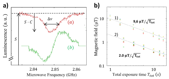
We first determine experimentally the efficiency of the fitting algorithm. Therefore, we measure two times the same uniform magnetic field consecutively. We then subtract the data and perform a statistics over a large number of pixels. The resulting variance is two times the variance of one measurement . The minimum detectable magnetic field , normalized to a 1 integration area, is given in Fig. 5 b as a function of the total acquisition time . We have limited our acquisition time to 10 s, which is indeed long with respect to many physical phenomena. Over this time-scale, the minimum detectable magnetic field features a shot-noise scaling. On the other hand, we investigated how the signal-to-noise ratio can be improved by increasing the integration surface. Starting from one pixel, we found that the signal-to-noise ratio has a shot-noise dependence until the integration surface reaches 8 x 8 pixels where it starts to saturate. For a pixel number around 1500, increasing further the number of integrated pixels does not bring any advantage anymore. This is probably due to the presence of technical noise in the camera response that induces correlated fluctuations between the pixels. Of course, this increase of signal-to-noise ratio by pixel integration is obtained at the price of spatial resolution.
From line in Fig. 5 b, we retrieve the normalized sensitivity of the fitting algorithm:
| (15) |
Then, we evaluate the maximal sensitivity that can be expected from our set-up. It is determined from an ODMR line such as the curve (a) of Fig. 5 a. The total luminescence signal is . The amplitude of the resonance is where is the contrast. The linewidth is . The maximum of the slope is obtained close to the line half-maximum and is equal to . The factor comes from the shape of the line that is assumed Lorentzian. The noise is the standard deviation of the monitored signal .
The sensitivity is calculated from the parameters values obtained for one pixel of the camera that are given in Table 1. We obtain Taylor2008 ; Maze2008 :
| (16) |
This value is better than the one obtained with the fitting algorithm given by Eq. (15). The ratio between those two values is given by , which shows that, over a complete spectrum given by , only the part corresponding to the two resonance lines necessary to retrieve the magnetic field, , actually brings useful information on that field.
In order to optimise the measurement time, all the acquisitions have to be taken in the frequency range where the slope of the line is maximum. Having a prior estimation of its position , we can acquire two images at frequencies and . The difference is immune from the common mode noise and proportional to the shift of the magnetic field with respect to the central position Schoenfeld_PhysRevLett.106.030802 ; Rondin2012 . A normalisation by cancels the spatial variation of the pumping beam intensity. We can then calculate the error function
| (17) |
that is represented by the curve (b) of Fig. 5 a. Knowing the contrast and the linewidth, we can retrieve the minimum detectable magnetic field from the measured signal as a function of the total acquisition time . It is fitted by the line in Fig. 5 b. The resulting sensitivity is
| (18) |
which matches exactly the value of . Therefore this differential method allows to obtain the maximum sensitivity of our set-up once the line positions have been determined by the fitting algorithm. Another advantage of this differential method is that the measurement of the slope requires only two frequency measurements and thus two images, leading to much shorter acquisition times.
The contrast and the resonance linewidth are essential parameters determining the sensitivity. We have measured contrasts in the range of to . Those values are smaller than those obtained with single NV centers (typ. ). This difference can be explained from several origins. First, we collect at the same time the luminescence from 4 sets of NV centers corresponding to the 4 possible orientations. Only one set is resonant at a time, the three others result in a background signal that leads to a factor four decrease of the contrast value as compared to single NV centers. Second, our sample includes neutral NV centers (NV0) as well which contribute to the background luminescence. Third, the pumping intensity is necessarily much lower with ensemble, due to the fact that a large surface is to be pumped. Thus, the polarization in the state is lower. Finally, our sample is heavily doped with N ions. Thus each NV center is surrounded with a high density electron spin bath that can result in a short relaxation time and a decrease of the polarization rate. The combination of those various effects can explain the low contrast obtained with our set-up.
Several improvement directions can be foreseen. Preferential NV orientation can be obtained thanks to controlled N doping during the growth of diamond over specific orientations Lesik2014_:/content/aip/journal/apl/104/11/10.1063/1.4869103 ; Michl2014_:/content/aip/journal/apl/104/10/10.1063/1.4868128 ; Fukui2014_1882-0786-7-5-055201 . In addition, controlling the charge state with suited surface termination :/content/aip/journal/apl/96/12/10.1063/1.3364135 would allow to increase the rate of useful NV- centers as compared to NV0 centers.
The observed linewidth is in the range of 7 MHz. One possible explanation of this linewidth can come from the power broadening due to continuous pumping. Using pulsed measurement protocols Taylor2008 can avoid that effect and result in sharper lines as has been observed with single NV centers with linewidth in the range of 100 kHz Dreau2011 . Line broadening can also come from the electron spin bath resulting from the high quantity of Nitrogen atoms that are not converted into NV centers. Increasing the yield of the conversion from N to NV using techniques such as electron or proton irradiation would allow to work with a lower concentration of Nitrogen and thus decrease this effect. Ultimately, isotopically enriched diamond can eliminate the nuclear spin bath due to that are present in natural diamond.
VII Conclusion
In this work, we have exploited the ODMR signal of an ensemble of NV centers in order to quantitatively map the vectorial structure of a magnetic field produced by a sample close to the surface of a CVD diamond hosting a thin layer of NV centers. The reconstruction of the magnetic field is based on a maximum-likelihood technique which exploits the response of the four intrinsic orientations of the NV center inside the diamond lattice. The sensitivity associated to a area of the doped layer, equivalent to a sensor consisting of approximately NV centers, is of the order of . The spatial resolution of the imaging device is , limited by the numerical aperture of the optical microscope which is used to collect the photoluminescence of the NV layer. The effectiveness of this technique is illustrated by the accurate reconstruction of the magnetic field created by a DC current inside a copper wire deposited on the diamond plate. We have investigated the limitations that are either specific to our technique or related to the physical properties of our diamond crystal. We have proposed several improvement directions that should allow to reach sensitivities in the range for an integration area of .
VIII Acknowledgements
The research leading to these results has received funding from the European Union Seventh Framework Programme (FP7/2007-2013) under the project DIADEMS (grant agreement n∘ 611143) and from the Agence Nationale de la Recherche (ANR) under the project ADVICE (grant ANR-2011-BS04-021).
Références
- [1] Dmitry Budker and Michael Romalis. Optical magnetometry. Nat. Phys, 3(4):227–234, April 2007.
- [2] Robert McDermott, SeungKyun Lee, Bennie ten Haken, Andreas H. Trabesinger, Alexander Pines, and John Clarke. Microtesla mri with a superconducting quantum interference device. Proceedings of the National Academy of Sciences of the United States of America, 101(21):7857–7861, 2004.
- [3] D. Rugar, R. Budakian, H. J. Mamin, and B. W. Chui. Single spin detection by magnetic resonance force microscopy. Nature, 430(6997):329–332, July 2004.
- [4] C. L. Degen, M. Poggio, H. J. Mamin, C. T. Rettner, and D. Rugar. Nanoscale magnetic resonance imaging. Proceedings of the National Academy of Sciences, 106(5):1313–1317, 2009.
- [5] M. P. Ledbetter, I. M. Savukov, D. Budker, V. Shah, S. Knappe, J. Kitching, D. J. Michalak, S. Xu, and A. Pines. Zero-field remote detection of nmr with a microfabricated atomic magnetometer. Proceedings of the National Academy of Sciences, 105(7):2286–2290, 2008.
- [6] Shoujun Xu, Valeriy V. Yashchuk, Marcus H. Donaldson, Simon M. Rochester, Dmitry Budker, and Alexander Pines. Magnetic resonance imaging with an optical atomic magnetometer. Proceedings of the National Academy of Sciences, 103(34):12668–12671, 2006.
- [7] M. Vengalattore, J. M. Higbie, S. R. Leslie, J. Guzman, L. E. Sadler, and D. M. Stamper-Kurn. High-resolution magnetometry with a spinor bose-einstein condensate. Phys. Rev. Lett., 98:200801, May 2007.
- [8] L Rondin, J-P Tetienne, T Hingant, J-F Roch, P Maletinsky, and V Jacques. Magnetometry with nitrogen-vacancy defects in diamond. Reports on Progress in Physics, 77(5):056503, 2014.
- [9] Romana Schirhagl, Kevin Chang, Michael Loretz, and Christian L. Degen. Nitrogen-vacancy centers in diamond: Nanoscale sensors for physics and biology. Annual Review of Physical Chemistry, 65(1):83–105, 2014. PMID: 24274702.
- [10] A. Gruber, A. Dräbenstedt, C. Tietz, L. Fleury, J. Wrachtrup, and C. Von Borczyskowski. Scanning confocal optical microscopy and magnetic resonance on single defect centers. Science, 276(5321):2012–2014, June 1997.
- [11] Sébastien Pezzagna, Detlef Rogalla, Dominik Wildanger, Jan Meijer, and Alexander Zaitsev. Creation and nature of optical centres in diamond for single-photon emissionâoverview and critical remarks. New J. Phys., 13(3):035024, March 2011.
- [12] J. M. Taylor, P. Cappellaro, L. Childress, L. Jiang, D. Budker, P. R. Hemmer, A. Yacoby, R. Walsworth, and M. D. Lukin. High-sensitivity diamond magnetometer with nanoscale resolution. Nat. Phys, 4(10):810–816, September 2008.
- [13] P. Maletinsky, S. Hong, M. S. Grinolds, B. Hausmann, M. D. Lukin, R. L. Walsworth, M. Loncar, and A. Yacoby. A robust scanning diamond sensor for nanoscale imaging with single nitrogen-vacancy centres. Nat. Nano., 7(5):320–324, April 2012.
- [14] MS Grinolds, S Hong, P Maletinsky, L Luan, MD Lukin, RL Walsworth, and A Yacoby. Nanoscale magnetic imaging of a single electron spin under ambient conditions. Nature Physics, 9(4):215–219, 2013.
- [15] L. Rondin, J.-P. Tetienne, P. Spinicelli, C. Dal Savio, K. Karrai, G. Dantelle, A. Thiaville, S. Rohart, J.-F. Roch, and V. Jacques. Nanoscale magnetic field mapping with a single spin scanning probe magnetometer. Appl. Phys. Lett., 100(15):–, 2012.
- [16] J.-P. Tetienne, T. Hingant, J.-V. Kim, L. Herrera Diez, J.-P. Adam, K. Garcia, J.-F. Roch, S. Rohart, A. Thiaville, D. Ravelosona, and V. Jacques. Nanoscale imaging and control of domain-wall hopping with a nitrogen-vacancy center microscope. Science, 344(6190):1366–1369, 2014.
- [17] S. Steinert, F. Dolde, P. Neumann, A. Aird, B. Naydenov, G. Balasubramanian, F. Jelezko, and J. Wrachtrup. High sensitivity magnetic imaging using an array of spins in diamond. Rev. Sci. Instrum., 81(4):043705–043705–5, April 2010.
- [18] L M Pham, D Le Sage, P L Stanwix, T K Yeung, D Glenn, A Trifonov, P Cappellaro, P R Hemmer, M D Lukin, H Park, A Yacoby, and R L Walsworth. Magnetic field imaging with nitrogen-vacancy ensembles. New J. Phys., 13(4):045021, April 2011.
- [19] D Le Sage, K Arai, DR Glenn, SJ DeVience, LM Pham, L Rahn-Lee, MD Lukin, A Yacoby, A Komeili, and RL Walsworth. Optical magnetic imaging of living cells. Nature, 496(7446):486–489, 2013.
- [20] N. Manson, J. Harrison, and M. Sellars. Nitrogen-vacancy center in diamond: Model of the electronic structure and associated dynamics. Phys. Rev. B, 74(10), September 2006.
- [21] J-P Tetienne, L Rondin, P Spinicelli, M Chipaux, T Debuisschert, J-F Roch, and V Jacques. Magnetic-field-dependent photodynamics of single nv defects in diamond: an application to qualitative all-optical magnetic imaging. New Journal of Physics, 14(10):103033, 2012.
- [22] A. Tallaire, A.T. Collins, D. Charles, J. Achard, R. Sussmann, A. Gicquel, M.E. Newton, A.M. Edmonds, and R.J. Cruddace. Characterisation of high-quality thick single-crystal diamond grown by CVD with a low nitrogen addition. Diam. Rel. Mat., 15(10):1700–1707, October 2006.
- [23] Almax easyLab bvba. http://www.almax-easylab.com.
- [24] S Pezzagna, B Naydenov, F Jelezko, J Wrachtrup, and J Meijer. Creation efficiency of nitrogen-vacancy centres in diamond. New Journal of Physics, 12(6):065017, 2010.
- [25] J. Meijer, B. Burchard, M. Domhan, C. Wittmann, T. Gaebel, I. Popa, F. Jelezko, and J. Wrachtrup. Generation of single color centers by focused nitrogen implantation. Applied Physics Letters, 87(26):–, 2005.
- [26] S Prawer, K.W Nugent, D.N Jamieson, J.O Orwa, L.A Bursill, and J.L Peng. The raman spectrum of nanocrystalline diamond. Chemical Physics Letters, 332(1 2):93 – 97, 2000.
- [27] Kenneth Levenberg. A method for the solution of certain problems in least squares. Quarterly of applied mathematics, 2:164–168, 1944.
- [28] Donald W Marquardt. An algorithm for least-squares estimation of nonlinear parameters. Journal of the Society for Industrial & Applied Mathematics, 11(2):431–441, 1963.
- [29] J. R. Maze, P. L. Stanwix, J. S. Hodges, S. Hong, J. M. Taylor, P. Cappellaro, L. Jiang, M. V. Gurudev Dutt, E. Togan, A. S. Zibrov, A. Yacoby, R. L. Walsworth, and M. D. Lukin. Nanoscale magnetic sensing with an individual electronic spin in diamond. Nature, 455(7213):644–647, October 2008.
- [30] Rolf Simon Schoenfeld and Wolfgang Harneit. Real time magnetic field sensing and imaging using a single spin in diamond. Phys. Rev. Lett., 106:030802, Jan 2011.
- [31] M. Lesik, J.-P. Tetienne, A. Tallaire, J. Achard, V. Mille, A. Gicquel, J.-F. Roch, and V. Jacques. Perfect preferential orientation of nitrogen-vacancy defects in a synthetic diamond sample. Applied Physics Letters, 104(11):–, 2014.
- [32] Julia Michl, Tokuyuki Teraji, Sebastian Zaiser, Ingmar Jakobi, Gerald Waldherr, Florian Dolde, Philipp Neumann, Marcus W. Doherty, Neil B. Manson, Junichi Isoya, and J rg Wrachtrup. Perfect alignment and preferential orientation of nitrogen-vacancy centers during chemical vapor deposition diamond growth on (111) surfaces. Applied Physics Letters, 104(10):–, 2014.
- [33] Takahiro Fukui, Yuki Doi, Takehide Miyazaki, Yoshiyuki Miyamoto, Hiromitsu Kato, Tsubasa Matsumoto, Toshiharu Makino, Satoshi Yamasaki, Ryusuke Morimoto, Norio Tokuda, Mutsuko Hatano, Yuki Sakagawa, Hiroki Morishita, Toshiyuki Tashima, Shinji Miwa, Yoshishige Suzuki, and Norikazu Mizuochi. Perfect selective alignment of nitrogen-vacancy centers in diamond. Applied Physics Express, 7(5):055201, 2014.
- [34] K.-M. C. Fu, C. Santori, P. E. Barclay, and R. G. Beausoleil. Conversion of neutral nitrogen-vacancy centers to negatively charged nitrogen-vacancy centers through selective oxidation. Applied Physics Letters, 96(12):–, 2010.
- [35] A. Dréau, M. Lesik, L. Rondin, P. Spinicelli, O. Arcizet, J.-F. Roch, and V. Jacques. Avoiding power broadening in optically detected magnetic resonance of single NV defects for enhanced dc magnetic field sensitivity. Phys. Rev. B, 84(19):195204, November 2011.