Inelastic carrier lifetime in a coupled graphene / electron-phonon system: Role of plasmon-phonon coupling
Abstract
We calculate the inelastic scattering rates and the hot electron inelastic mean free paths for both monolayer and bilayer graphene on a polar substrate. We study the quasiparticle self-energy by taking into account both electron-electron and electron-surface-optical-phonon interactions. In this calculation the leading-order dynamic screening approximation (G0W approximation) is used to obtain the quasiparticle self-energy by treating electrons and phonons on an equal footing. We find that the strong coupling between the surface-optical phonon and the plasmon leads to an additional decay channel for the quasiparticle through the emission of the coupled mode, and gives rise to an abrupt increase in the scattering rate, which is absent in the uncoupled system. In monolayer graphene a single jump in the scattering rate occurs, arising from the emission of the low-energy branch of the coupled plasmon-phonon modes. In bilayer graphene the emission of both low- and high-energy branches of the coupled modes contributes to the scattering rate and gives rise to two abrupt changes in the scattering rate. The jumps in the scattering rate can potentially be used in hot electron devices such as switching devices and oscillators.
I Introduction
Two-dimensional (2D) graphene has been extensively studied during recent years because of its fundamental and technological interest. sarmarmp2011 ; netormp2009 Although it is possible to grow graphene on non-polar substrates,Wu2011 in most currently available graphene samples (e.g., graphene field-effect transistors) graphene lies on top of a polar substrate such as SiO2,chennatnano2008 ; Dorgan2010 ; Fei2011 SiC,Robinson2009 ; Sutter2009 ; Liu2010 ; Koch2010 hBNdean2010 ; wang2013 ; Ulstrup ; Principi or HfO2.Zou2010 In such graphene samples the polar optical phonons of the substrate are localized near the graphene-substrate interface, and free carriers in graphene couple to the surface polar (SO) phonons of the underlying substrate through the long-range polar Fröhlich coupling. In polar materials the longitudinal optical (LO) phonons generate a long-range electric field which scatters electrons, and typically their contribution to resistivity is dominant at room temperatures. andormp1982 In non-polar materials such as graphene, however, the non-polar optical phonons have little effect on carrier transport because the long-range interaction between electrons and phonons is absent and the energy of the (non-polar) optical phonon is very high, 200 meV. In addition, contributions from acoustic phononshwang2008 ; park2014 ; sohier2014 ; Zhang2014 are relatively small because the electron-acoustic-phonon coupling is rather weak in graphene due to the small deformation potential.min2011 ; efetov2010 ; Pachoud2010 ; dawlaty For this reason, the SO phonons rather than non-polar LO or acoustic phonons can be the dominant scattering source at room temperature in graphene on a polar substrate. chennatnano2008 ; Zou2010 ; Yan2013
In addition to being the main scattering source in transport, it is well known that in polar materials the electron-polar-optical-phonon interaction leads to polaronic many-body renormalization of the single particle properties, e.g., polaronic Fermi velocity (effective mass) renormalization and broadening of the quasiparticle spectral function.Mason1985 ; mahan ; Tse2007 ; LeBlanc2011 ; Carbotte2013 Even though these effects are expected to be small in graphene due to the weak Fröhlich coupling arising from the spatial separation between electrons in graphene and the surface of a substrate and due to the large dielectric constant of the substrate, there is a much stronger quantitative manifestation of electron-SO-phonon coupling in graphene on a polar substrate, which is the macroscopic coupling of the electronic collective modes (i.e., plasmons) to the SO phonons of the system via the long-range Fröhlich coupling. This mode coupling phenomenon, which hybridizes the collective plasmon modes of the electron gas with the SO-phonon modes of the substrate, gives rise to coupled plasmon-phonon modes, which have been extensively studied both experimentallyLiu2010 ; Zhu2014 ; Fei2011 ; Koch2010 ; Brar2014 and theoreticallyph_el ; Jablan2011 ; Ong2012 in graphene. The plasmon-phonon coupling is important in many single-particle properties including the inelastic carrier life time, hot-electron energy-loss processes, and transport properties.
The objective of this paper is to provide the inelastic carrier lifetime and the inelastic mean free path of monolayer and bilayer graphene in the presence of the long-range polar Fröhlich coupling between electrons in graphene and SO phonons in the underlying polar substrate within the leading-order perturbation theory, i.e., G0W approximation. We consider the effective total interaction (i.e., the coupled electron-electron and electron-SO-phonon interaction) within the framework of the random phase approximation (RPA). Even though the problem is treated within the G0W framework of the leading-order effective interaction approximation, our results should be quite valid in graphene because graphene has a very weak Fröhlich coupling, which justifies the neglect of the electron-phonon vertex corrections. We include, however, important physical effects of the dynamical screening, phonon self-energy correction, plasmon-phonon mode coupling, and Landau damping. In the presence of electron-SO-phonon coupling we find added features in the inelastic carrier lifetime, which are obviously absent without the coupling.
There have been several studies upon the effects of electron-SO-phonon interaction in graphene.SSC ; scharf2013 ; fratini2008 ; Schiefele2008 ; Li2008 Various many-body quantities such as- the self-energy, scattering rate, and spectral function have been calculated for the statically screened electron-SO- phonon interaction. Such calculations based on the static screening approximation are justified when the charge carrier density is high enough that the corresponding Fermi energy exceeds the SO phonon energy. However, the SO phonon energies of the common polar substrates for graphene such as SiC or SiO2 range from 50 to 200 meV, and they are comparable to the typical Fermi energies of graphene, 100 – 300 meV. Thus the dynamic screening of the electron-SO- phonon interaction is more desirable. Ong2012 In addition, because the SO phonon energy and the energy of electrons are comparable, we cannot treat the electron-electron interaction and the electron-SO phonon interaction separately. Therefore, we need to treat both interactions equivalently within the same dynamic screening approximation. Quasiparticle properties of various systems have been calculated considering both electron-electron and electron-phonon interactions.2DEG ; hwang1995 However, there appears to be a lack of calculation of quasiparticle properties of graphene on a polar substrate with both electron-electron and electron-SO-phonon interactions equally treated.
In this paper, we calculate the scattering rate (-1) and the corresponding inelastic mean free path () of quasiparticles in both monolayer and bilayer graphene by taking into account both electron-electron and electron-SO-phonon interactions. We also investigate the effect of the dynamic screening of the electron-SO-phonon interaction and plasmon-phonon coupling. In addition, we propose a possible technological application to a lateral hot-electron transistor by making use of the electron-SO- phonon interaction effect. Throughout the paper, we refer to the graphene system with both electron-electron and electron-SO-phonon interactions as the coupled system, whereas the graphene system with only the electron-electron interaction as the uncoupled system.
The paper is organized as follows. In Section II the generalized theory is presented for calculating the electron self-energy in the presence of both electron-electron and electron-SO phonon interactions. Section III presents the results for the scattering rates and the hot electron mean free paths for both monolayer and bilayer graphene. We summarize in Sec. IV with a discussion.
II Theory
We consider the two component effective Hamiltonian for both monolayer and bilayer graphene, which is given bymccann2006 ; mccann2007
| (1) |
where corresponds to monolayer (bilayer) graphene, is the nearest interlayer hopping, is the in-plane velocity of monolayer graphene, and . The corresponding energy eigenvalues and eigenfunctions are given by and where are band indices.
For monolayer graphene, this model holds over the Fermi energy range limited by intralayer coupling (3 eV) while for bilayer graphene it is valid for the Fermi energy range limited by the interlayer coupling (0.4 eV), which is still within the range we are considering in this work. Note that if the Fermi energy or the corresponding carrier density is high enough, the interlayer hopping can be negligible and the bilayer graphene is simply described by a collection of two monolayer graphene sheets. We will discuss the high carrier density limit in bilayer graphene later.
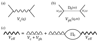
In the coupled system, electrons interact with each other through the direct Coulomb interaction [Fig. 1(a)] and the SO-phonon-mediated interaction [Fig. 1(b)]. Here the electron-SO phonon coupling is given bymahan
| (2) |
where is the distance between the graphene and the polar substrate,
| (3) |
() is the zero- (high) frequency dielectric constant, and is the bare SO-phonon propagator given by
| (4) |
Within the RPA the effective electron-electron interaction is obtained from the sum of all bare bubble diagrams [Fig. 1(c)] and is given by
| (5) |
where is the bare polarizability of graphene. Thus the total dielectric function from electrons and SO phonons is given byph_el
| (6) |
Here for simplicity we use the zero-temperature polarizability as an approximation, which is valid in monolayer graphene at typical doping densities – cm-2 because the corresponding Fermi temperature – K is much larger than room temperature. On the other hand, in bilayer graphene the Fermi temperature at low densities cm-2 ( K) is smaller than room temperature, and thus the zero temperature approximation is valid only at relatively high densities cm-2( K) in bilayer graphene.
Alternatively, the effective interaction can be written as the sum of the screened electron-electron Coulomb interaction and the screened electron-SO phonon interaction, mahan ; 2DEG
| (7) |
where = is the electronic dielectric function within the RPA.diel The screened electron-SO phonon interaction is given by where is the screened interaction matrix element and is the renormalized phonon propagator given by
| (8) |
Note that the interaction between electrons and SO-phonons is dynamically screened. The effect of dynamic screening in contrast to that of the static screening will be discussed later.
The self-energy of the coupled system within the G0W approximation is given byinlife
| (9) |
where is the wavefunction overlap factor and is the angle between and . Within the on-shell approximation, is substituted by the on-shell energy where is the chemical potential. The scattering rate is given by the imaginary part of the self-energy via the relation .
III Results
III.1 Scattering rate
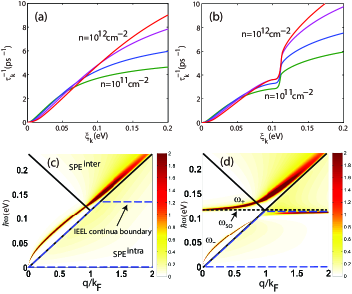
For numerical calculations, the parametersparam corresponding to SiC are used throughout this paper: meV, , , and . Figures 2(a) and (b) show the scattering rates for uncoupled and coupled monolayer graphene as a function of the on-shell energy . As in the case of the 2D electron gas with the parabolic energy dispersion, the scattering rate vanishes at the Fermi energy (i.e., ) and shows the well-known quadratic behavior of near the Fermi energy. Away from the Fermi energy, an upward kink structure appears in the scattering rate for the coupled system, whereas the uncoupled system shows no such structure at any energy. Figures 2(c) and 2(d) show the calculated loss functions –Im of the uncoupled and coupled monolayer graphene for carrier density cm-2 along with the single-particle excitation (SPE) and the injected-electron energy loss (IEEL) continua. The loss function describes electronic energy dissipation and its poles represent the dissipation via plasmon excitations. The intersections of the IEEL continua with the SPE continua indicate the allowed quasiparticle decay via electron-hole pair excitations while the intersections of the IEEL continua with the plasmon lines indicate the allowed quasiparticle decay via the emission of plasmons. Note that the volume of the IEEL continua depends on the energy with which an electron is injected. Hence, an injected electron with a higher energy can have more routes to decay than that injected with a low energy.
For the uncoupled monolayer graphene, the quasiparticle cannot decay via plasmon emission because the plasmon dispersion does not enter the IEEL continua over the whole energy range, as shown in Fig. 2(c). Thus the scattering rate in doped graphene does not show an abrupt increase at any energy.inlife On the other hand, as shown in Fig. 2(d), for the coupled system there are two modes: the phononlike mode and the plasmonlike mode . The plasmonlike mode enters the IEEL continua at a finite critical wave vector .ph_el Thus an additional decay channel via emission is turned on around the SO phonon energy , leading to an upward step in the scattering rate. Note that decay via the emission of the phononlike mode is impossible for monolayer graphene because the mode increases linearly at large with energy slightly higher than that of the uncoupled plasmon mode and thus it does not enter the IEEL continua.
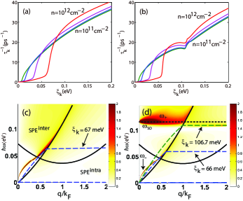
Figure 3 shows the scattering rate and the loss function in uncoupled and coupled bilayer graphene. Unlike the situation with monolayer graphene, the plasmon dispersions for both uncoupled and coupled bilayer graphene enter the IEEL continua. Therefore, even in the uncoupled system the scattering rate exhibits an abrupt increase, which is absent in the uncoupled monolayer system. In addition, while the coupled monolayer graphene system has only a single jump in the scattering rate, the coupled bilayer graphene shows two abrupt jumps. One of them occurs near , for which the emission of the phononlike mode damped in the interband SPE is responsible. The other jump occurs due to the emission of the plasmonlike mode and its threshold energy strongly depends upon the carrier density, hence the emission of the plasmonlike mode is tunable with a carrier density. At higher carrier densities ( the plasmon is strongly coupled to the SO phonon and the threshold energy for the phononlike mode becomes a tunable quantity while the threshold energy for the plasmonlike is fixed around the SO phonon energy .ph_el Note that in bilayer graphene the step of the scattering rate at the phononlike mode shows a weaker density dependence on the carrier density than that in monolayer graphene because of the constant density of states. Also note that our calculation for bilayer graphene is based on the two band model which is valid only at low carrier densities. At high enough carrier densities, the interlayer coupling becomes negligible and the energy band structure of bilayer graphene behaves as a collection of monolayer graphene sheets, thus we expect that the results for bilayer graphene are similar to those of monolayer graphene. At such high densities, the density-dependent jump would disappear and only one single jump around would be found in the scattering rate, as in the monolayer case. We also note that high-energy plasmon modes are known to exist in bilayer graphene.Sensarma2010 ; Gamayun2011 ; Borghi2009 When an electron is injected with sufficiently high energies, a decay through the emission of the high-energy plasmon modes could be possible, leading to additional jumps in the scattering rate. Such jumps are not captured by the two-band effective model and thus beyond the scope of this paper.
III.2 Mean free path
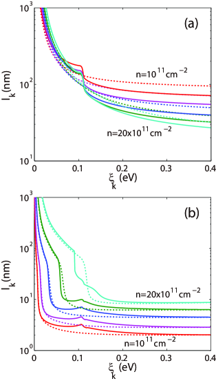
The inelastic mean free paths of the uncoupled and coupled monolayer graphene systems are given in Fig. 4(a). Unlike the uncoupled system, the coupled system shows a sharp decrease in the inelastic mean free path at the SO phonon energy at which the emission of plasmonlike mode is turned on and an electron loses its energy significantly. Thus, by injecting an electron below or above , we can change the mean free path of the system significantly, which can be used for designing a lateral hot electron transistor device in the coupled monolayer graphene system.Palevski1989 ; Sakamoto2000 ; BL Figure 4(b) shows the inelastic mean free path for bilayer graphene systems. The mean free path in bilayer graphene is much shorter than that in monolayer graphene and the step of the mean free path is very small around . Thus the bilayer graphene may not be a good candidate for the application to a lateral hot electron transistor utilizing the electron-phonon interaction. At low energies, however, the inelastic mean free path strongly depends on the carrier density because the threshold energy of the plasmonlike mode is approximately proportional to the Fermi energy. Thus, by changing the carrier density, we can activate or deactivate the decay process via emission of the plasmonlike mode , which is possible even in the uncoupled system without SO phonons. With the help of density tunability through gating, we can achieve a significant change in the mean free path. We find that the mean free path of an electron with an energy eV at the carrier density cm-2 is nm but 1–10 nm at cm-2. This promises a possible use of bilayer graphene as a lateral-hot electron transistor in the absence of electron-SO-phonon coupling.
IV Discussion and Summary
In the previous section we showed the self-energy calculated with dynamical RPA screening. In this section we discuss the effect of dynamical screening of the electron-SO-phonon interaction compared with the results calculated with static screening. We also discuss the effects of finite SO-phonon lifetime and multiple SO-phonon modes of the polar substrate.
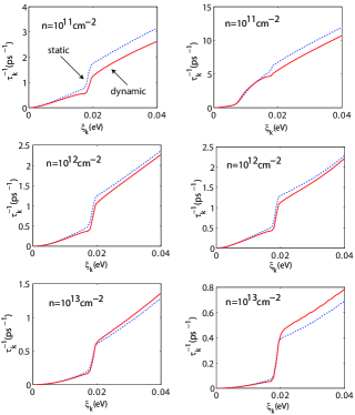
The static screening is equivalent to putting in in Eq. (8), which means that the electrons screen the SO phonons statically, while electron-electron interactions are treated dynamically to take into account the plasmon effects. Figure 5 shows the scattering rates for different carrier densities in monolayer and bilayer graphene with the static or dynamic screening approximations. We find that at low densities the scattering rates with static screening are larger than those with dynamic screening for both monolayer and bilayer graphene, while at high densities the results with dynamic screening are larger than those with static screening. These effects may arise from the attractive nature of the phonon-mediated effective interaction, which originates from the retardation effect coming from the mass difference between ions and electrons. At low densities, the negative contribution to the scattering rate from the attractive effective interaction is significant, and the static screening suppresses the negative contribution more strongly than the dynamic screening, giving a larger scattering rate. As the carrier density increases, the negative contribution to the scattering rate becomes negligible, and the scattering rate with the static screening approximation becomes smaller than that with the dynamic screening, as shown in the bottom panel of 5.
In our calculations, we assume an infinite lifetime for SO phonons because the inclusion of the finite lifetime just suppresses the jumps in the scattering rate without making any qualitative change. Furthermore, the typical decay rates of SO phonons are so small (1 meV) compared to SO phonon energies that the effect of the finite phonon lifetime is quantitatively negligible.
We also assume in our calculations that only one single SO phonon mode is present in substrates. If multiple SO phonon modes exist, as in SiO2, each mode couples to the electron motion independently, giving a jump in the scattering rate near the phonon mode energy. Our results based on one single phonon mode correspond to each of these jumps, and thus extension to multiple phonon modes from our results is trivial.
In conclusion, we theoretically calculated the inelastic scattering rates and the hot-electron inelastic mean free paths for both monolayer and bilayer graphene on a substrate made of polar materials, treating the electron-electron interaction and the electron-SO-phonon interaction on an equal footing. In our theoretical calculation, we include the interaction between electrons, SO phonons, and plasmons within the RPA (for dynamical screening and phonon self-energy correction) and within the leading-order self-energy in the effective total interaction. We find that the strong coupling between the SO phonon and the plasmon leads to an additional decay channel for the quasiparticles through the emission of the coupled mode and gives rise to an abrupt increase in the scattering rate, which is absent in the uncoupled system. In monolayer graphene a single jump in the scattering rate occurs around , arising from the emission of the low energy branch of the coupled modes. By varying the energy of an injected electron, we can change the mean free path significantly. In bilayer graphene the emission of both low and high energy branches of the coupled modes contributes to the scattering rate, and gives rise to two abrupt changes in the scattering rate. In particular, in bilayer graphene, the emission of the plasmonlike mode depends strongly on the carrier density while the threshold energy for the emission of the phononlike mode is weakly dependent on the carrier density and fixed at . Utilizing the density dependence of the plasmonlike mode, we can achieve a significant difference in the mean free path by varying the carrier density. With the help of the abrupt changes in and near , our results for both monolayer and bilayer graphene are applicable to making an electronic device by varying the energy of an injected electron near or tuning the carrier density. It may be possible to fabricate a hot-electron transistor device with a sudden onset of negative differential resistance associated with sharp changes in the inelastic mean free path due to electron-coupled-mode scattering of the injected electrons.
Acknowledgements.
This research was supported by the Basic Science Research Program through the National Research Foundation of Korea (NRF) funded by the Ministry of Science, ICT and Future Planning (Grant No. 2012R1A1A1013963 and Basic Science Research Program 2009-0083540).References
- (1) S. Das Sarma, S. Adam, E. H. Hwang, and E. Rossi, Rev. Mod. Phys. 83, 407 (2011).
- (2) A. H. Castro Neto, F. Guinea, N. M. R. Peres, K. S. Novoselov, and A. K. Geim, Rev. Mod. Phys. 81, 109 (2009).
- (3) Y. Wu, Y. Lin, A. a Bol, K. a Jenkins, F. Xia, D. B. Farmer, Y. Zhu, and P. Avouris, Nature 472, 74 (2011).
- (4) J. H. Chen, C. Jang, S. Xiao, M. Ishigami, and M. S. Fuhrer, Nat. Nanotechnol. 3, 206 (2008).
- (5) V. E. Dorgan,M.-H. Bae, and E. Pop, Appl. Phys. Lett. 97, 082112 (2010).
- (6) Z. Fei, G. Andreev, W. Bao, and L. Zhang, Nano Lett. 11, 4701 (2011).
- (7) J. Robinson et al., Nano Lett. 9, 2873 (2009).
- (8) P. Sutter, Nat.Mater. 8, 171 (2009).
- (9) Y. Liu and R. F. Willis, Phys. Rev. B 81, 081406 (2010).
- (10) R. J. Koch, T. Seyller, and J. A. Schaefer, Phys. Rev. B 82, 201413 (2010).
- (11) C. R. Dean et al., Nat. Nanotechnol. 5, 722 (2010).
- (12) S. Ulstrup, M. Bianchi, R. Hatch, D. Guan, A. Baraldi, D. Alfè, L. Hornekær, and P. Hofmann, Phys. Rev. B 86, 161402 (2012).
- (13) L. Wang, I. Meric, P. Y. Huang, Q. Gao, Y. Gao, H. Tran, T. Taniguchi, K. Watanabe, L. M. Campos, D. a Muller, J. Guo, P. Kim, J. Hone, K. L. Shepard, and C. R. Dean, Science 342, 614 (2013).
- (14) A. Principi, M. Carrega, M. B. Lundeberg, A. Woessner, F. H. L. Koppens, G. Vignale, and M. Polini, Phys. Rev. B 90, 165408 (2014).
- (15) K. Zou, X. Hong, D. Keefer, and J. Zhu, Phys. Rev. Lett 105, 126601 (2010).
- (16) T. Ando, A. B. Fowler, and F. Stern, Rev. Mod. Phys. 54, 437 (1982).
- (17) C.-H. Park, N. Bonini, T. Sohier, G. Samsonidze, B. Kozinsky, M. Calandra, F. Mauri, and N. Marzari, Nano Lett. 14, 1113 (2014).
- (18) T. Sohier, M. Calandra, C.-H. Park, N. Bonini, N. Marzari, and F. Mauri, Phys. Rev. B 90, 125414 (2014).
- (19) E. H. Hwang and S. Das Sarma, Phys. Rev. B 77, 115449 (2008).
- (20) S. H. Zhang, W. Xu, F. M. Peeters, and S. M. Badalyan, Phys. Rev. B 89, 195409 (2014).
- (21) Hongki Min, E. H. Hwang, and S. Das Sarma, Phys. Rev. B 83, 161404(R) (2011).
- (22) Dmitri K. Efetov and Philip Kim, Phys. Rev. Lett. 105, 256805 (2010).
- (23) A. Pachoud, M. Jaiswal, P. K. Ang, K. P. Loh, and B. Özyilmaz, Europhys. Lett. 92, 27001 (2010).
- (24) J. M. Dawlaty, S. Shivaraman, M. Chandrashekhar, F. Rana, and M. G. Spencer, Appl. Phys. Lett. 92, 042116 (2008).
- (25) H. Yan, T. Low, W. Zhu, Y. Wu, M. Freitag, X. Li, F. Guinea, P. Avouris, and F. Xia, Nat. Photonics 7, 394 (2013).
- (26) B. A. Mason and S. Das Sarma, Phys. Rev. B 31, 5223 (1985).
- (27) G.D. Mahan, Many Particle Physics, 3rd ed. (Kluwer/Plenum, New York, 2000).
- (28) W.-K. Tse and S. Das Sarma, Phys. Rev. Lett. 99, 236802 (2007).
- (29) J. P. F. LeBlanc, J. P. Carbotte, and E. J. Nicol, Phys. Rev. B 84, 165448 (2011).
- (30) J. P. Carbotte, J. P. F. LeBlanc, and P. E. C. Ashby, Phys. Rev. B 87, 045405 (2013).
- (31) V. W. Brar, M. S. Jang, M. Sherrott, S. Kim, J. J. Lopez, L. B. Kim, M. Choi, and H. Atwater, Nano Lett. 14, 3876 (2014).
- (32) X. Zhu, W. Wang, W. Yan, M. B. Larsen, P. Bøggild, T. G. Pedersen, S. Xiao, J. Zi, and N. A. Mortensen, Nano Lett. 14, 2907 (2014).
- (33) E. H. Hwang, R. Sensarma, and S. Das Sarma, Phys. Rev. B 82, 195406 (2010).
- (34) M. Jablan, M. Soljačić, and H. Buljan, Phys. Rev. B 83, 161409 (2011).
- (35) Z.-Y. Ong and M. V Fischetti, Phys. Rev. B 86, 165422 (2012).
- (36) E. H. Hwang and S. Das Sarma, Phys. Rev. B 87, 115432 (2013).
- (37) B. Scharf, V. Perebeinos, J. Fabian, and I. Žutić, Phys. Rev. B 88, 125429 (2013).
- (38) S. Fratini and F. Guinea, Phys. Rev. B 77, 195415 (2008).
- (39) J. Schiefele, F. Sols, and F. Guinea, Phys. Rev. B 85, 195420 (2012).
- (40) X. Li, E. A. Barry, J. M. Zavada, M. B. Nardelli, and K. W. Kim, Appl. Phys. Lett. 97, 232105 (2010).
- (41) E. McCann, Phys. Rev. B 74, 161403 (2006).
- (42) E. McCann, D. S. L. Abergel, and V. I. Fal’ko, Solid State Commun. 143, 110 (2007).
- (43) R. Jalabert and S. Das Sarma, Phys. Rev. B 40, 9723 (1989).
- (44) E. H. Hwang and S. Das Sarma, Phys. Rev. B 75, 205418 (2007).
- (45) E. H. Hwang and S. Das Sarma, Phys. Rev. B 52, R8668 (1995).
- (46) E. H. Hwang, B. Y.-K. Hu, and S. Das Sarma, Phys. Rev. B 76, 115434 (2007).
- (47) H. Nienhaus, T. U. Kampen, and W. Mönch, Surf. Sci. 324, L328 (1995).
- (48) R. Sensarma, E. H. Hwang, and S. Das Sarma, Phys. Rev. B 82, 195428 (2010).
- (49) Gamayun, Phys. Rev. B 84, 085112 (2011).
- (50) G. Borghi, M. Polini, R. Asgari, and A. H. MacDonald, Phys. Rev. B 80, 241402 (2009).
- (51) A. Palevski, M. Heiblum, C. P. Umbach, C. M. Knoedler, A. N. Broers, and R. H. Koch, Phys. Rev. Lett 62, 1776 (1989).
- (52) T. Sakamoto, H. Kawaura, T. Baba, and T. Iizuka, Appl. Phys. Lett. 76, 2618 (2000).
- (53) W.-K. Tse, E. H. Hwang, and S. Das Sarma, Appl. Phys. Lett. 93, 023128 (2008).