Dispersion engineered silicon nitride waveguides by geometrical and refractive-index optimization
Abstract
Dispersion engineering in silicon nitride () waveguides is investigated through the optimization of the waveguide transversal dimensions and refractive indices in a multi-cladding arrangement. Ultra-flat dispersion of -84.0 0.5 ps/nm/km between 1700 and 2440 nm and 1.5 3 ps/nm/km between 1670 and 2500 nm is numerically demonstrated. It is shown that typical refractive index fluctuations as well as dimension fluctuations during the fabrication of the waveguides are a limitation for obtaining ultra-flat dispersion profiles. Single- and multi-cladding waveguides are fabricated and their dispersion profiles measured (over nearly 1000 nm) using a low-coherence frequency domain interferometric technique. By appropriate thickness optimization, the zero-dispersion wavelength is tuned over a large spectral range in both single-cladding waveguides and multi-cladding waveguides with small refractive index contrast (3 %). A flat dispersion profile with 3.2 ps/nm/km variation over 500 nm is obtained in a multi-cladding waveguide fabricated with a refractive index contrast of 37 %. Finally, we generate a nearly three-octave supercontinuum in this dispersion flattened multi-cladding waveguide.
pacs:
(230.7380), (260.2030), (130.2790).I Introduction
The development of photonic devices using silicon as the optical medium is paving the way for a monolithically integrated optoelectronic platform in a single chip 1 ; 2 ; 3 . Owing to the large nonlinear refractive index of silicon (500 times larger than silica), a number of functionalities based on nonlinear interactions have been demonstrated in recent years, such as Raman lasers, frequency comb generators, parametric amplifiers, miniature oscilloscopes, wavelength converters, etc 4 ; 5 ; 6 ; 7 ; 8 ; 9 ; 10 ; 11 ; 12 ; 13 ; 14 ; 15 . However, silicon is affected by two-photon absorption (TPA) and free carrier absorption (FCA), two undesirable phenomena that limit the amount of power that can propagate in the silicon waveguide, so that TPA and FCA consequently impair the performance of such a material for nonlinear devices 5 . One way to solve this problem is to employ other materials and/or engineer the chromatic dispersion of the waveguide to substantially reduce the power threshold for nonlinear interactions.
In most nonlinear applications (supercontinuum generation, parametric interactions, etc) the most suitable dispersion is low and anomalous over a broadband spectral range, however other applications like frequency comb generation require moderate anomalous dispersion in order to minimze noise buildup 15 . Furthermore, on chip nonlinear pulse compression can require strong normal dispersion over a broadband spectral range. Indeed, chromatic dispersion can be modified by changing the core transversal dimensions of the waveguide 16 ; 17 . However, this procedure has proven to be insufficient if the aim is to control the dispersion profile in an arbitrary way. It has been proposed 18 that adding a thin extra layer of silicon nitride on top of the silicon core can modify the dispersion of the silicon waveguide. This approach has been explored further by using different refractive index arrangements in a multi-cladding configuration 19 ; 20 ; 21 ; 22 ; 23 ; 24 ; 25 ; 26 ; 27 . The first experimental demonstration of dispersion engineering using more than one cladding layer was recently achieved by adding a 60-nm thick Hafnium dioxide layer on top of a silicon nitride core, the outcome being that the dispersion became more anomalous 28 . Although there have been considerable advancements in the field of silicon photonics over the last years 19 ; 20 ; 21 ; 22 ; 23 ; 24 ; 25 ; 26 ; 27 , a systematic investigation of how to engineer chromatic dispersion is still not very advanced in comparison to, for example, the engineering of the dispersion achieved in photonic crystal fibers 29 ; 30 ; 31 ; 32 . Furthermore, due to the high index contrast, silicon waveguides have a strong dispersion (larger than hundreds of ps/nm/km) so that their engineering is strongly sensitive to refractive index and dimension inaccuracies during the fabrication process. Silicon nitride constitutes a promising alternative material to silicon due to the absence of TPA and FCA at all usable infrared wavelengths 23 ; 33 ; 34 and its compatibility with the cost-effective CMOS technology. Due to the smaller refractive index contrast with silica, appears to be a more appropriate material for dispersion engineering than silicon, since typical fabrication inaccuracies will have lower impact on dispersion, as we demonstrate in the following. The aim of this investigation is producing flat dispersion profiles over broad spectral ranges with arbitrary average dispersion (changing continuously from normal to anomalous dispersion) and with waveguide parameters that are realistic from a fabrication point of view.
II Dispersion engineering approach
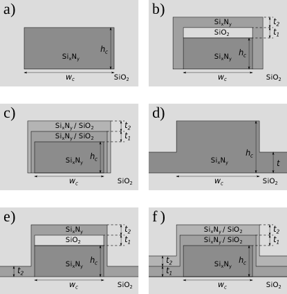
Figure 1 shows the schematics of the cross-section of the waveguides under investigation. There is a substrate layer of silicon (not shown in Fig. 1) with a silica buffer layer of two micron thickness on top of it. These are topped with a silicon nitride core (with width and height ) and a silica upper cladding. Figure 1(a) shows the conventional single-cladding silicon nitride waveguide without any extra cladding layers. In order to engineer the dispersion, part of the upper cladding is modified by including two thin (up to 400 nm) cladding layers, made of silica and/or . The thicknesses of these extra layers are and , and their refractive indices are and . The lateral wall thickness is in all the cases. Two different refractive index arrangements involving the two extra cladding layers are investigated. In the first case, as shown in Fig. 1(b), a high refractive index contrast is considered: for this purpose, the first cladding layer is made of silica and covers only the top of the core, while the second layer is made of . In the second case, as shown in Fig. 1(c), a small refractive index contrast is arranged: the two cladding layers are either or , however there is a refractive index difference of up to 3% between each layer (see Fig. 1c). For these two different refractive index arrangements, four parameters are changed to optimize the dispersion profile: , , , and . Additionally, we analyze whether the inclusion of a rib-like waveguide structure, as schematically shown in Figs. 1(d,e,f), has further effects on the dispersion profile. We finally investigate the effect of the core side-wall angle, which we varied between and .
For the modeling, we employed full vectorial Beam PROP and FemSim packages from commercially available RSoft software. In the first step, we checked the consistency of the calculated dispersion profiles when using both packages, obtaining very good agreement between them 35 . Then, we checked the accuracy of the simulation tool by comparing it with well-known full vectorial analytical solutions of chromatic dispersion in cylindrical optical fibers with a core. Since the numerical accuracy of the algorithm depends on the propagation length and the grid resolution, the simulation was repeated while one of those parameters was increased. Convergence is reached when the effective refractive index stabilizes into a particular value.
The effective refractive index is calculated for the quasi-TE and quasi-TM modes of the designed waveguides. The chromatic dispersion, , is related to the effective refractive index by
| (1) |
where is the wavelength, is the speed of light, and is the effective refractive index. The contribution of material dispersion to the total dispersion is calculated by using the refractive index in equation (1).
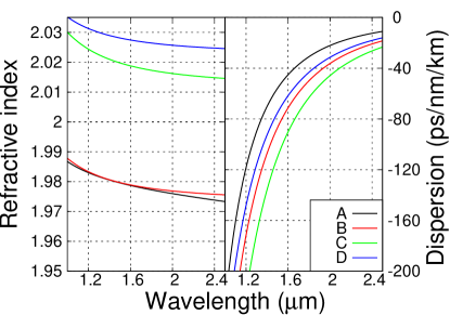
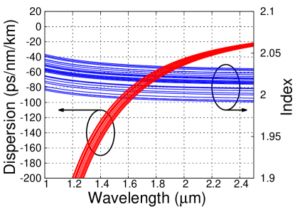
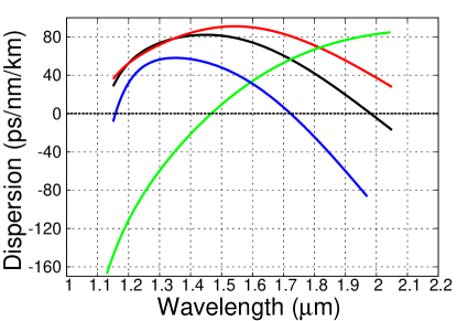
An interesting characteristic of silicon nitride is that its refractive index value can be varied over a fairly large range (1.7 - 2.2) by changing the deposition process. To estimate the impact that refractive index variability has on material dispersion, we compared four different values for the silicon nitride refractive index, as shown in Fig. 2(left). The data depicted with a black line was retrieved from reference 12 and will be called index A, the red line (index B) comes from the Sellmeier equation reported in 36 , the green line (index C) was measured using inline ellipsometry in our fabricated plasma enhanced chemical vapor deposition (PECVD) films, and finally the blue line (index D) comes from 37 . Figure 2(right) shows the calculated material dispersion for the refractive indices A, B, C, and D. At short wavelengths, the material dispersion is strongly dependent on the refractive index characteristics (at 1400 nm, for example, the material dispersion is -75 ps/nm/km for index A and -135 ps/nm/km for index C). This finding indicates that, unlike in the case of silica or silicon, the dispersion can also be engineered by adjusting the deposition process. Due to this variability, the exact refractive index needs to be known in advance with considerable accuracy in order to obtain any specific dispersion profile. In what follows of this paper, unless indicated otherwise, all calculations are performed using the refractive index C and for the fundamental mode. The goal of our calculations is finding the flattest profiles over the largest bandwidth, where the flatness is defined as the smallest variation of the dispersion over a given bandwidth.
III Dispersion engineering in single-clad waveguides by simple geometrical optimization
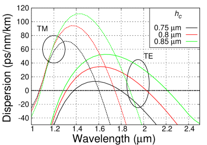
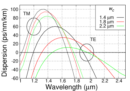
We first review the well known case when no extra cladding layers are added ( for ) and the dispersion is modified solely by changing the width and the height of the core 12 . Since fabricating large values can result in an increase of stress, we only consider the case when is larger than .The chromatic dispersions calculated for a waveguide with width m and heights (black), (red), and m (green) are shown in Fig. 3, while Fig. 4 illustrates the dispersion for a waveguide with height m and widths (black line), (red), and m (green). For comparison purposes, the calculations were done for the quasi-TE (solid lines) and quasi-TM (dotted lines) modes. While the material dispersion is always normal in the near infrared as shown in Fig. 2(right), the strong geometrical dispersion due to the confinement of the light in a waveguide results in a total dispersion that can be anomalous over quite large spectral bandwidths 12 . The dispersion profiles for quasi-TE modes are flatter and tend to shift to longer wavelengths in comparison to the quasi-TM mode profiles. By increasing the core width, the dispersion is vertically down shifted and becomes flatter - an effect that is much stronger for the quasi-TE mode. Furthermore, a small increase of the core height produces a fairly large vertical up-shift of the dispersion profile, while its shape remains unchanged. From the results in Figs. 3 and 4, a basic rule for dispersion engineering can be deduced: a dispersion profile with a given flatness can be vertically shifted by changing .
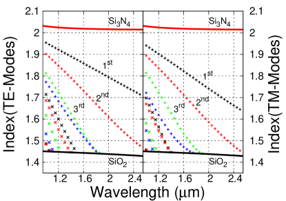
In order to analyze the number of propagating modes supported by the waveguide with and m, the effective refractive indices for the fundamental (1) and high-order modes are calculated for both the quasi-TE (Fig. 5-left) and the quasi-TM (Fig. 5-right) cases. A mode is supported if its effective refractive index value lies between the silicon nitride (red solid line) and silica (black solid line) refractive index values. Note that at 1550 nm, four modes are supported respectively for both the quasi-TE case and the quasi-TM case. The waveguide is single mode at wavelengths beyond m, while at m, up to ten modes can propagate. In what follows of this paper, unless indicated otherwise, the calculations refer to the quasi-TE mode.
IV Dispersion engineering in multi-cladding waveguides with a large () refractive index contrast
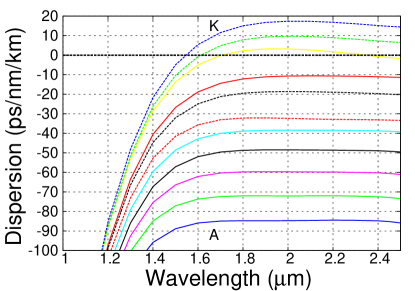
To further engineer the chromatic dispersion, we investigate the arrangement shown in Fig. 1(b), where the cladding layers have a refractive index contrast of : the first cladding is made of silica whereas the second is a silicon nitride layer, while everything is covered by a silica upper cladding. In order to avoid unrealistic dimension values that could produce extremely flat dispersion profiles but could hardly be fabricated, we changed , , and in steps of 10 nm while is changed in steps of 25 nm. As illustrated in Fig. 6, the optimization of the four parameters produces very flat profiles across the 1.65 - 2.5 m spectral region with average dispersion that can be tuned from -85 to +17 ps/nm/km. The third order dispersion is calculated to be = 0.0005 ps/nm2/km at 2 microns for most of the dispersion cases. The dispersion flatness in Fig. 6 is comparable with the flattest dispersion profiles found in photonics crystal fibers 29 ; 30 ; 31 ; 32 .
Table 1 shows the optimized parameters (, , , and ) producing the flattened profiles shown in Fig 6. The one with average dispersion of -85 ps/nm/km is called profile while the one with +17 ps/nm/km is named profile . The remarkable fact from Table 1 is that for a given , a flattened profile can always be engineered by optimizing the , , and values. The optimized values of , , and are ’universally’ valid in the sense that an increase of the value of invariably produces a vertical up-shift of the dispersion, which nonetheless leaves the flatness of the dispersion profile nearly unchanged. Once the optimized , , , and values for flat dispersion are found, a change of is compensated by small changes in the other parameters. By repeating the simulations with other refractive indices, it is found that a vertical up-shift (down-shift) of the profile is always due to an increase (decrease) of . However, as can be expected, the optimal parameters that produce flat dispersion profiles change as the refractive index is changed.
| A | B | C | D | E | F | G | H | I | J | K | |
|---|---|---|---|---|---|---|---|---|---|---|---|
| 1.65 | 1.7 | 1.7 | 1.75 | 1.7 | 1.7 | 1.65 | 1.7 | 1.65 | 1.7 | 1.7 | |
| 0.775 | 0.75 | 0.8 | 0.825 | 0.85 | 0.875 | 0.9 | 0.925 | 0.95 | 0.975 | 1.0 | |
| 0.25 | 0.25 | 0.25 | 0.25 | 0.25 | 0.26 | 0.25 | 0.25 | 0.25 | 0.25 | 0.25 | |
| 0.21 | 0.2 | 0.21 | 0.21 | 0.22 | 0.23 | 0.23 | 0.23 | 0.22 | 0.22 | 0.22 |
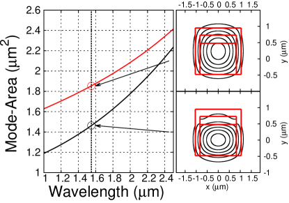
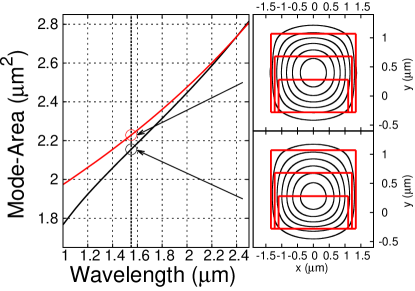
The black line in Figure 7 shows the calculated effective mode-area of a multi-cladding waveguide with identical parameters than the one labelled as C in Fig. 6. For comparison, the red line illustrates the different result obtained when substituting the silica cladding layer by one of silicon nitride. On the right side of Fig. 7, the mode profiles at a wavelength of m are depicted together with the waveguide structure, showing that the field is tightly confined in the core whenever the silica extra cladding layer is included.
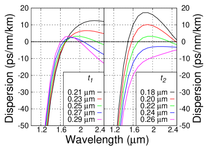
In order to facilitate the design and fabrication of optimized dispersion profiles, it is important to know whether or not it is possible to find simple rules that allow for a predictable modification of the chromatic dispersion. We first checked how dispersion is modified by changing the thickness of the silica cladding layer from to m, as shown in Fig. 8(left). The dispersion profile in green is the same as the one depicted in yellow (profile I) in Fig. 6. As is increased, the dispersion is tilted up for shorter wavelengths, and down for longer wavelengths, while all dispersion profiles intersect at a narrow wavelength region (around m) 20 ; 25 . We numerically verified that this intersection point can be tuned over a broad spectral range by changing , , , or . On the other hand, by increasing the dispersion is vertically down-shifted (the black line corresponds to m, while the magenta one refers to m). Since the down-shift of the profile is less pronounced at longer wavelengths, the dispersion flatness can be controlled via a tuning of 20 ; 25 . Results in Fig. 8 show that a proper adjustement of and produces a flattened dispersion at spectral regions that can be tailored.
V Dispersion engineering in multi-cladding waveguides with small refractive index contrast
The flat dispersion profiles found in the previous section were obtained using silica and silicon nitride as first and second cladding layers, giving a ratio of their refractive indices of . An important question in this context is how this ratio affects the performance of the engineering process 24 . Therefore, a low-contrast () cladding-refractive-index arrangement is investigated: for the first cladding layer while for the second cladding layer , with being the silicon nitride refractive index of the core. The thicknesses and are varied from to m, and the values of and are scanned to retrieve flat dispersion profiles. Fairly flat profiles were found only for a reduced range of parameters. Figure 9 shows in solid lines those dispersion profiles plotted for m and m, while is varied from to m. The dispersion is fairly flat from to m, although not to the same extent as it is in the higher index contrast case and is not over such a broad bandwidth. In order to understand the real impact of this refractive index gradient on dispersion, we perform the calculation for the same values of , , , and while the refractive index contrast is reduced to zero (i.e. like a single-cladding waveguide with larger and ). The simulation results are shown in dotted lines for comparison: the two extra cladding layers with refractive indices that are 1.5 and 3 % lower than the core produce a small vertical down-shift of the dispersion profile with only a negligible change of its shape. By performing simulations where the , , or parameters are changed, it is found that the retrieved dispersion is always a vertically down-shifted version of the case when the refractive index contrast is set to zero: multi-cladding waveguides with small refractive index contrast have equivalent dispersion profiles than single-cladding waveguides. This is explained as due to the small contribution from geometrical dispersion when the index contrast is small.
The effective mode area as a function of wavelength is plotted in Fig. 10, for both cases (with and without refractive index gradient). The field spatial distribution is very similar for both index arrangements, with a noticeable difference in the mode-area only at short wavelengths.
For completeness, other arrangements involving small refractive index contrasts were analyzed. For example, by choosing and or and , no appreciable improvement is obtained in terms of dispersion control if compared with the single-cladding waveguide 38 . The results in this section show that moderate to large refractive index contrasts between the different layers of the waveguide are required in order to enhance the strength of the geometrical dispersion and produce arbitrary dispersion profiles.
VI Chromatic dispersion of a ’rib-like’ waveguide and the effect of the core sidewall angle
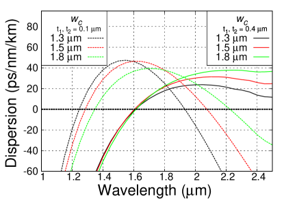
The waveguide geometry can be modified not only by changing and , but also by including a rib-like structure as in Figures 1(d,e,f). The chromatic dispersion is calculated for a waveguide with a rib-like structure like Fig. 1(f) and having m, and m (dotted lines) and m (solid lines). Three cases are considered: , , and m. The profiles in dotted lines show that the inclusion of the rib-like structure makes the dispersion less sensitive to changes of . A comparison of the results in solid lines in Fig. 11 with those in solid lines depicted in Fig. 9 shows that the inclusion of a rib-like structure produces a vertical down-shift of the dispersion as well as a change of its flattness. Therefore, can be used in conjunction with to vertically shift a dispersion profile that has already been engineered. Furthermore, this kind of profile can be used to reduce the impact of dimension fluctuations. On the other hand, we verified that the effect of the lateral wall () is smaller than the effect due to a rib-like structure.
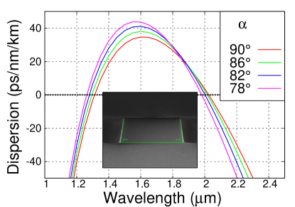
While our numerical analysis considered perfectly rectangular structures, during the fabrication process the resulting waveguides are trapezoidal-like rather than rectangular. As can be seen in the inset of Fig. 12 where the scanning electron microscope (SEM) image of a waveguide is depicted, in our fabricated waveguides the angle is typically rather than . To evaluate the impact of the core side-wall angle, the dispersion is calculated for a single-clad waveguide with m and m. As the angle increases, the dispersion profile is vertically up-shifted and somewhat less flattened. Even though the change is small, it is not negligible and might introduce uncertainty when designing engineered profiles.
VII Impact of variations of the refractive index and geometrical dimensions
VII.1 Fabrication inaccuracies
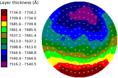
Due to unavoidable uncertainties during the fabrication process of the waveguides, the refractive index and the transversal dimensions might not correspond to what was originally conceived. Consequently, if the fabrication inaccuracies are too large, the designed ultra-flat dispersion profile might not be as flat as initially intended. To assess the impact that refractive index and transversal dimension random fluctuations have on dispersion, several PECVD and films have been grown with a specific thickness and with an uniform refractive index. Both the refractive index and the thickness are measured using in-line ellipsometry at locations evenly scattered over a 200 mm diameter wafer. Figure 13 shows the refractive index for 25 wafer locations as well as their corresponding calculated material dispersions. The refractive index fluctuation (around 2%) will provoke a fluctuation (and therefore an uncertainty) of the dispersion of ps/nm/km at 1550 nm and ps/nm/km at 2500 nm. However, since most of our films exhibited a refractive index fluctuations of 1% over the entire wafer, this fluctuation shall produce a ps/nm/km uncertainty at 1550 nm.
Dimensions inaccuracy during fabrication is another (important) source of dispersion uncertainty. While the targeted thickness of the film was 750 nm, the measured values over the 200 mm wafer scatter from 752 to 776 nm as shown in Fig. 14. However, it is always possible to select a region of the wafer where the thickness corresponds to what was originally intended. Nevertheless, the average offset of 14 nm is an example of a fairly large uncertainty: grown PECVD films with accuracy of 2-3 nm are also very common. These values indicate that the dispersion uncertainty caused by the thickness inaccuracies are of the order of a few ps/nm/km. Note also that the thickness variation over a waveguide scale of a few cm is just nm, therefore no significant dispersion variation might be expected along the length of typical waveguides (a few cm).
VII.2 Chromatic dispersion in multi-cladding waveguides with refractive index fluctuations
Figure 15 illustrates the impact of refractive index fluctuations on the dispersion flatness in a multi-cladding waveguide with refractive index arrangement as in Fig. 1(e). One of the refractive index values from Figure 13 is used for the simulations. The flat dispersion profile (variation of 1.8 ps/nm/km from 1250 to 2500 nm) illustrated by the black line is obtained with m, m, m, and m. Starting from this flat case, we apply an increase of 3% of the refractive index (core and second cladding layer) and a decrease of 3% of the refractive index in the silica cladding layers. The new dispersion profile is depicted with a red line. The flatness is strongly reduced, suggesting that uncontrolled fluctuations of the refractive index during the fabrication of the waveguide might drastically impair the engineering performance. However, by changing the waveguide parameters to m, m, m, and m, it is possible to retrieve again a flat profile as depicted by the green line. Since a 3% refractive index variation is a rather extreme case of fluctuation, it can be concluded that while ultra-flat dispersion profiles (with variations smaller than 1 ps/nm/km) are unlikely to be produced in practice, flat profiles with 5 ps/nm/km variation over hundreds nanometers are realistical to be engineered.
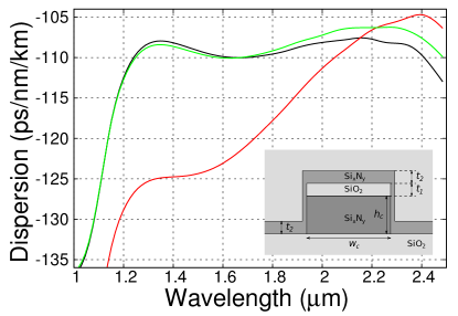
Figure 16 illustrates the impact that a random fluctuation of will have on a flat dispersion profile. The plot in green is the same case than the black plot in Figure 15 and corresponds to m. As is changed, the dispersion profile deviates from the flattest case: a 10 nm deviation of ps/nm/km reduces the bandwidth of flat dispersion from 1000 nm (green) to 800 nm (magenta) or 620 nm (black).
VIII Dispersion measurements of PECVD silicon nitride waveguides
VIII.1 Experimental procedure
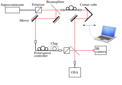
Single- and multi-cladding waveguides having lengths up to 4.85 cm were fabricated using a PECVD process. To tune the chromatic dispersion, different core heights (from to m), core widths (, and m), and thicknesses (from to m, ) were produced. The fabricated waveguides have small or large refractive index contrasts. Using a low-coherence frequency domain interferometric technique 39 , the chromatic dispersion of these waveguides is measured. The experimental arrangement is shown in Fig. 16. The light of a supercontinuum source (SC), spanning from to m, is collimated with an objective, while it is polarized with a broadband polarizer. By rotating the polarizer, we excited either the quasi-TE or the quasi-TM mode of the waveguide. With a beam splitter, the SC light is splitted into the two arms of the interferometer. In one arm (the reference one), a corner cube which is placed on a motorized translation stage allows for the adjustment of the optical path length to obtain the interference pattern. The other arm (the sample arm) contains mirrors to redirect the SC light into an objective that focuses the light in a lensed fibre, finally coupling it into the waveguide under test. An almost identical lensed fibre is placed in the reference arm to compensate for the dispersion of the fibre we use to couple light into the waveguide. In this way, we minimize systematic errors in our measurements by avoiding that the low amount of group delay due to our waveguides is not overwhelmed by the group delay from the lensed fibre. At the waveguide output, an objective is used to collect and collimate the light exiting the chip. A linear polarizer is then used to ensure that only the TE or TM modes are measured. Finally, the light from both arms is combined using a beam splitter, so that the interference signal can be detected using two optical spectrum analyzers (OSAs). The measurement is performed with and without the waveguide in order to substract the group delay due to the unbalanced optical components (fibers, beam splitters, objectives, etc.) in the interferometer. An infrared camera is used to monitor the Gaussian beam profile of the outcoming light. Even though a few modes can propagate in the waveguide, most of the power is coupled into the fundamental mode.
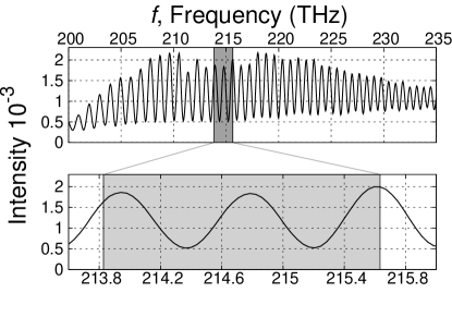
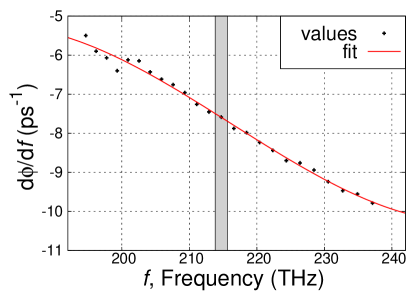
An accurate determination of the dispersion profile requires measuring the interference spectrum over the largest bandwidth possible. Due to the wavelength dependent response of the optical components, we divided the 1000 nm measurement bandwidth in three overlapping spectral sections. Figure 17 shows an example of a typical averaged interference spectrum of one of those three sections. The polarized SC light is aligned with the quasi-TE propagation mode in a single-cladding waveguide (with cm, m and m). The averaging is done using 100 spectra in order to reduce errors from fluctuations of the optical path length in the interferometer. The dependency of the effective refractive index with frequency produces fringes which are not equally spaced. The unequally spaced maxima (or minima) account for a phase difference () as a function of frequency, which is related to the dispersion through . To calculate the dispersion, the spectrum is divided in sub-sections containing a few maxima (three in the case illustrated in Fig. 17), while each subsection is fitted with an appropiate function that allows retrieving values. The black dots in Figure 18 show the retrieved values, while the red curve is the fitting of the data using a third-order polynomial. By taking derivatives of this fitting curve, it is possible to obtain the second- and higher-order dispersion curves for the fabricated waveguides. The Appendix describes in more detail the fitting procedure and the estimated error in the measurement of chromatic dispersion.
VIII.2 Results: single-cladding waveguides and multi-cladding waveguides with small refractive index contrast
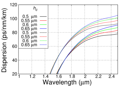
The simulation sections showed that either an increase of or an increase of the and/or in a waveguide with a small refractive index contrast produces a vertical up-shift of the dispersion profile. This up-shift in turn results in a change of the zero dispersion location. Figure 19 shows the measured chromatic dispersion for the quasi-TE mode in waveguides where, through an increase either of the core height or of the cladding layer thickness, the location of the s is progressively shifted. The blue line shows the measured dispersion in a single-cladding waveguide with m and m - there are two s located at 1150 and 1720 nm. The dispersion of a small refractive index contrast waveguide with m, m, and m is plotted with a black line. Because of adding the layers and , the dispersion profile is vertically up-shifted: the is shifted to 1980 nm, while the lies outside of our measurement spectral range but, by extrapolation, is expected to be at 1120 nm. The red line shows the dispersion of a small refractive index contrast waveguide with m, m, and m where the profile is again vertically up-shifted: the is at 2150 nm. Finally, for a waveguide with m, m, and m the profile in green shows that there is only one zero dispersion wavelength ( 1480 nm) at the spectral region of our measurements.
The waveguide parameters for the cases illustrated in black and green lines are identical with the ones in dotted red and solid black lines in the simulation of Figure 11, respectively. The qualitative agreement between both results is excellent: for example, 1480 nm in the green spectrum in Fig. 19 and 1550 nm in the corresponding simulation in Fig. 11 (black solid line). Furthermore, s are located at 1120 and at 1980 nm in the black spectrum in Fig. 19 and at 1280 and at 2060 nm in the corresponding simulation in Fig. 11 (red dashed line). Even though the shape agrees well (but measured profiles are slightly blue-shifted in comparison with simulation), quantitatively, the measured dispersion is higher (80 vs. 45 ps/nm/km) than the simulated one. We believe that this is primarily due to the refractive index uncertainty and also to the uncertainty of the exact waveguide dimensions (estimated to have an error of 5 - 10 nm).
VIII.3 Results: Multi-cladding waveguides with large refractive index contrast
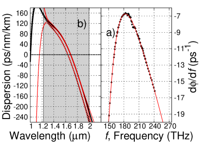
As demonstrated in the simulation sections, a large refractive index contrast is required to have a more arbitrary control of the chromatic dispersion, in particular flat profiles centered at the telecommunication window. Figure 20 shows the measured chromatic dispersion of the quasi-TE mode of multi-cladding waveguides with a refractive index arrangement similar to Fig. 1(e). The inset shows the sketch of the transversal section of the fabricated waveguides. The profile in blue is obtained with waveguide dimensions m, m, nm and nm: Even though the dispersion profile has comparable flatness ( 11 ps/nm/km variation between 1300 and 1800 nm) as in the multi-cladding waveguide with small refractive index contrast, the advantage of having large contrast is that the average dispersion is lower and the mode confinement is tighter. The profile in black ( m, m, nm and nm) has a larger , so that similar flatness to the one in blue is produced while the average dispersion is lower. Finally, a strong increase of and a decrease of ( m, m, nm and nm) results in a much better dispersion optimization - the profile in green is very flat (31 3.2 ps/nm/km) in the region between 1300 and 1800 nm. This flatness is comparable to the ones in state-of-the-art photonic crystal fibers 26 ; 28 .
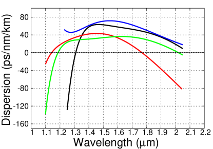
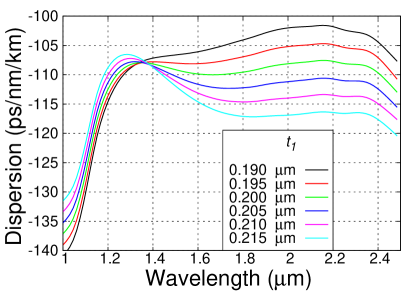
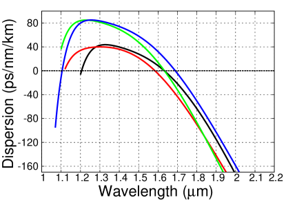
Figure 21 illustrates that even though the dimensions of the fabricated waveguides were chosen to produce flat dispersion profiles for the quasi-TE propagation mode, the multi-cladding arrangement is also advantageous to flatten dispersion for quasi-TM propagation. This is well exemplified with the profile depicted in red which is obtained with the waveguide dimensions m, m, nm and nm and has a dispersion variation of 2 ps/nm/km between 1210 and 1400 nm. The precision of the whole engineering process (fabrication and dispersion characterization) is illustrated by changing by a small amount the waveguide dimensions. The profile in black is obtained with identical dimensions than the one in red except that m: it has similar flatness and shape in comparison with the profile in red, as expected from simulations. Furthermore, from simulations it is expected that a decrease of produces a vertical up-shift of the dispersion profile. In this context, a waveguide having dimensions m, m, nm and nm produces the profile in blue which is vertically up-shifted by 40 ps/nm/km from the previous cases. Finally, the profile in green is with a waveguide with identical dimensions than the one in blue except that m: both profiles have very similar shapes as expected from simulations.
VIII.4 Experimental results: supercontinuum generation in multi-cladding silicon nitride waveguides
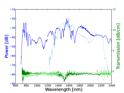
Multi-cladding waveguides with dispersion engineered characteristics should reduce the power threshold for nonlinear interactions. To verify this we propagate a train of 85 fs pulses with a central wavelength at 1560 nm with the aim of generating supercontinuum (SC). Pulses with 90 pJ energy are coupled into the quasi-TE mode of the 1.4 cm long waveguide with a dispersion flattened profile: m, m, nm and nm (its dispersion is depicted with a green line in Figure 20). Two OSAs (one operating from 350 to 1200 nm while the other from 1200 to 2400 nm) are used to acquire the SC spectra. The generated SC is fairly flat and extends nearly over three octaves (from 700 to 2400 nm, limited by the operating bandwidth of the OSA). At 800 nm a strong dispersive wave is generated. This is the broadest SC generated in an integrated waveguide 40 . The dependency of the bandwidth with the dispersion profile is illustrated in the light-blue spectrum which was obtained for the quasi-TM mode of a 1.4 cm long waveguide with m, m, and (its dispersion is depicted in Figure 25) 41 . Due to the much larger and less flat dispersion, the SC spans only between 1250 and 2300 nm. To verify that the different SC bandwidths come from the different dispersion characteristics, the propagation losses are measured by substracting the transmission power in waveguides with different lengths. The losses (peaking at 1520 due to H-N bonds) are similar for both types of multi-cladding waveguides as can be seen in the green line for the waveguide with flat and low dispersion and the light green line for the one with large dispersion.
IX Conclusion
Dispersion engineering by geometrical and refractive index optimization in silicon nitride waveguides was numerically and experimentally investigated. We demonstrated that by incorporating cladding layers with a refractive index ratio of , very flat dispersion profiles can be engineered. For this refractive index ratio, random fluctuations of the waveguide parameters preclude producing ultra-flat dispersion profiles, although profiles with 0.5 ps/nm/km variation are still numerically demonstrated over a 740 nm bandwidth. Single- and multi-cladding waveguides were fabricated and their dispersion profiles measured, showing that flattened profiles are accessible for both quasi-TE and quasi-TM mode propagation. The profiles can be modified with high predictability by changing the core height or the thickness of the cladding layers. A flat dispersion profile with a variation of 3.2 ps/nm/km variation over a 500 nm bandwidth is obtained in a multi-cladding waveguide fabricated with a refractive index contrast of 1.37. The dispersion control characteristics demonstrated here are particularly useful for improving the performance of a number of nonlinear devices and a specific case is analyzed by demonstrating almost three octaves SC generation. This should open new avenues for the advancement of linear and nonlinear functionalities on a chip.
X Acknowledgment
We would like to acknowledge the financial support from the Federal Ministry of Education and Research (BMBF) under grants 03Z2AN11 and 03Z2AN12. Beate Kerpen is gratefully acknowledged for useful comments on the manuscript.
XI Appendix
To determine the chromatic dispersion, we divide the interference pattern in sub-sections containing an appropriate number of maxima (around 2-4) and perform a sinusoidal fit with the following function:
| (2) |
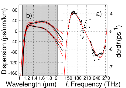
It is assumed that in each sub-section is well represented by , where , is the frequency and is a phase for that subsection. The coefficient is the amplitude of the sinusoidal function, while is an offset to fit the spectrum. The advantage of this fitting function is that it involves the whole interference spectrum, and not only the region where the maxima are located 33 . The black dots in Figures 23(a), 24(a), and 25(a) show examples of retrieved values over a bandwidth of THz. The data is then fitted with a third-order polynomial shown with a red line. By taking the derivative of this polynomial the chromatic dispersion (shown in solid black lines in Figures 23(b), 24(b), and 25(b)) is finally retrieved. The case in Figure 23 corresponds to a waveguide with small refractive-index contrast (as in Fig. 1c) and having m, m. Figure 24 illustrates the very flat dispersion profile case shown in Figure 20 ( m, m, nm, and m). Finally, the Figure 25 shows the profile for the quasi TM mode of a single cladding waveguide with m and m (). Note that in all the cases, the measured shows a dip centered at around 200 THz (1520 nm) which comes from transmission losses due to H-N bonds (see transmission spectrum in Fig. 22). While in the flattened case, changes merely from 4 to 6.5 ps-1 (indicating that the dispersion is low and constant), in the other two cases the change is much bigger (from -6 to -12.5 ps-1 and from from -6.5 to -19.5 ps-1) accounting for a larger chromatic dispersion. Figure 24(a) shows a region between 210 and 220 THz where the measured data cannot be fitted by the third order polynomial - this might be due to the extreme flatness in this waveguide. Furthermore, Figures 23(a), 24(a), and 25(a) indicate that the measurements are expected to be more accurate in determining the zero dispersion wavelength (that occurs when the derivative of is zero) than in determining the maximum of dispersion (that occurs when the second derivative of is zero).
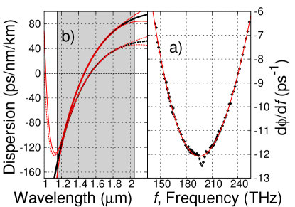
When making the polynomial fitting of , we calculated the curves where there is 95% probability that the measured values will lie within this confidence interval. From these curves, we calculated the red curves in Figures 23(b), 24(b), and 25(b) - the resulting dispersion within the 95% confidence interval is nearly indistinguishable from the original curves (except at the edges) for the large dispersion cases and there is a small difference for the flat and low dispersion case. For comparison purposes, the dotted black lines in Figs. 23(b), 24(b), and 25(b) show the measured dispersion before doing the substraction of the group delay obtained when the waveguide is removed. The difference between solid and dotted lines illustrates the contribution of the group delay from uncompensated optical components in the interferometer, which is important only at long wavelengths.
A comparison of the chromatic dispersion when it was measured over large bandwidths ( nm) and over much shorter ones (e.g. 300 nm) shows that covering both s is the optimal condition for a more accurate dispersion measurement.
References
- (1) G. T. Reed, “Device physics: The optical age of silicon,” Nature, 427, 595-596 (2004).
- (2) B. Jalali, “Teaching silicon new tricks,” Nature Photonics, 1, 193-195 (2007).
- (3) J. Leuthold, C. Koos, and W. Freude, “Nonlinear silicon photonics,” Nature Photonics, 4, 535-544 (2010).
- (4) H. Rong, A. Liu, R. Jones, O. Cohen, D. Hak, R. Nicolaescu, A. Fang, and M. Paniccia, “A continuous-wave Raman silicon laser,” Nature, 433, 725-728 (2005).
- (5) M. A. Foster, A. C. Turner, J. E. Sharping, B. S. Schmidt, M. Lipson, and A. L. Gaeta, “Broad-band optical parametric gain on a silicon photonic chip,” Nature, 441, 960-963 (2006).
- (6) M. R. E. Lamont, B. Luther-Davies, D. Y. Choi, S. Madden, and B. J. Eggleton, “Supercontinuum generation in dispersion engineered highly nonlinear (Gamma = 10 /w/m) As2S3 chalcogenide planar waveguide,” Opt. Express, 16, 14938-14944 (2008).
- (7) J. S. Levy, A. Gondarenko, M. A. Foster, A. C. Turner-Foster, A. L. Gaeta, and M. Lipson, “CMOS-compatible multiple-wavelength oscillator for on-chip optical interconnects,” Nature Photon., 4, 37-40 (2010).
- (8) D. Duchesne, M. Peccianti, M. R. E. Lamont, M. Ferrera, L. Razzari, F. Legare, R. Morandotti, S. Chu, B. E. Little, and D. J. Moss, “Supercontinuum generation in a high index doped silica glass spiral waveguide,” Opt. Express, 18, 923-930 (2010).
- (9) B. Kuyken, S. Clemmen, S. K. Selvaraja, W. Bogaerts, D. Van Thourhout, P. Emplit, S. Massar, G. Roelkens, and R. Baets, “On-chip parametric amplification with 26.5 dB gain at telecommunication wavelengths using cmos compatible hydrogenated amorphous silicon waveguides,” Opt. Lett., 36, 552-554 (2011).
- (10) A. Pasquazi, M. Peccianti, Y. Park, B. E. Little, S. T. Chu, R. Morandotti, J. Azana, and D. J. Moss, “Sub-picosecond phase-sensitive optical pulse characterization on a chip,” Nature Photon., 5, 618-623 (2011).
- (11) F. Ferdous, H. Miao, D. E. Leaird, K. Srinivasan, J. Wang, L. Chen, L. T. Varghese, and A. M. Weiner, “Spectral line-by-line pulse shaping of on-chip microresonator frequency combs,” Nature Photon., 5, 770-776 (2011).
- (12) Y. Okawachi, K. Saha, J. S. Levy, Y. H. Wen, M. Lipson, and A. L. Gaeta, “Octave-spanning frequency comb generation in a silicon nitride chip,” Opt. Lett., 36, 3398-3400 (2011).
- (13) B. Kuyken, X. Liu, G. Roelkens, R. Baets, R. M. Osgood Jr., and W. M. J. Green, “50 dB parametric on-chip gain in silicon photonic wires,” Opt. Lett., 36, 4401-4403 (2011).
- (14) J. S. Levy, M. A. Foster, A. L. Gaeta, and M. Lipson, “Harmonic generation in silicon nitride ring resonators,” Opt. Express, 19, 11415-11421 (2011).
- (15) T. Herr, K. Hartinger, J. Riemensberger, C. Y. Wang, and M.J. Kippenberg, “Universal formation dynamics and noise of kerr-frequency combs in microresonators,” Nature Photon., 6, 480-487 (2012).
- (16) V. R. Almeida, Q. Xu, C. Barrios, and M. Lipson, “Guiding and confining light in void nanostructure,” Opt. Lett., 29, 1209-1211 (2004).
- (17) A. C. Turner, C. Manolatou, B. S. Schmidt, M. Lipson, M. A. Foster, J. E. Sharping, A. L. Gaeta, “Tailored anomalous group-velocity-dispersion in silicon channel waveguides,” Opt. Express, 14, 4357-4362 (2006).
- (18) X. Liu, W. M. Green, I-W. Hsieh, J. I. Dadap, Y. A. Vlasov, and R. M. Osgood Jr, “Conformal dielectric overlayers for engineering dispersion and effective nonlinearity of silicon nanophotonic wires,” Opt. Lett., 33, 2889-2891 (2008).
- (19) E. Dulkeith, F. Xia, L. Schares, W. M. Green, and Y. A. Vlasov, “Group index and group velocity dispersion in silicon on-insulator photonic wires,” Opt. Express, 14, 3853-3863 (2006).
- (20) L. Zhang, Y. Yue, R. G. Beausoleil, and A. E. Willner, “Flattened dispersion in silicon slot waveguides,” Opt. Express, 18, 20529-20534 (2010).
- (21) D. T. H. Tan, K. Ikeda, P. C. Sun, and Y. Fainman, “Group velocity dispersion and self-phase modulation in silicon nitride waveguides,” Appl. Phys. Lett., 96, 061101 (2010).
- (22) S. Mass, J. Caraquitena, J. V. Galan, P. Sanchis, and J. Marti, “Tailoring the dispersion behavior of silicon nanophotonics slot waveguides,” Opt. Express, 18, 20839-20844 (2010).
- (23) L. Zhang, Y. Yan, Y. Yue, Q. Lin, O. Painter, R. G. Beausoleil, and A. E. Willner, “On-chip two-octave supercontinuum generation by enhancing self-steepening of optical pulses,” Opt. Express, 19, 11584-11590 (2011).
- (24) H. Ryu, J. Kim, Y. John, S. Lee, and N. Park, “Effect of index contrasts in the wide spectral-range control of slot waveguide dispersion,” Opt. Express, 20, 13189-13194, (2012).
- (25) M. Zhu, H. Liu, X. Li, N. Huang, Q. Sung, J. Wen, and Z. Wang, “Ultrabroadband flat dispersion tailoring of dual slot silicon waveguide,” Opt. Express, 20, 15899-15907 (2012).
- (26) Y. Yue, L. Zhang, H. Huang, R. G. Beausoleil, and A. E. Willner, “Silicon-on-nitride waveguide with ultralow dispersion over an octave-spanning mid-infrared wavelength range,” IEEE Photonics Journal, 4, 126-132 (2012).
- (27) Y. Yue, L. Zhang, H. Huang, R. G. Beausoleil, and A. E. Willner, “Silicon-on-nitride waveguide with ultralow dispersion over an octave-spanning mid-infrared wavelength range,” IEEE Photonics Journal, 4, 126-132 (2012).
- (28) J. Riemensberger, K. Hartinger, T. Herr, V. Brasch, R. Holzwarth, and T.J. Kippenberg, “Dispersion engineered high-Q silicon nitride ring-resonators via atomic layer deposition,” Opt. Express, 20, 27661-27669 (2012).
- (29) Ferrando, E. Silvestre, and P. Andres, “Designing the properties of dispersion-flattened photonic crystal fibers,” Opt. Express, 9, 687-697 (2001).
- (30) W. H. Reeves, J. C. Knight, P. St. J. Russell, and P. J. Roberts, “Demonstration of ultra-flattened dispersion in photonic crystal fibers,” Opt. Express, 10, 609-613 (2002).
- (31) K. P. Hansen, “Dispersion flattened hybrid-core nonlinear photonic crystal fiber,” Opt. Express, 11, 1503-1509 (2003).
- (32) K. Saitoh, M. Koshiba, T. Hasegawa, and E. Sasaoka, “Chromatic dispersion control in photonic crystal fibers: application to ultra-flattened dispersion,” Opt. Express, 11, 843-852 (2003).
- (33) N. Daldosso, M. Melchiorri, O. Riboli, F. Sbrana, L. Pavesi, G. Pucker, C. Kompocholis, M. Crivellari, P. Bellutti, and A. Lui, “Fabrication and optical characterization of thin two-dimensional si3n4 waveguides,” Mater. Sci. Semicond. Process., 7, 453-458 (2004).
- (34) C. A. Barrios, B. Sanchez, K. B. Gylfason, A. Griol, H. Sohlstrom, M. Holgado, and R. Casquel, “Demonstration of slot-waveguide structures on silicon nitride / silicon oxide platform,” Opt. Express, 15, 6846-6856 (2007).
- (35) F. Fogli, L. Saccomandi, P. Bassi, G. Bellanca, and S. Trillo, “Full vectorial BPM modeling of index-guiding photonic crystal fibers and couplers,“ Opt. Lett., 37, 1685-1687 (2012).
- (36) http://refractiveindex.info/?group=CRYSTALS&material=Si3N4.
- (37) E. D. Palik. Handbook of Optical Constants of Solids. Academic Press, 1985.
- (38) D. Bodenmuller, J.M. Chavez Boggio, H.N.J. Fernando, R. Haynes, and M.M. Roth, “Precise control of the dispersion flatness in silicon nitride waveguides by cladding refractive index engineering,” SPIE Photonics Europe Conference, 2012. SPIE Proceedings vol. 8429, Optical Modelling and Design II, 84290V.
- (39) J.Y. Lee and D.Y. Kim, “Versatile chromatic dispersion measurement of a single mode fiber using spectral white light interferometry,” Opt. Express, 14, 11608-11615 (2006).
- (40) R. Halir, Y. Okawachi, J. S. Levy, M. A. Foster, M. Lipson, and A. L. Gaeta, “Ultrabroadband supercontinuum generation in a CMOS-compatible platform,” Opt. Lett., 37, 1685-1687 (2012).
- (41) J.M. Chavez Boggio, T. Fremberg, D. Bodenmuller, R. Eisermann, L. Zimmermann, D. Gianonne, Y. Hernandez, R. Haynes, and M.M. Roth, “Supercontinuum generation from visible to mid-infrared in a silicon nitride chip” to be submitted to Opt. Exp, 2014.