Reconfigurable photoinduced metamaterials in the microwave regime
Abstract
We investigate optically reconfigurable dielectric metamaterials at gigahertz frequencies. More precisely, we study the microwave response of a subwavelength grating optically imprinted into a semiconductor slab. In the homogenized regime, we analytically evaluate the ordinary and extraordinary component of the effective permittivity tensor by taking into account the photo-carrier dynamics described by the ambipolar diffusion equation. We analyze the impact of semiconductor parameters on the gigahertz metamaterial response which turns out to be highly reconfigurable by varying the photogenerated grating and which can show a marked anisotropic behavior.
I Introduction
Over the past few years the research interest on metamaterial science has shown a sudden increase since metamaterials offer an enormous potential to engineer at will the electromagnetic response. Metamaterials are composite materials built by embedding subwavelength inclusions within a host medium or by depositing them onto a suitable substrate Cai . One of the first metamaterial examples used to mold the light flux to yield a prescribed behavior is Pendry’s lens, a metamaterial device capable of producing sub diffraction-limited images Pendry_1 ; Fang . In order to achieve super-resolution, many authors have suggested structures supporting diffractionless waves such as far-field optical hyperlenses Jacob ; Liu , multilayered metamaterials operating in canalization regime Belov and Kapitza metamaterials Rizza_1 . Metamaterials are characterized by their unusual effective electromagnetic parameters as, for example, very large or very small permittivity or permeability (e.g. epsilon-near-zero or epsilon-infinity media) Elser ; Silveirinha ; Alu_1 ; Jin ; Ciattoni_2 . In addition, chiral Wang and non-reciprocal metamaterials Popa showing strong spatial non-local response have been conceived. On the other hand, exploiting the wide metamaterial flexibility, Pendry et al. proposed transformation optics Pendry_2 as a new scheme to steer light at will. Relevant applications of transformation optics are electromagnetic cloaking and field concentrators Rahma .
Real time tuning of the metamaterial effective electromagnetic response is evidently an important achievement both for conceiving active radiation steering devices and for achieving a dynamical regime where the considered structure can be adapted to a specific task.
Metamaterial tuning methods may be divided into three fundamental classes: (i) circuit tuning methods such as the inclusions of varactor diodes to control the resonant frequency of unit cells, (ii) geometrical tuning methods, which allow to modify the electromagnetic response by changing the geometry (size, orientation, period, etc) of the unit cell, (iii) material tuning methods where a constituent material modifies its electromagnetic response under a suitable external stimulus like light, electric and magnetic field (see Turpin and references therein). Clearly, any tuning technique is suitable for a specific frequency range.
In the Terahertz (THz) frequency region, some researchers are focusing their attention on metamaterial devices containing semiconductor inclusions. Here the device tunability stems from the fact that the semiconductor dielectric response can be adjusted through different mechanisms such as photocarrier injection Padilla_1 ; Shen_1 ; Rizza_2 , application of a bias voltage Chen_1 and thermal excitation Han . This allows to conceive a novel class of photo-generated metamaterials realized without microfabrication processes.
In the case of photocarrier injection, an optical beam with carrier frequency into the absorbtion band generates electron-hole pairs. By spatially modulating the optical beam one can generate a carrier grating able to produce the desired value of permittivity. In Rizza_3 it was shown that a subwavelength photo-generated grating in a GaAs slab can induce a THz metamaterial response ranging from birefringent to hyperbolic to anisotropic negative dielectric. Photo-induced metamaterials have also been used to manipulate the polarization of THz pulses with subcycle switch-on times Kamaraju , while active control of THz optical activity has been achieved by means of chiral photo-induced metamaterials Kanda .
Photo-induced metamaterials are characterized by a pronounced spatial and temporal reconfigurability being obtained without any material structuring (as opposed to the standard metamaterials requiring fabrication).
In this paper we show that the method of Rizza_3 can be extended to the microwave regime where, to the best of our knowledge, photoinduced metamaterials have not yet been studied, although it is worth noting that several authors proposed millimeter-wave manipulation by light control of a semiconductor substrate Lee_1 ; Manasson_1 ; Manasson_2 ; Gallacher . We stress that reconfigurable photo-induced metamaterials in the microwave regime can offer significant potential to achieve novel electromagnetic multifunction applications such as, for example, dynamically photo-excited low reflection metamaterials and shielding panels DePaulis , adaptive perfect lenses lens , active polarizers Kamaraju and actively controllable cloaking devices cloak .
We consider a photo-induced grating, imprinted into a silicon slab by using a spatial light modulator (SLM), whose period is much smaller than the gigahertz (GHz) wavelength. We analytically describe the coupling of optical beam and free carriers and we derive the effective permittivity tensor describing the homogenized metamaterial response. We specifically focus on the impact of semiconductor parameters (diffusion , free carrier life-time , surface recombination velocity ) on the homogenized response. Finally, thanks to the vast tunability offered by the setup, we show that the proposed photoinduced metamaterials can exhibit an extremely anisotropic response.
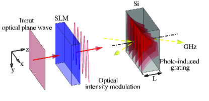
The proposed approach to obtain and test reconfigurable metamaterials consists of a two-stage process: (i) an optical writing phase and (ii) a microwave readout phase. As depicted in Fig. 1, an optical beam is modulated through a SLM and it is launched onto a silicon slab. (i) The optical beam generates free charges and writes a carrier photo-induced grating. (ii) In a second stage, the gigahertz waves reads the imprinted dielectric modulation. By changing the optical illumination, one can reconfigure period and depth of the induced grating to obtain the desired effective microwave response.
The paper is organized as follows. In Sec. II, we describe the spatial dynamics of light and the generated photo-carriers (writing phase). In Sec. III, we discuss the gigahertz response of the photo-induced metamaterials (readout phase). In Sec. IV we consider the impact of the semiconductor parameters on the effective medium response. In Sec. V we compare the predictions of the considered metamaterial description with the results of full-wave simulations. In Sec. VI we draw the conclusions.
II Writing phase
Let us consider a transverse monochromatic optical field (TE) at an angular frequency which, after passing through a spatial light modulator (SLM), impinges on a silicon slab (Si) whose refractive index is , where is the background refractive index, is the absorbtion coefficient, and . In our description of the scattering process of the optical TE wave launched onto the semiconductor, we assume that carrier dynamics do not affect light propagation and the diffraction length is much greater than both the slab thickness and the distance of the spatial light modulator to the vacuum-semiconductor interface.
Under these assumptions, in Appendix A we evaluate the light intensity distribution within the semiconductor slab produced by an arbitrary periodic 1D intensity profile of the impinging optical radiation. The optical beam excites electron-hole pairs and in Appendix B we evaluate the photo-induced carrier density (see Eqs. (18) and (B)) from the ambipolar equation (16) for the intensity profile in the situation where the dependence of both ambipolar diffusion parameter and carrier life-time on carriers densities can be neglected. The appropriate boundary conditions for the ambipolar equation are , where is the surface recombination velocity. Therefore, in our scheme we do not neglect carrier recombination due to impurity centers at the slab surface. As we will show below, such surface effects have a significant impact on the metamaterial effective response.
We focus on the specific and relevant impinging optical illumination
| (1) |
where is the average intensity, and is the modulation period produced by the SLM. The expressions obtained in the Appendices are valid for any slab thickness. However, in the following we will assume that the semiconductor slab thickness is much smaller than the skin depth , i.e. . In this limit we can set equal to 1 the exponential terms in Eq. (15) and, by inserting Eq. (1) in that equation we obtain the following expression for the optical intensity inside the silicon slab
| (2) |
The reflection and transmission coefficients and are complex constants reported in Eqs. (A). In the limit one can further assume that the carrier density profile is uniform along the direction so that the photo-induced grating according to Eq. (18) is
| (3) |
with
| (4) | |||||
| (5) |
The expressions of the effective diffusion lengths and of the constants and are given by Eqs. (20) and (22), respectively, in Appendix B ( is the vacuum impedance, is the reduced Plank’s constant).
III Readout phase
In the readout phase we consider a monochromatic plane wave GHz field (at an angular frequency ) normally impinging onto the silicon slab interface, namely where is a vector lying in the plane and . The GHz dielectric permittivity is described by the Drude model
| (6) |
where is the background dielectric constant, is the electron (hole) density, is the associated effective mass, is the inverse of the relaxation time , is the electric charge unit.
Here we consider the homogenized regime where the period of the photoinduced grating is smaller than the microwave wavelength . In this regime, two GHz plane waves linearly polarized parallel and orthogonal to the axis generally experience different dielectric responses. Through a multiscale technique Felbacq , the effective dielectric permittivity tensor is obtained, where
| (7) |
and is the average of along the -axis. Considering that , ( and are the hole and electron background contributions, respectively) and substituting Eq. (3) into Eq. (6) we obtain
| (8) |
with
| (9) |
Finally, by substituting Eq. (8) into Eq. (7) and performing the spatial averages, we obtain the effective dielectric permittivities components
| (10) |
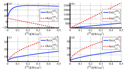
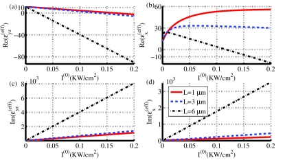
where the sign in the first equation is chosen in such a way that the imaginary part of the effective permittivity is positive as for any passive media. We hereafter set rad/s, rad/s (corresponding to a frequency of GHz and a wavelength m), m, and we consider the following parameters for the silicon slab: , m-1 Vuye , m2/s, m-3, m-3, , ( is the electron mass) Riffe , s, s, .
In Fig. 2 we report the effective parameters characterizing the electromagnetic response as functions of the optical pump intensity with m, m/s, s. More precisely, in Figs. 2(a,b) we plot the effective dielectric permittivities , , and in Figs. 2(c,d) the refractive indices and .
Note that in Fig. 2(a) the real part of the dielectric permittivity reaches its maximum value at kW/cm2 whereas the real part of the dielectric permittivity changes sign at kW/cm2 so that the metamaterial has a hyperbolic response for kW/cm2 .
The marked dependence on the average input intensity of the dielectric permittivity coefficients displayed in Fig. 2 is a very important feature supporting the reconfigurability of the proposed metamaterial setup. In addition, the difference between and significantly increases with , providing the effective medium response a huge uniaxial anisotropy.
IV Dependence of the effective medium response on semiconductor parameters
When , carrier recombination has to compensate photo-generation and the photo-generated carrier density is given by
| (11) |
(see Appendix B) namely is proportional to . Hence, the free carrier life-time becomes a fundamental parameter for achieving an efficient coupling between light and free-carriers.
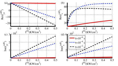
In Fig. 3 we plot the effective dielectric permittivities (with m, m/s) for three different values of that parameter. For s (solid line) the real parts of the effective permittivities are positive in the considered intensity range since the photo-generated carrier modulation is not sufficiently deep to produce metallic regions. For increasing values of the free carrier life-time ( s (dashed line), s (dash-dot line)) the effective medium response anisotropy (with possible hyperbolicity) accordingly grows.
Furthermore the settlement of the free-carrier modulation is affected by the surface recombination velocity and by the semiconductor thickness . The presence of surface impurities reduces the density of the photo-induced carrier and can not be generally neglected.
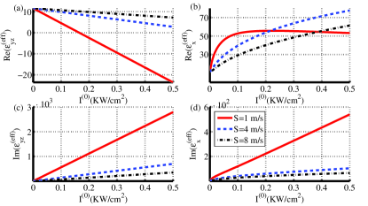
In Fig. 4 we plot the effective dielectric permittivities as functions of the average intensity, for m/s (solid line), m/s (dashed line), m/s (dash-dot line). For low recombination velocities ( m/s), the optical pump illumination produces a deep carrier modulation and the metamaterial anisotropy is accordingly large to the point of showing hyperbolicity (for KW/cm2). On the other hand, for higher recombination velocities ( m/s, m/s), the photo-induced grating is shallow and the real part of the effective permittivity does not change sign in the considered range of illumination intensity ( kW/cm2).
Finally, in Fig. 5 we plot the effective dielectric permittivities as functions of the slab thickness . Such a dependence is specific of the semiconductor based metamaterial we are considering in this paper and it arises from the recombination process occurring at the slab edges. The contribution of the surface recombination is more pronounced the thinner is the semiconductor sample, therefore thinner samples show smaller effective dielectric anisotropy.
V Full-wave simulations
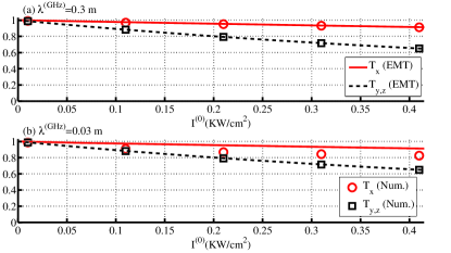
The predictions of the theoretical description illustrated in the previous sections have been checked by evaluating numerically the GHz transmissivity of a semiconductor slab hosting a photo-induced grating. The 2D full-wave simulations have been performed with the comsol RF module com . The integration domain is composed by a semiconductor slab sandwiched by two vacuum layers introduced to provide external excitation and to evaluate the transmissivity.
We have solved Maxwell’s equations for the GHz field (with the Drude dielectric permittivity of Eq. (6)) coupled to the ambipolar diffusion equation (16) with constant and . At the entrance and exit faces (orthogonal to the axis) we used matched boundary conditions on the GHz field to excite a plane wave normally impinging onto the semiconductor slab whereas we imposed the mixed boundary conditions , at the vacuum-semiconductor interfaces. Only one period along the -direction was considered by imposing the continuity conditions at the sides of the unit cell. The numerical simulations have been performed for the parameters used in Fig. 2.
In Fig. 6 we report the slab transmissivities obtained from numerical simulation (circles and squares) for impinging waves linearly polarized along the -axis () and along -axis () and compare them with the transmissivity evaluated using the effective medium theory (solid and dashed lines). In Fig. 6(a) we report such a comparison for the GHz wavelength m and we note that numerical and analytical results are in full agreement. In Fig. 6(b) the same comparison is drawn for m and it reveals slight discrepancies between the two predictions. We explain this discrepancy by observing that, in the first case, the period-wavelength ratio is and the medium dielectric response is fully homogenized whereas, in the second case, so that dielectric homogenization is only partially achieved and contributions due to spatial nonlocality play a role Elser_1 .
VI Conclusions
In conclusions we have theoretically studied the GHz dielectric response of a metamaterial structure suitably photo-induced, and hence highly reconfigurable, by an optical beam within a silicon slab. We have obtained analytical expressions for the components of the effective dielectric tensor in the relevant case of sinusoidal light intensity modulation. We have shown that the GHz effective response has a marked dependence on the optical intensity and it is generally extremely anisotropic. We have also investigated the impact of the semiconductor physical properties (free carrier life-time, surface recombination velocity and slab thickness) on the metamaterial GHz effective response. In view of the high structural reconfigurability of the proposed system and of its extreme metamaterial anisotropy, we believe that our results can be useful to conceive a novel class of active devices to control the GHz field such as polarizers, polarization switchers, filters, lenses and spatial modulators.
Appendix A Optical intensity distribution in the semiconductor slab
As sketched in Fig. 1, we consider an optical plane wave spatially modulated along the -axis by the SLM and normally impinging onto the vacuum-semiconductor interface (at the plane ), namely
| (12) |
We here focus on the situation where the semiconductor slab thickness and the distance between the SLM and the vacuum-semiconductor interface are smaller than the impinging wave diffraction length (where , is the real part of the refractive index and is the scale of the transverse modulation spatially imprinted by the SLM) so that the paraxial approach can be exploited and diffraction can be neglected.
The optical beam inside the semiconductor slab produces an inhomogeneous carrier density distribution (see Appendix B) which in turn affects optical propagation. Under the hypothesis of small refractive index modification, in our approach we neglect such a coupling. The field in the semiconductor slab can be represented as
| (13) |
where and are the slowly varying envelopes of the forward and the backward beams, is the semiconductor refractive index ( is the absorbtion coefficient). Imposing the continuity of electric and magnetic fields at the vacuum-semiconductor interfaces and neglecting diffraction, after some straightforward calculations we analytically obtain the two counterpropagating beams as functions of the incident field and where
| (14) |
so that the optical intensity distribution within the semiconductor slab is
| (15) |
where .
Appendix B Photo-generated carrier density distribution
In the presence of electron-hole generation and recombination processes, the photo-generated carrier density distribution satisfies the -D continuity equation or ambipolar equation solid_book
| (16) |
where is the excess hole density, is the ambipolar diffusion coefficient ( with are the diffusion associated to the electron and hole densities), and are the electron-hole generation and recombination rates, respectively. Note that the rate equation (16) is obtained in the quasi-neutrality condition, namely the excess electrons () and holes () are quasi-equal and the total current density is near zero solid_book . The electron and hole densities are , , respectively where and are the homogeneous background electron and hole densities. The total generation-recombination rate is given by an external contribution due to light absorbtion and a second one accounting for recombination, i.e.
| (17) |
where and is the nonradiative recombination rate coefficient, while the terms containing the coefficients and describe radiative transitions and Auger recombination, respectively Garmire_1 .
We set , assuming that is so small that nonlinear contributions can be neglected, and assuming (i.e. and , ). Under these assumption Eq. (16) becomes a linear equation which, after using Eq. (17) together with the intensity distribution of Eq. (15), can be analytically solved. The periodicity of the optical beam along the -axis allows for a Fourier series expansion of the input intensity distribution where . If we write the carrier distribution as
| (18) |
we get
where the quantities
| (20) |
are effective diffusion lengths. The constant , are fixed by the boundary conditions. By imposing the mixed boundary conditions and at the vacuum-semiconductor interfaces ( is the surface recombination velocity) we obtain
| (21) | |||||
| (22) | |||||
where , , and
| (23) | |||||
| (24) | |||||
| (25) | |||||
References
- (1) W. Cai and V. Shalaev, Optical Metamaterials: Fundamentals and Applications (Springer, Dordrecht, 2010).
- (2) J. B. Pendry, Phys. Rev. Lett. 85, 3966 (2000).
- (3) N. Fang, H. Lee, C. Sun, and X. Zhang, Science 308, 534 (2005).
- (4) Z. Jacob, L.V. Alekseyev, and E. Narimanov, Opt. Expr. 14, 8247 (2006).
- (5) Zhaowei Liu, H. Lee, Y. Xiong, C. Sun and X. Zhang, Science 315 , 1686 (2007).
- (6) P. A. Belov and Y. Hao, Phys. Rev. B 73, 113110 (2006).
- (7) C. Rizza and A. Ciattoni, Phys. Rev. Lett. 110, 143901 (2013).
- (8) J. Elser, R. Wangberg, V.A. Podolskiy, E.E. Narimanov, Appl. Phys. Lett. 89, 261102 (2006).
- (9) M. Silveirinha and N. Engheta, Phys. Rev. Lett. 97, 157403 (2006).
- (10) A. Alu, M. G. Silveirinha, A. Salandrino, and N. Engheta, Phys. Rev. B 75, 155410 (2007).
- (11) Y. Jin and S. He, Opt. Expr. 18, 16587 (2010).
- (12) A. Ciattoni, R. Marinelli, C. Rizza and E. Palange, Appl. Phys. B 110, 23 (2013).
- (13) B. Wang, J. Zhou, T. Koschny, M. Kafesaki and C. M. Soukoulis, J. Opt. A: Pure Appl. Opt. 11, 114003 (2009).
- (14) B. I. Popa and S. A. Cummer, Phys. Rev. B 85, 205101 (2012).
- (15) J. B. Pendry, D. Schurig and D. R. Smith, Science 312, 1780 (2006).
- (16) M. Rahma, D. Schuriga, D. A. Robertsa, S. A. Cummera, D. R. Smitha, J. B. Pendry, Phot. Nano. Fund. Appl. 6, 87 (2008).
- (17) J. P. Turpin, J. A. Bossard, K. L. Morgan, D. H. Werner, and P. L. Werner, International Journal of Antennas and Propagation 2014 429837 (2014).
- (18) W. J. Padilla, A. J. Taylor, C. Highstrete, M. Lee, and R. D. Averitt, Phys. Rev. Lett. 96, 107401 (2006).
- (19) N. Shen, M. Massaouti, M. Gokkavas, J. Manceau, E. Ozbay, M. Kafesaki, T. Koschny, S. Tzortzakis, and C. M. Soukoulis, Phys. Rev. Lett. 106, 037403 (2011).
- (20) C. Rizza, A. Ciattoni, E. Spinozzi, and L. Columbo, Opt. Lett. 37, 3345 (2012).
- (21) H. T. Chen, W. J. Padilla, J. M. O. Zide, A. C. Gossard, A. Taylor, and R. D. Averitt, Nature 444, 597 (2006).
- (22) J. Han and A. Lakhtakia, J. Mod. Opt. 56, 554 (2009).
- (23) C. Rizza, A. Ciattoni, L. Columbo, M. Brambilla and F. Prati, Opt. Lett. 38, 1307 (2013).
- (24) N. Kamaraju, A. Rubano, L. Jian, S. Saha, T. Venkatesan, Jan Nötzold, R. Kramer Campen, M. Wolf and T. Kampfrath, Light: Science & Applications 3, e155 (2014).
- (25) N. Kanda, K. Konishi and M. Kuwata-Gonokami, Opt. Lett. 39, 3274 (2014).
- (26) C. H. Lee and A. P. DeFonzo, IEEE J. Quantum Electron. 16, 277 (1980).
- (27) V. A. Manasson, L. S. Sadovnik, A. Moussessian, and D. B. Rutledge, IEEE Trans. Microw. Theory Tech. 43, 2288, (1995).
- (28) V. A. Manasson, L. S. Sadovnik, V. A. Yepishin, and D. Marker, IEEE Trans. Microw. Theory Tech. 45, 1497, (1997).
- (29) T. F. Gallacher, R. Søndenå, D. A. Robertson and G. M. Smith, IEEE Trans. Microw. Theory Tech. 60, 2301 (2012).
- (30) F. De Paulis, M. H. Nisanci, A. Orlandi, M. Y. Koledintseva, J. L. Drewniak, Electromagnetic Compatibility, IEEE Transactions on, 56, 343 (2014).
- (31) F. Zhang, L. Kang, Q. Zhao, J. Zhou, X. Zhao and D. Lippens, Opt. Express 17, 4360 (2009).
- (32) D. Shin, Y. Urzhumov, Y. Jung, G. Kang, S. Baek, M. Choi, H. Park, K. Kim and D. R. Smith, Nat. Commun. 2, 1213 (2012).
- (33) D. Felbacq, G. Bouchitté, B. Guizal and A. Moreau, J. Nanophotonics 2, 023501 (2008).
- (34) G. Vuye, S. Fisson, V. Nguyen Van, Y. Wang, J. Rivory and F. Abelès, Thin Solid Films 233, 166 (1993).
- (35) D. M. Riffe, J. Opt. Soc. Am. B 19, 1092 (2002).
- (36) COMSOL, www.comsol.com.
- (37) J. Elser, V. A. Podolskiy, I. Salakhutdinov and I. Avrutsky, Appl. Phys. Lett. 90, 191109 (2007).
- (38) G. Grosso and G. Pastori Parravicini, Solid State Physics (Academic Press, San Diego, 2003).
- (39) E. Garmire and A. Kost, Nonlinear Optics in Semiconductors I (Academic Press, 1999).