Compressed optimization of device architectures
Recent advances in nanotechnology have enabled researchers to control individual quantum mechanical objects with unprecedented accuracy, opening the door for both quantumPetta:2005p2180 ; Koppens:2005p717 ; PhysRevLett.108.046808 ; Maune:2012p344 ; Shulman:2012p202 ; Pla:2012p541 ; Kim:2014p70 ; Wu:2014p11938 and extreme-scale conventional computing applicationsFuechsle:2012p242 . As these devices become larger and more complex, the ability to design them such that they can be simply controlled becomes a daunting and computationally infeasible task687879 . Here, motivated by ideas from compressed sensingCandes:2006p1207 ; Donoho:2006p1289 , we introduce a protocol for the Compressed Optimization of Device Architectures (CODA). It leads naturally to a metric for benchmarking device performance and optimizing device designs, and provides a scheme for automating the control of gate operations and reducing their complexity. Because CODA is computationally efficient, it is readily extensible to large systems. We demonstrate the CODA benchmarking and optimization protocols through simulations of up to eight quantum dots in devices that are currently being developed experimentally for quantum computation.
Nanoscale devices are challenging to control in part because their size makes them susceptible to even the smallest material defects. Quantum devices are especially challenging because their energy spectra and tunnel couplings both require fine tuningHanson:2007p1217 . Here we focus on quantum bits (qubits) formed of electron spins in electrostatically-gated quantum dotsLoss:1998p120 and donorsKane:1998p133 . Such devices are extensible to large arrays by leveraging the mature semiconductor processing industry. Working in a variety of systems, researchers have already demonstrated complete control and excellent decoherence properties of devices with up to four quantum dotsPetta:2005p2180 ; Koppens:2005p717 ; PhysRevLett.108.046808 ; Maune:2012p344 ; Shulman:2012p202 ; Medford:2013p654 ; Medford:2013p050501 ; Wu:2014p11938 ; Kim:2014p70 ; Kawakami:2014p666 ; Veldhorst:preprint2013 ; Enge1500214 ; KimNatNano15 ; Kim:2015aa ; PhysRevLett.116.046802 ; 2016arXiv160207833T ; PhysRevLett.116.116801 , as well as impurities coupled to electronic reservoirsPla:2012p541 ; Fuechsle:2012p242 ; Pla:2013p334 ; Muhonen:2014p1402.7140 ; Zwanenburg:2013p961 ; 2015arXiv151201606H ; 0953-8984-27-15-154205 ; Lauchte1500022 .
Processing quantum information in semiconductors requires fine control of the energies and tunnel rates of the individual electrons. Voltages are simultaneously tuned on many electrodes to precisely shape the electrostatic potential landscape within a device. Unfortunately, gate geometries that work well for 1-2 qubits are not necessarily well suited for larger arrays. For example, electrodes designed to control a given dot will also affect its neighbors via capacitive crosstalk. While voltage compensation methods are used to manage crosstalk in smaller devices, hand tuning becomes impractical for larger arrays. Recent methods have been proposed to help automate this process, including optimized randomized benchmarking for immediate tune-up (ORBIT)PhysRevLett.112.240504 , real-time Hamiltonian estimationSchulman:2014unpub , and computer-automated device tuningBaartAPL . While promising, these schemes are either software-based or are only directly applicable to specific device designs. In either case, these schemes are constrained by the capabilities of the quantum device hardware.
In this paper, we aim to make the control problem more tractable through hardware optimization. We show how to modify systematically dot properties, such as occupations, energies, and tunnel rates, while changing as few voltages as possible – a strategy we refer to as control sparsity. The scheme relies on results and methods used for compressed sensingCandes:2006p1207 ; Donoho:2006p1289 in the signal processing literature, in which the decoding of signals can be made much more efficient by exploiting their sparseness. To demonstrate these concepts, we implement the CODA protocol using realistic simulations of several quantum dot devices. We show that CODA yields solutions that are simultaneously sparse and spatially localized near the relevant dot – an extremely desirable property for extensibility. Moreover, formulating control as an optimization problem allows us to directly compare the effectiveness of different device architectures, enabling optimization of the device designs themselves.
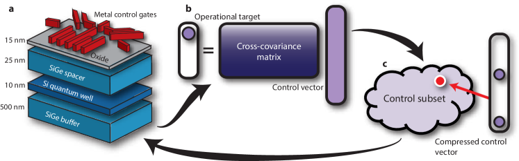
For qubit applications, typical properties we wish to control are the quantum dot occupations and the tunnel rates between the dots, although other properties may also be of interest. Such properties are referred to as operational targets. Generally, an operational target could be composed of several physical attributes; we therefore represent it as a vector in a vector space of outputs . The outputs are determined by the voltages applied to the electrodes and by the device structure. A given set of voltages is referred to as a control setting, represented as a vector in a vector space of controls . A physical system is then representable by a function that maps the controls to the targets: , shown in Fig. 1. Although this mapping is generally nonlinear, for the moment we limit ourselves to a neighborhood in which the mapping is linear, centered around a working point.
In an experiment, it is often the case that one particular operational target needs to be pulsed rapidly, while all the others are held fixed. Since many different can yield a desired , we need both a metric that defines the best and an efficient way to find this control. It is intuitive that solutions are not all equivalently useful: some have extreme voltages that are not experimentally practical, some involve precisely manipulating all the control voltages of the system, while others involve only modest voltages on a few electrodes. The latter scenario describes a desirable property often referred to as “orthogonal” control; i.e., that relatively few electrodes should be involved when trying to change an operational target. Hence, our goal is to identify solutions in which the resulting change in applied voltages is as simple as possible to implement.
This problem is exactly suited to compressed sensing techniques: we are given an underdetermined linear mapping , and we wish to find
| (1) |
where () is the control (target) vector at the working point, () is the control (target) change from the working point, and is the pseudonormDonoho:2006p1289 , which counts the number of non-zero elements in the vector. This type of constrained optimization is known as regularization. Unfortunately, regularization with respect to the pseudonorm is known to be an NP-hard problemNatarajan:1995p227 , so finding a solution is not computationally feasible for large systems. Compressed sensing avoids this difficulty by regularizing the problem using the norm (the sum of the absolute values of the entries of the vector), which is computationally efficient. Regularizing with the norm tends to achieve sparse solutions, while regularizing with the norm (the square root of the sum of the squares of the entries of the vector) does notCandes:2006p1207 ; Donoho:2006p1289 .
Results from compressed sensing show that the control vectors produced by this method are indeed sparseCandes:2006p1207 ; Donoho:2006p1289 ; however, the question of locality has not been addressed. We first give an intuitive argument for why CODA should yield solutions that are local, and then provide a numerical demonstration of the fact. Consider a classical scenario in which the dot couplings are purely capacitive. Since the capacitive coupling between a dot and an electrode decays inversely with separation, electrodes that are far away tend to require large voltage changes to achieve the same response as closer electrodes. Minimizing the norm of the voltage vector suppresses such changes in favor of small voltage changes. In other words, the sparse solutions found by CODA are local.
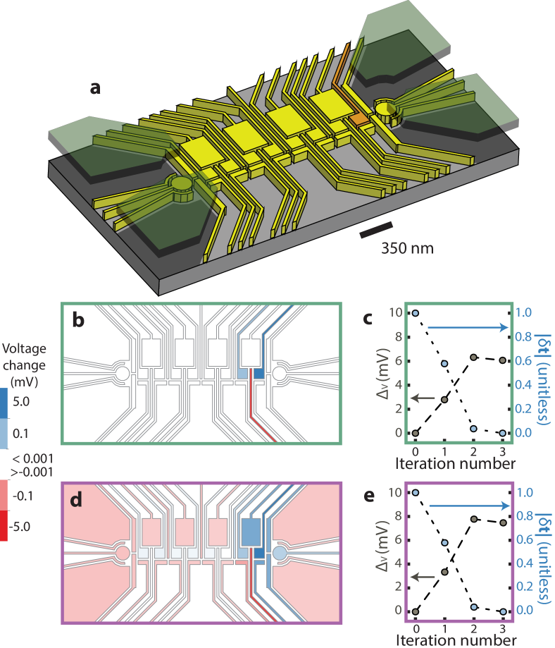
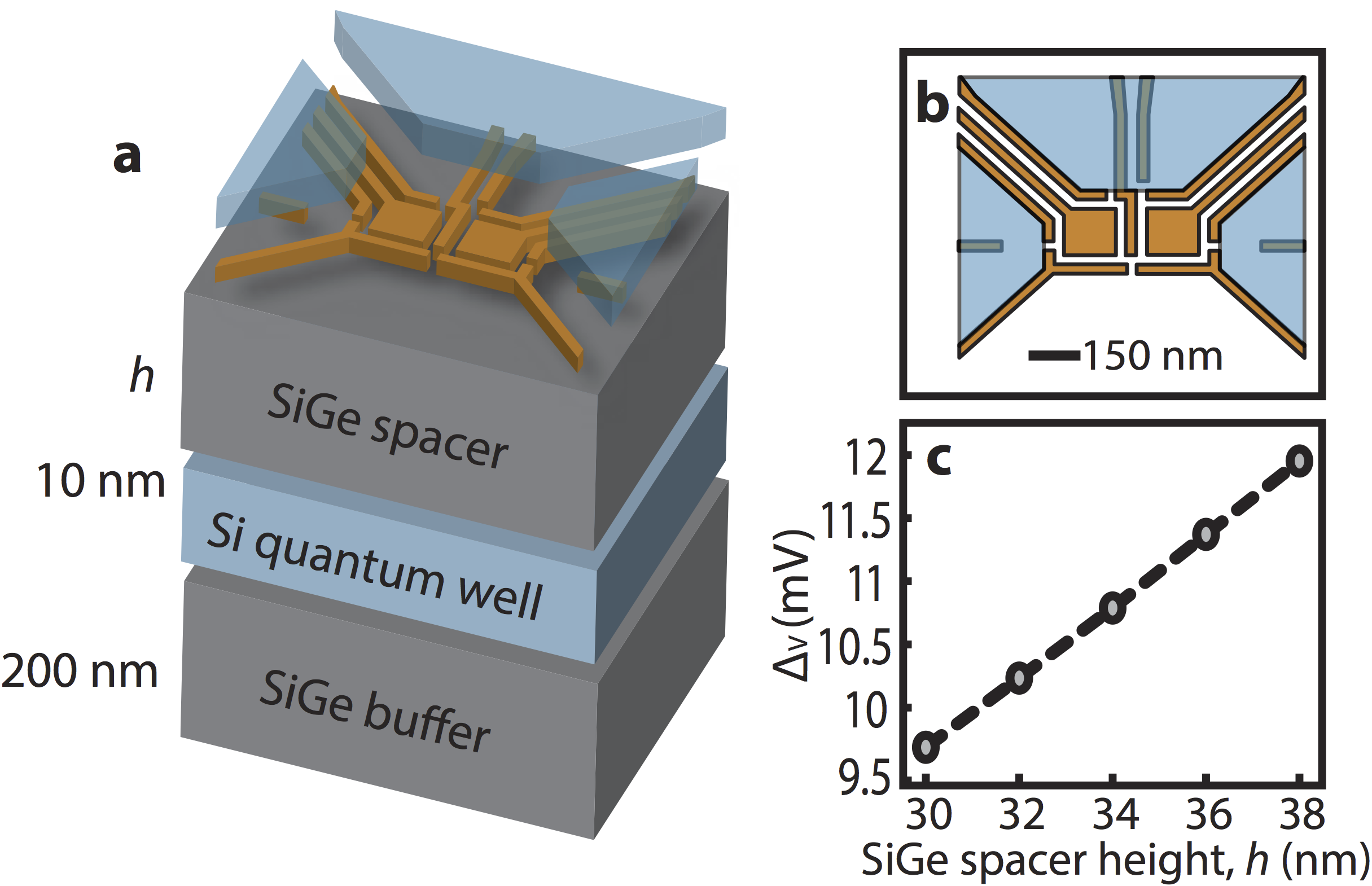
Figure 2 gives a numerical demonstration of the emergence of local solutions when CODA is applied to an accumulation-mode 8-dot device in a Si/SiGe heterostructure with four capacitively coupled double quantum dot qubits. This design represents a natural extension of a recently demonstrated 4-dot device ward:2016 . Figure 2a shows the device design. We model the device using the semiclassical Thomas-Fermi approximationStopa:1996p13767 to compute electron densities and potentials, as described in the Methods. The space of operational targets is defined by the eight dot occupations and the four intra-qubit tunnel rates. Our working point is chosen so there is 1 electron per dot, and energy barriers with maximum heights of 1 meV, corresponding roughly to GHz tunnel rates2015Nanot..26t5703S (see Supplemental Information suppMat for details about the simulation parameters).
We then calculate small changes in the dot occupations and tunnel rates when electrode voltages are varied near the working point, obtaining the cross-covariance matrix that describes the effective linear response of the system. Once the cross-covariance matrix is determined, we may specify a desired output. Here, we focus on the operational target of adding one electron to the right-most quantum dot, while holding all the other tunnel rates and dot occupations constant.
As this is a linear approximation of a non-linear process, a single cycle of the CODA procedure will not necessarily generate voltages which will yield the desired operational target in the device. Regularization therefore requires a closed-loop iteration, as indicated in Fig. 1. To reliably converge, the step size needs to be sufficiently small that the linearized model remains approximately correct. In Fig. 2b, we show the voltage changes needed to achieve convergence of the CODA procedure—in this case, after three iterative steps. Note that although voltages are allowed to vary on all the electrodes, only three voltages are found to vary in the -regularized solution, corresponding to electrodes that are most local to the target of interest. Hence, we confirm that the norm is an effective proxy for local control, and that CODA is a practical tool for tuning a device, because it picks out control solutions that are both sparse and local while achieving a specified operational target. For comparison, we also performed an alternative optimization procedure based on regularization, with results shown in Fig. 2d. Note that although the latter procedure achieves the same target objectives, the solution involves voltage changes on almost all of the electrodes, indicating that this solution is neither local nor sparse.
We now show how CODA can be used to optimize device designs, via the objective comparison of different device designs. We focus on a single double-dot qubit design, shown in Fig. 3a, which can be replicated to form a multi-qubit device. Since CODA automatically localizes the control voltages, using it to design a high-quality unit cell leads naturally to multi-qubit devices that are locally controllable.
We again use the semiclassical Thomas-Fermi approximation Stopa:1996p13767 to model the devices, with working points similar to those used for the 8-dot device. The heterostructure of the simulated devices is shown in Fig. 3a (see Methods for details). To demonstrate how CODA can be used to compare different devices, we consider several devices with the same gate geometry, but with different SiGe spacer heights. In the device with a 30 nm SiGe spacer, we choose an initial working point that corresponds to 1 electron in each quantum dot, and an interdot tunnel barrier of height 1 meV. We next apply the same CODA procedure used in Fig. 2 to add one electron to the right dot, leaving the occupation of the left dot and the tunnel barrier height unchanged. We then increase the spacer height and repeat the procedure. We note here that each new initial working point, corresponding to a new spacer height, was obtained from the previous initial point by allowing CODA to retune the appropriate electrode voltages, yielding a fully automated procedure.
The results of our CODA investigation, shown in Fig. 3, help to compare and contrast the effectiveness of different device designs. Since regularization yields solutions that are local and sparse, we expect that smaller values of will yield devices that are easier to control. In Fig. 3c, we see that reducing the height of the SiGe spacer layer improves the device controllability, as measured by smaller magnitude changes in the control vectors (small ). This is intuitively reasonable because narrow spacers yield strong capacitive couplings between the dots and the top electrodes. In real devices, the advantages of narrow spacers may be offset by the proximity to disorder in the oxide, which is not included in our simulations. However, it is clear that CODA can be an effective tool for assessing designs, and that many types of design questions can be addressed in this way.
In summary, we have introduced a protocol for the Compressed Optimization of Device Architectures, which applies an regularization scheme to a linearized model of device operation. We have demonstrated the effectiveness of this scheme by considering its application to semiconductor nanoelectronic quantum dot systems. As devices continue to grow in complexity, such automated control schemes will be essential for design and operation. Our protocol is computationally efficient to implement, and it provides a systematic approach for achieving local and sparse control. Through realistic semiclassical simulations of double-dot devices, we have illustrated how the CODA scheme can be used for quantitative benchmarking and device development. This method provides a path toward the rational design and operation of extensible quantum nanodevices.
Methods
We perform semi-classical Thomas-Fermi calculationsStopa:1996p13767 using the COMSOL Multiphysics software package to solve a nonlinear Poisson equation in three dimensions. We use zero-field boundary conditions on all sides of the simulated domain, with the exception of the bottom of the SiGe buffer, which is grounded. We assume the following heterostructure profile for all the modeled devices, unless otherwise specified. This profile is consistent with the accumulation-mode devices described in refs. Wu:2014p11938, and Kawakami:2014p666, : 200 nm of Si0.7Ge0.3 (with dielectric constant ), a 10 nm Si quantum well (), 30 nm of Si0.7Ge0.3, 10 nm of Al2O3 (), a 10 nm layer of metallic electrodes, 80 nm of Al2O3, and a second 10 nm layer of metallic electrodes.
The occupations of the dots and the leads are found by integrating the induced 2D charge density over the accumulation regions. The heights of the tunnel barriers are calculated by numerically finding the saddle point over the appropriate potential energy landscape calculated by the self-consistent solver. By changing the voltage on the electrodes, the relevant occupations and tunnel barrier heights can be altered to achieve a desired working point, which in this case consists of one electron per dot and tunnel barrier heights of 1 meV. Small (1 mV) voltage perturbations are then applied to each electrode, and the resulting changes in the operational targets are computed. These data are used to find the mapping in the equation of Eq. 1 (i.e., the cross-covariance matrix).
The and regularized optimization procedures are implemented using the CVXPY computational packageJMLR:v17:15-408 . For additional simulation details, see the Supplemental Information suppMat .
Acknowledgements– The authors thank J. B. Aidun, J. Moussa, N. T. Jacobson, R. P. Muller, and C. Tahan for useful comments and discussions. This work was supported in part by the Laboratory Directed Research and Development program at Sandia National Laboratories and ARO (W911NF-12-1-0607 and W911NF-12-R-0012), NSF (PHY-1104660), ONR (N00014-15-1-0029). Sandia National Laboratories is a multi-program laboratory managed and operated by Sandia Corporation, a wholly owned subsidiary of Lockheed Martin Corporation, for the U.S. Department of Energy’s National Nuclear Security Administration under contract DE-AC04-94AL85000.
Author Contributions– JKG, AF, MF, SNC, RBK, and MAE developed the compressed control scheme. MAE, DRW, and JKG designed the devices. AF and JKG developed and carried out the device simulations. AF, JKG, MF, and SNC wrote the manuscript, with input from all authors.
Competing financial interests– JKG, DRW, MAE, MF, and SNC are co-inventors on a patent application related to some of the nanostructure designs described in this work.
Additional Information– Supplementary information accompanies this paper. Correspondence and requests for materials should be addressed to John King Gamble (jkgambl@sandia.gov).
I Supplemental Information
I.1 CODA procedure
Here, we provide further details about the CODA protocol sketched in Fig. 1 of the main text. Suppose that we have operational targets and controls, and that , so the system is underconstrained. We first identify a working point of experimental interest and assume that perturbations of the device from the working point are small. We then linearize the mapping around ; we express the resulting linear map as a matrix .
In general, we define
| (2) |
where () is the control (target) change from the working point, for is the norm, and is the pseudonormDonoho:2006p1289 , which counts the number of non-zero elements in the vector. Although would be sparse by definition, finding is computationally infeasible for large systems, so we instead find , which tends to be similarly sparse, as shown in the field of compressed sensingCandes:2006p1207 ; Donoho:2006p1289 .
The full protocol for CODA is specified as follows:
-
1.
Identify a working point satisfying . In practice, represents the action of some physical device, and is the computed target vector corresponding to the input control (e.g. voltages).
-
2.
Consider a set of linearly independent, small control variations () about the working point. (We took each to correspond to a small voltage change on a single electrode.) Perform simulations to obtain the resulting data points . Since the control variations were small, by linearity .
-
3.
From the collection of and the associated , construct the linear operator using least squares.
-
4.
For a desired target variation , identify the control variation as defined in Eq. (2). Using a convex program (such as the matrix-free cone solver implemented in the CVXPY packageJMLR:v17:15-408 ), find which has minimal subject to the constraint .
-
5.
Due to the nonlinearity of the system, in general . However, because the linear approximation is valid within a neighborhood around the working point, there must exist a scalar such that . Use a series of simulations to find the maximum value of for which this equation holds, . Define a new control working point , and new desired change in target . Repeat this procedure until convergence is achieved at the final target.
I.2 Simulation details
We perform semi-classical Thomas-Fermi calculationsStopa:1996p13767 using the COMSOL Multiphysics software package to solve a nonlinear Poisson equation in three dimensions. Within the Si quantum well, we define a plane of charge with the charge density given by
| (3) |
where is the charge of an electron, is the transverse effective mass of a conduction electron in silicon, is the strength of the electrostatic potential energy as a function of position, is the Fermi energy (which we take to be at ground), and is the step function. The two prefactors account for the spin and valley degeneracies.
The details of the working point used in the analysis of the 8-dot device are given in the supplemental file 8DotDevice.txt.
In this file, the physical attributes are listed first.
The dot occupations are expressed in electron numbers, and the tunnel barrier heights in eV. Voltages are given for each electrode, with the following labeling convention defined with respect to Fig. 2a of the main text.
Beginning with the upper layer of electrodes, Electrode 1 is in the lower-right corner of the schematic, and the ordering proceeds clockwise.
In the lower layer of gates, Electrode 5 is in the lower-right corner, and the ordering again proceeds clockwise.
Similar details for working points on the devices shown in Fig. 3 are given in the supplemental file VaryingHeight.txt. As before, the dot occupations are given in numbers of electrons and the tunnel barrier heights in eV. Here, the labeling convention for the electrodes begins with the upper layer at the electrode in the upper right corner of the schematic and proceeds clockwise.
On the lower layer of electrodes, the labeling begins at the electrode in the upper-left corner and proceeds clockwise.
Our CODA procedure requires all the components of the control vector to have the same units (and comparable magnitudes for numerical stability). The operational targets considered in our simulations were electron occupations and tunnel barrier heights. To make these quantities comparable for the devices studied here, we multiplied the tunnel barrier height by a factor of 10, to ensure rapid convergence.
References
- (1) Petta, J. R. et al. Coherent manipulation of coupled electron spins in semiconductor quantum dots. Science 309, 2180 (2005).
- (2) Koppens, F. et al. Control and detection of singlet-triplet mixing in a random nuclear field. Science 309, 1346–1350 (2005).
- (3) Prance, J. R. et al. Single-shot measurement of triplet-singlet relaxation in a double quantum dot. Phys. Rev. Lett. 108, 046808 (2012).
- (4) Maune, B. M. et al. Coherent singlet-triplet oscillations in a silicon-based double quantum dot. Nature 481, 344–347 (2012).
- (5) Shulman, M. D. et al. Demonstration of entanglement of electrostatically coupled singlet-triplet qubits. Science 336, 202 (2012).
- (6) Pla, J. J. et al. A single-atom electron spin qubit in silicon. Nature 489, 541–545 (2012).
- (7) Kim, D. et al. Quantum control and process tomography of a semiconductor quantum dot hybrid qubit. Nature 511, 70–74 (2014).
- (8) Wu, X. et al. Two-axis control of a singlet–triplet qubit with an integrated micromagnet. P. N. A. S. 111, 11938–11942 (2014).
- (9) Fuechsle, M. et al. A single-atom transistor. Nature Nano. 7, 242–246 (2012).
- (10) Koza, J. R., Bennett, F. H., Andre, D., Keane, M. A. & Dunlap, F. Automated synthesis of analog electrical circuits by means of genetic programming. IEEE Transactions on Evolutionary Computation 1, 109–128 (1997).
- (11) Candès, E. J., Romberg, J. K. & Tao, T. Stable signal recovery from incomplete and inaccurate measurements. Communications on Pure and Applied Mathematics 59, 1207–1223 (2006).
- (12) Donoho, D. Compressed sensing. IEEE Transactions on Information Theory 52, 1289–1306 (2006).
- (13) Hanson, R., Kouwenhoven, L. P., Petta, J. R., Tarucha, S. & Vandersypen, L. M. K. Spins in few-electron quantum dots. Rev. Mod. Phys. 79, 1217–1265 (2007).
- (14) Loss, D. & DiVincenzo, D. P. Quantum computation with quantum dots. Phys. Rev. A 57, 120–126 (1998).
- (15) Kane, B. E. A silicon-based nuclear spin quantum computer. Nature 393, 133–137 (1998).
- (16) Medford, J. et al. Self-consistent measurement and state tomography of an exchange-only spin qubit. Nature Nano. 8, 654–659 (2013).
- (17) Medford, J. et al. Quantum-dot-based resonant exchange qubit. Phys. Rev. Lett. 111, 050501 (2013).
- (18) Kawakami, E. et al. Electrical control of a long-lived spin qubit in a si/sige quantum dot. Nature Nano. 9, 666–670 (2014).
- (19) Veldhorst, M. et al. An addressable quantum dot qubit with fault-tolerant control fidelity. Nature Nano. 9, 981–985 (2014).
- (20) Eng, K. et al. Isotopically enhanced triple-quantum-dot qubit. Science Advances 1, e1500214 (2015).
- (21) Kim, D. et al. Microwave-driven coherent operation of a semiconductor quantum dot charge qubit. Nature Nano. 10, 243–247 (2015).
- (22) Kim, D. et al. High-fidelity resonant gating of a silicon-based quantum dot hybrid qubit. Npj Quantum Information 1, 15004 (2015).
- (23) Delbecq, M. R. et al. Quantum dephasing in a gated gaas triple quantum dot due to nonergodic noise. Phys. Rev. Lett. 116, 046802 (2016).
- (24) Takeda, K. et al. A fault-tolerant addressable spin qubit in a natural silicon quantum dot (2016). Preprint at http://arxiv.org/abs/1602.07833.
- (25) Martins, F. et al. Noise suppression using symmetric exchange gates in spin qubits. Phys. Rev. Lett. 116, 116801 (2016).
- (26) Pla, J. J. et al. High-fidelity readout and control of a nuclear spin qubit in silicon. Nature 496, 334–338 (2013).
- (27) Muhonen, J. T. et al. Storing quantum information for 30 seconds in a nanoelectronic device. Nature Nano. 9, 986–991 (2014).
- (28) Zwanenburg, F. A. et al. Silicon quantum electronics. Rev. Mod. Phys. 85, 961 (2013).
- (29) Harvey-Collard, P. et al. Nuclear-driven electron spin rotations in a single donor coupled to a silicon quantum dot (2015). Preprint at http://arxiv.org/abs/1512.01606.
- (30) Muhonen, J. T. et al. Quantifying the quantum gate fidelity of single-atom spin qubits in silicon by randomized benchmarking. Journal of Physics: Condensed Matter 27, 154205 (2015).
- (31) Laucht, A. et al. Electrically controlling single-spin qubits in a continuous microwave field. Science Advances 1, e1500022 (2015).
- (32) Kelly, J. et al. Optimal quantum control using randomized benchmarking. Phys. Rev. Lett. 112, 240504 (2014).
- (33) Shulman, M. D. et al. Suppressing qubit dephasing using real-time Hamiltonian estimation. Nat. Commun. 5, 5156 (2014).
- (34) Baart, T. A., Eendebak, P. T., Reichl, C., Wegscheider, W. & Vandersypen, L. M. K. Computer-automated tuning of semiconductor double quantum dots into the single-electron regime. Applied Physics Letters 108, 213104 (2016).
- (35) Natarajan, B. K. Sparse approximate solutions to linear systems. SIAM Journal on Computing 24, 227–234 (1995).
- (36) Frees, A. et al. Supplemental information. Supplemental Information (2016).
- (37) Ward, D. et al. State-conditional coherent charge qubit oscillations in a si/sige quadruple quantum dot. arXiv preprint arXiv:1604.07956 (2016).
- (38) Stopa, M. Quantum dot self-consistent electronic structure and the coulomb blockade. Phys. Rev. B 54, 13767–13783 (1996).
- (39) Shirkhorshidian, A. et al. Transport spectroscopy of low disorder silicon tunnel barriers with and without Sb implants. Nanotechnology 26, 205703 (2015).
- (40) Diamond, S. & Boyd, S. Cvxpy: A python-embedded modeling language for convex optimization. Journal of Machine Learning Research 17, 1–5 (2016).