Cavity QED on a nanofiber using a composite photonic crystal cavity
Abstract
We demonstrate cavity QED conditions in the Purcell regime for single quantum emitters on the surface of an optical nanofiber. The cavity is formed by combining an optical nanofiber and a nanofabricated grating to create a composite photonic crystal cavity. Using this technique, significant enhancement of the spontaneous emission rate into the nanofiber guided modes is observed for single quantum dots. Our results pave the way for enhanced on-fiber light-matter interfaces with clear applications to quantum networks.
Cavity based enhancement of light-matter interactions - referred to as cavity quantum electro-dynamics (QED) - represents a major advance in our ability to control single quantum emitters (QEs) and single photons. One motivation in this field is the possibility of using QEs coupled to cavities as nodes in a quantum network Kimble . Recently, nanophotonic cavity QED devices have attracted great interest PhCReview ; NodaReview , with numerous studies achieving the Purcell regime Purcell of cavity QED for QEs in effective 1D photonic crystal (PhC) cavity structures MangaRao ; LundHansen ; Englund ; Hung ; Thompson .
Among these PhC cavity devices, various types of nanowaveguide cavities have proved to be promising with recent implementations including diamond nanobeams Hausmann , silicon nitride alligator waveguides Goban and PhC nanofiber cavities KaliFIB ; KaliPhC2 . However, for application to quantum networks, in-line (i.e. fiber integrated) light-matter interfaces such as those realized by optical nanofibers are advantageous since automatic coupling to a single mode fiber is achieved Klimov ; LeKienBF ; Chandra ; RauschenbeutelNanoTrap ; KimbleNanoTrap . Although direct fabrication of PhC cavities on nanofibers has seen recent progress KaliPhC2 ; KaliPhC1 ; KaliFIB , designability of the PhC parameters is still limited using this technique.
Here we demonstrate a unique method to achieve cavity QED based enhancement of spontaneous emission (SE) from a single QE on an optical nanofiber. Our method is to create a composite PhC cavity (CPCC) by bringing a nanofiber and a nanofabricated grating with a designed defect into optical contact.
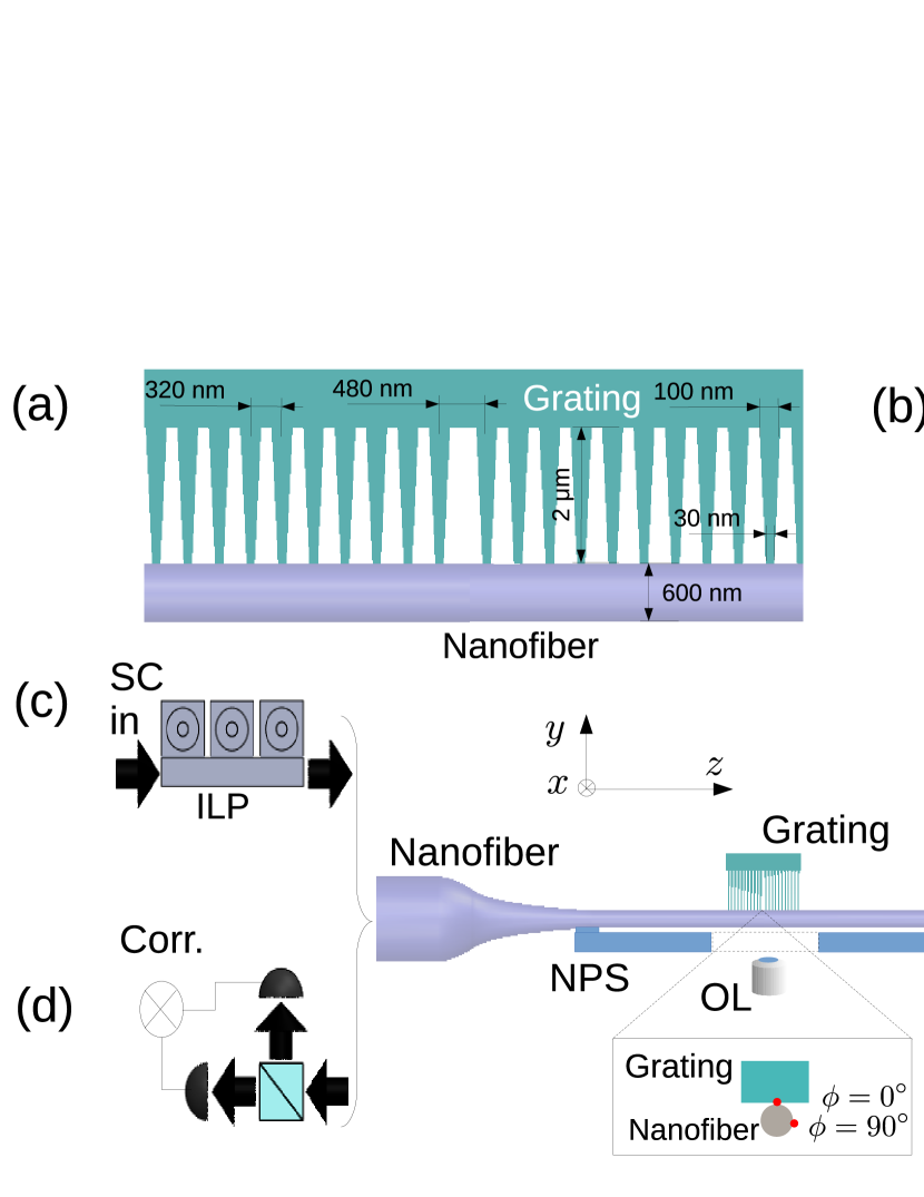
The nanostructured grating as depicted in Fig. 1(a) was designed for an operating wavelength around nm. The grating was fabricated on a silica substrate using electron beam lithography along with chemical etching to create a grating pattern with trapezoidal slats extending m from the substrate. The period of the grating is nm and the slats have a tip width of nm and a base width of nm where and are the grating duty cycles at the tip and base of the slat respectively. In the center of the grating pattern, a defect of width nm was opened between the slats on either side. The number of slats was . The diameter of the nanofiber at the point where the grating was mounted was between 550 nm and 600 nm. Figure 1(b) shows a scanning electron microscope image of the device where the nanofiber can be seen mounted on the grating and crossing the defect region.
Figures 1(c) and 1(d) show the experimental setup for the optical characterization of the CPCC and the measurement of photoluminescence (PL) intensity spectra respectively. In Fig. 1(c), a linearly polarized super-continuum source with an output wavelength range spanning from 700 nm to 1000 nm was introduced to the CPCC via an in-line polarizer. The resulting output spectrum was measured using a Fourier transform spectrum analyser with a resolution of 0.01 nm. We deposited colloidal quantum dots (QDs) with a nominal emission wavelength of 800 nm on the nanofiber by lightly touching the top surface of the nanofiber with a droplet of QD solution ChandraOE . The QDs were thus distributed with an azimuthal position expected to be randomly distributed between and Chandra . The definition of is shown in the inset of Fig. 1(d). The optical loss per deposition was estimated to be 0.6. We estimated the number of QDs by observing the blinking statistics at each deposition. To confirm single QDs, we performed photon correlation measurements using a Hanbury-Brown-Twiss setup as depicted in Fig. 1(d). (Details may be found in Ref. ChandraOE ). The QDs were excited using a 640 nm wavelength laser of power W focused by an objective lens ChandraOE .
Using a nano-positioning stage, we positioned the QD in the center of the excitation spot to better than m by monitoring the QD fluorescence. Through the objective lens, the defect was visible as a line in the center of the grating pattern. We aligned the defect position to within m of the excitation spot center.
To estimate the enhancement of SE, we measured the PL intensity spectrum using an optical multi-channel analyzer (OMA) (Fig. 1(d)). The frequency domain response function of the OMA was measured using a single frequency laser, giving resolutions of nm, nm, and nm, where the superscripts indicate the lines/mm of the OMA gratings. To resolve the polarization dependence of the cavity resonance, we used an OMA resolution of nm. For single QD measurements, we used resolutions of nm and nm to increase the signal-to-noise ratio and to allow accurate determination of the background QD PL intensity. It should be noted that the measured enhancement lineshape is given by , where is the true enhancement spectrum, is the OMA response function and denotes convolution. When , and the height of the measured enhancement peak is reduced by the factor .
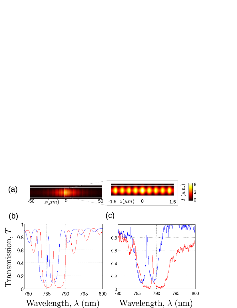
In Fig. 2(a), we show the finite-difference time-domain simulated electric field intensity at the top surface of the nanofiber at a resonance wavelength of nm for the polarized cavity mode (mode). The electric field intensity of the cavity mode reduces exponentially by a factor of over a distance of m from the cavity center. We take the value m as the effective length of the cavity. The inset shows the cavity mode over a region m about the cavity center where the QD is expected to be positioned. It may be seen that the peaks of the cavity mode over this region are approximately of the same intensity with a variation of . This implies that alignment with the exact cavity center is not critical, as any one of the cavity antinodes in this region will lead to approximately the same enhancement of SE.
Due to the asymmetrical index modulation induced by the grating, the degeneracy of the and polarized fundamental modes (- and -modes) of the nanofiber is lifted. Figures 2(b) and 2(c) show simulated and measured cavity transmissions for the and modes (blue and red lines respectively). For the simulations, we set nm. The and mode resonance peaks are separated by 1.3 nm (simulations) and 1.4 nm (experiments). The and mode stop-band minimum transmission values and the mode peak transmission value agree with the simulation values within the experimental error, while the experimental mode transmission is less than the simulation value by . The simulation (measured) and mode quality factors (Q-factors) were () and (). We note that the experimental and simulation results both clearly show that the -mode has a larger Q-factor than the -mode. This is because the -mode experiences more modulation due to the grating leading to larger reflectivity of the Bragg mirrors and thus a higher Q-factor. The experimentally measured and mode resonance peaks have Q-factors about 10 lower than the values predicted by simulations. We also measured the Q-factors for and mode resonance peaks over a range of wavelengths from 780 nm ( nm) to 800 nm ( nm). The Q-factor was found to increase as the wavelength became shorter as we describe later. Additionally, we note that the exact value of for both the and modes is dependent on Mark . By systematically measuring at different , the rate of change was found to be .
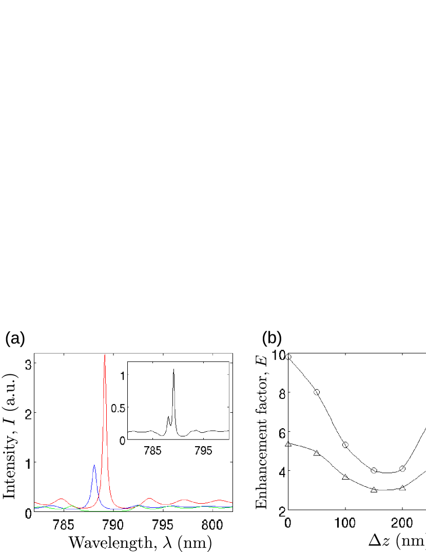
In Fig. 3(a), we show simulated PL intensity spectra through the nanofiber for , , and polarized dipole sources placed at the center of the CPCC for nm. The lack of coupling for the polarized dipole source is caused by the relative phase shift of the component of the cavity mode LeKien . Enhancement factors (EFs) were calculated from the ratio of on- and off-resonance PL intensity spectra. The peak EFs were found to be and for and polarized dipole sources respectively. The mode (mode) enhancement peak has nm ( nm) and the mode (mode) full-width at half-maximum (FWHM) was 0.6 nm (0.4 nm). To simulate the polarization averaged PL intensity spectrum, we averaged the results of Fig. 3(a) (see inset). The average EF was found to be 9.8 at the mode resonance wavelength. The drop in the EF relative to that for a polarized dipole source is due to the increase in the off-resonance background PL intensity due to the contributions of the and polarized dipole sources. By referencing the background PL intensity away from resonance to 0, the ratio of the to mode peak values was calculated to be 3.0.
Figure 3(b) shows simulations of the polarization averaged EF as a function of the displacement from the cavity center for dipole source azimuthal positions with angles of (circles) and (triangles). The solid lines are interpolations to guide the eye. Note that the EF varies from a maximum of 9.8 for at the cavity center to a minimum of 3 for at the first cavity node.
Figure 4(a) shows a typical measured polarization averaged PL intensity spectrum for an OMA resolution of nm and for a number of QDs between 3 and 5 as estimated from blinking statistics ChandraOE . Two enhancement peaks were clearly resolved with nm and nm assigned to the and mode respectively based on independently performed polarization filtered measurements. The mode (mode) FWHM was nm ( nm). Because the spectrum of the QD ( nm FWHM) is broader than the wavelength detection range of the OMA at the nm resolution setting ( nm), the background PL intensity cannot be determined and therefore the EF cannot be calculated. The ratio of the and mode peak values was found to be . The experimentally determined ratio and the enhancement peak wavelength separation show good correspondence with the simulation values. The good agreement between simulations and experimental results suggests that the CPCC functions essentially as designed.
Figure 4(b) shows experimentally measured PL intensity spectra for three different single QDs at different positions on the nanofiber. The off-resonance PL intensity near was normalized to 1. The inset shows a typical anti-bunching signal measured for the deposition where was 795 nm. The normalized intensity correlation function has a zero delay value of indicating a single QD ChandraOE . Sharp enhancement peaks can clearly be seen rising above the broad background PL intensity spectra of the QDs. Although the and mode peaks are not resolved at this OMA resolution ( nm), we assign the peak seen in the PL intensity spectra to the polarized dipole component since the mode peak is larger as seen in Fig. 4(a). The measured EFs were , , and at nm, nm, and nm (black, red and blue curves respectively).
Figure 4(c) summarizes our results regarding the EF for single QDs along with measured Q-factors. The shaded region shows where the EF is expected to lie assuming random placement of the QD in the cavity and randomly distributed between 0∘ and 90∘. The top and bottom black dashed lines, which are estimates of the maximum and minimum simulated EFs respectively (see Fig. 3(c)), are found using a linear fit to simulated EFs at several wavelengths between nm and nm. The simulated EF is seen to increase as becomes shorter. This may be explained by the increase in the Q-factor as shown by the blue triangles in the inset of Fig. 4(c).
The red and green points in Fig. 4(c) show the measured EF as a function of for different single QDs with estimated error bars, for resolutions of nm and nm respectively. Different points at the same wavelength show data taken for separate grating mounting events for the same QD. The variation in the EF may be understood as being due to the variation in the relative position between the QD and the cavity center. We estimate that the positioning accuracy is limited to nm. We note that most of the measured points lie below the shaded region because the resolution limit of the OMA does not allow the true peak amplitude to be measured leading to an underestimate of the EF.
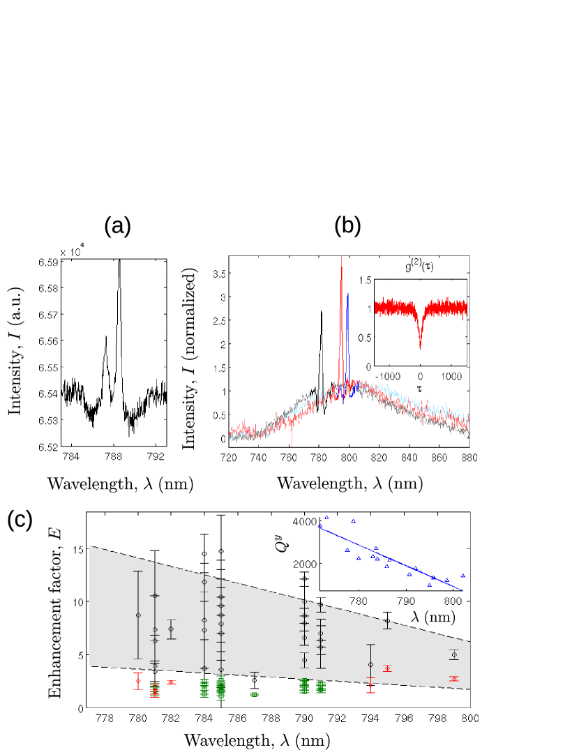
To estimate the true EF, we assumed that , where is the measured FWHM of the mode transmission peak which is non resolution-limited. Using the measured values of , the true EF can be estimated using the formula , where the factors of 1 account for the normalized background at . The black circles in Fig. 4(c) show EFs corrected using the above formula. We note that essentially all the points lie inside the shaded region within the experimental errors.
As seen in Fig. 4(c), we observed EFs which coincided with the maximum value predicted by simulations at values of nm, nm, and nm. This suggests that for these cases, the QD position was close to one of the central cavity antinodes with close to zero. Taking as an example the case where nm, the maximum corrected measured EF was , in good correspondence with the maximum simulation value of .
We note that the EF is given by , where is the decay rate into the guided modes of the CPCC, and is the polarization average of the decay rate into the bare nanofiber guided modes. The factor of arises because all the polarizations contribute to the background PL intensity but only one polarization contributes to the enhancement peak. We can write , where the first bracketed term is the channeling efficiency , the second bracketed term is the Purcell factor , and () is the total (free-space) decay rate of the QE. Note that the EF is not equal to the Purcell factor in general. From the measured EF of as given in the preceeding paragraph, we expect the Purcell factor for a polarized dipole emitter and the channeling efficiency into the nanofiber guided modes to be and respectively at nm from simulations.
On the other hand, in the Purcell regime, is approximately equal to the cooperativity CharmichaelBook . Therefore, we have , where is the QE-cavity coupling, and is the cavity decay rate. It may be shown that for nanofiber cavities, , where is the cavity traversal time LeKien . Using the identity , where is the cavity finesse, the Purcell factor can be expressed as , where . Taking at nm, as calculated by simulations, and as calculated from the experimentally measured mode FWHM, the simulation value for and assuming a nanofiber effective refractive index of , we find , in good agreement with the value of independently calculated in the preceding paragraph.
Note that has a non cavity-dependent component due to the transverse field confinement of the bare nanowaveguide as characterized by , along with a cavity dependent component characterized by . This suggests two routes to achieving better EFs in future CPCC designs: increase the duty cycle or slat number to enhance cavity reflectivity and thus , or reduce the nanofiber diameter thereby increasing . Simulations indicate that using the above strategies, along with a more rectangular slat shape we could achieve a maximum Purcell factor several times larger than the value found in the present study. Such a value would be competitive with PhC cavities in higher refractive index materials Hausmann .
The results presented here demonstrate that it is possible to achieve cavity based enhancement of SE for QEs placed on the surface of a nanofiber. The CPCC method is flexible and can be applied to nanowaveguides other than nanofibers. We anticipate that the composite technique of realizing cavity-enhanced SE on a nanowaveguide as demonstrated here will provide a flexible new tool for future research in PhC cavity enhanced light-matter interactions and may open a new route to the realization of quantum networks.
This work was supported by the Japan Science and Technology Agency (JST) as one of the Strategic Innovation projects.
References
- (1) H. J. Kimble, Nature 453, 1023 (2008).
- (2) J. D. Joannopoulos, P. R. Villeneuve, and S. Fan, Nature 386, 143 (1997).
- (3) S. Noda, M. Fujita, and T. Asano, Nature Photon. 1, 449 (2007).
- (4) E. M. Purcell, Phys. Rev. 69, 681 (1946).
- (5) V.S.C. Manga Rao and S. Hughes, Phys. Rev. B 75, 205437 (2007).
- (6) T. Lund-Hansen, S. Stobbe, B. Julsgaard, H. Thyrrestrup, T. Sünner, M. Kamp, A. Forchel, and P. Lodahl, Phys. Rev. Lett. 101, 113903 (2008).
- (7) D. Englund, B. Shields, K. Rivoire, F. Hatami, J. Vučković, H. Park, and M. D. Lukin, Nano Lett. 10, 3922 (2010).
- (8) C.-L. Hung, S. M. Meenehan, D. E. Chang, O. Painter, and H. J. Kimble, New J. Phys. 15, 083026 (2013).
- (9) J. D. Thompson, T. G. Tiecke, N. P. de Leon, J. Feist, A. V. Akimov, M. Gullans, A. S. Zibrov, V. Vuletic, M. D. Lukin, Science 340, 1202 (2013).
- (10) J. M. Hausmann, B. J. Shields, Q. Quan, Y. Chu, N. P. de Leon, R. Evans, M. J. Burek, A. S. Zibrov, M. Markham, Nano Lett. 13, 5791 (2013).
- (11) A. Goban, C.-L. Hung, S.-P. Yu, J. D. Hood, J. A. Muniz, J. H. Lee, M. J. Martin, A. C. McClung, K. S. Choi, D. E. Chang, O. Painter, H. J. Kimble, Nat. Commun. 5, 4808 (2014).
- (12) K. P. Nayak, Pengfei Zhang, and K. Hakuta , Opt. Lett. 39, 232 (2014).
- (13) K. P. Nayak, F. L. Kien, Y. Kawai, K. Hakuta, K. Nakajima, H. T. Miyazaki, and Y. Sugimoto, Opt. Express 19, 14040 (2011).
- (14) V. V. Klimov and M. Ducloy, Phys. Rev. A 69, 013812 (2004).
- (15) F. L. Kien, S. Dutta Gupta, V. I. Balykin, and K. Hakuta, Phys. Rev. A 72, 032509 (2005).
- (16) R. Yalla, F. L. Kien, M. Morinaga, and K. Hakuta, Phys. Rev. Lett. 109, 063602 (2012).
- (17) E. Vetsch, D. Reitz, G. Sagué, R. Schmidt, S. T. Dawkins, and A. Rauschenbeutel, Phys. Rev. Lett. 104, 203603 (2010).
- (18) A. Goban, K. S. Choi, D. J. Alton, D. Ding, C. Lacroute, M. Pototschnig, T. Thiele, N. P. Stern, and H. J. Kimble, Phys. Rev. Lett. 109, 033603 (2012).
- (19) K. P. Nayak and K. Hakuta, Opt. Express 21, 2480 (2013).
- (20) R. Yalla, K. P. Nayak, and K. Hakuta, Opt. Express 20, 2932 (2012).
- (21) M. Sadgrove, R. Yalla, K. P. Nayak, and K. Hakuta, Opt. Lett. 38, 2542 (2013).
- (22) F. L. Kien and K. Hakuta, Phys. Rev. A 80, 053826 (2009).
- (23) H. J. Charmichael, Statistical methods in quantum optics 2: Nonclassical fields. Springer-Verlag (2008).