Anisotropic Stark effect and electric-field noise suppression for phosphorus donor qubits in silicon
Abstract
We report the use of novel, capacitively terminated coplanar waveguide (CPW) resonators to measure the quadratic Stark shift of phosphorus donor qubits in Si. We confirm that valley repopulation leads to an anisotropic spin-orbit Stark shift depending on electric and magnetic field orientations relative to the Si crystal. By measuring the linear Stark effect, we estimate the effective electric field due to strain in our samples. We show that in the presence of this strain, electric-field sources of decoherence can be non-negligible. Using our measured values for the Stark shift, we predict magnetic fields for which the spin-orbit Stark effect cancels the hyperfine Stark effect, suppressing decoherence from electric-field noise. We discuss the limitations of these noise-suppression points due to random distributions of strain and propose a method for overcoming them.
pacs:
Quantum computing architectures based on donor qubits in siliconKane (1998); Morton et al. (2011); Hill et al. (2005) have generated a great deal of interest due to their long coherence times exceeding seconds in isotopically enriched 28SiTyryshkin et al. (2012); Wolfowicz et al. (2013), scalabilityde Sousa et al. (2004); Hollenberg et al. (2006), and their compatibility with fabrication techniques refined by the Si industry. In many donor-based architectures the mechanism for manipulating individual spins relies on the tuning of a donor in and out of resonance with a global microwave magnetic field. Donor tuning via the Stark shift of Sb donors Bradbury et al. (2006) and As donors Lo et al. (2014) in Si have been studied using electron spin resonance (ESR) techniques Mims (1974); Bradbury et al. (2006). Similarly, strong electroelastic tuning of the hyperfine interaction for P donors in Si has been demonstrated using electrically detected magnetic resonanceDreher et al. (2011).
In the present work, we measure the Stark shift of phosphorus donors in Si using ESR with novel, capacitively terminated, coplanar waveguide (CPW) resonators. These high-sensitivity resonators allow us to measure small spin ensembles subjected to locally homogeneous electric fields. Our measurements resolve a previously predicted anisotropy in the spin-orbit Stark shift due to valley repopulation Rahman et al. (2009); Pica et al. (2014).
It is expected that electric-field noise can contribute substantially to decoherence in the presence of strain. By measuring the linear Stark effect, we estimate the effective electric field due to strain in our devices and the resulting sensitivity of the donors to electric-field noise. From our results we find magnetic fields and crystal orientations where the spin-orbit and hyperfine components of the Stark shift cancel, such that spins are protected from electric-field noise. These “noise-suppression points” are important for near-surface donors and quantum devices incorporating electrostatic gates.
Our experiments were conducted using 1/4-wavelength superconducting CPW resonators operating at 7.1 GHz with Q-factors of 1200. An example is shown in Fig. 1(a). Resonators were patterned from 35 nm thick Nb films deposited on 2 m, P doped, 28Si epilayers (800 ppm 29Si). One end of a resonator is capacitively coupled to a single port transmission line used for exciting the resonator and measuring the spin signal. The other end is capacitively shorted to ground. This capacitive short consists of a 2.9 nF parallel plate capacitor having a plate area of 0.5 mm2. The capacitor is filled with a 17 nm thick atomic layer deposition grown Al2O3 dielectric and satisfies the design rule for a good capacitive short Simons (2001), , where is the resonator frequency, is capacitance, and is the characteristic impedance of the CPW (50 ).
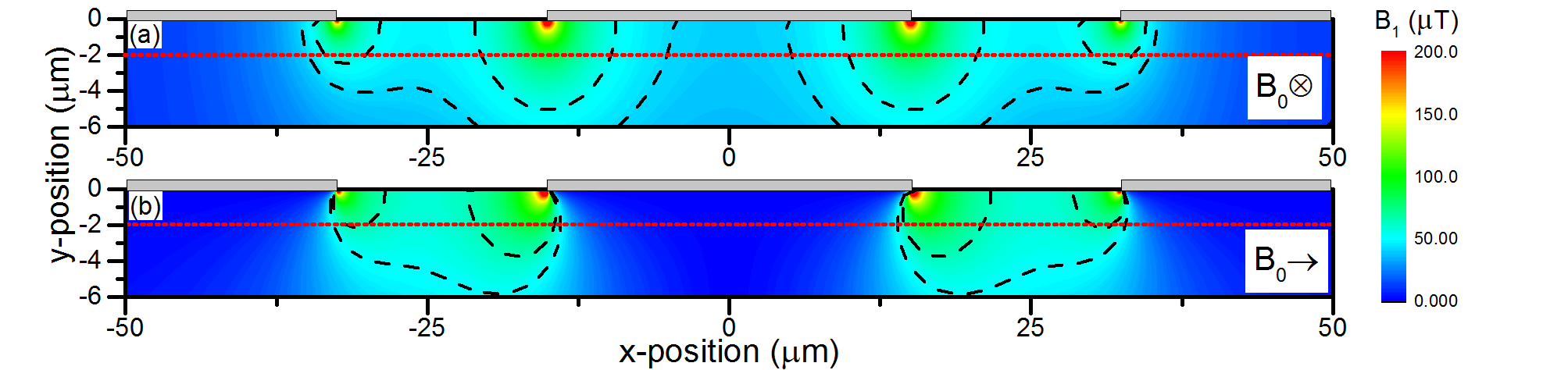
The capacitive short allows the center conductor of the CPW to be biased, providing a direct current (DC) electric field between the center pin and the ground plane of the resonator as shown in Fig. 1(b)-(c). This electric field () is inhomogeneous, except near the plane of the CPW and in the gap between the center pin and the ground plane. To confine spins to these homogeneous regions, we employed a thin, 2 m, phosphorus-doped 28Si epitaxial layer grown on high resistivity p-type Si as our spin ensemble. However, the regions producing the ESR signal vary depending on sample orientation because only the microwave magnetic field () perpendicular to the DC magnetic field () drives spin rotations. The relevant components of are plotted in the supplementary information. We calculated the sub-ensembles of spins contributing to at least half of the signal and they are shaded red in Fig. 1(b)-(c). The weighted electric-field distribution over the subensemble in the case is shown in Fig. 1(d). The standard deviation of the distribution in the x-component magnitude (the dominant component which is directed from the ground plane to the center pin), , is 8% and is approximately the same for .
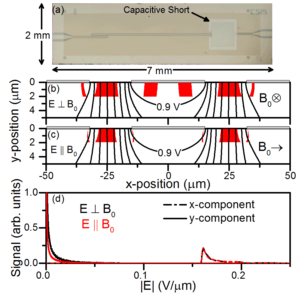
Two sets of resonators were fabricated with center pins oriented parallel to either the 010 or the crystal axes. These orientations place along either the 100 or 110 axes for spins contributing to the ESR signal. The resonators were wire bonded to copper printed circuit boards, connected to a low-noise, cryogenic preamplifier, and placed in a DC magnetic field. With oriented in the plane of the Nb to avoid trapping magnetic flux vortices, devices were cooled to 1.7 K to conduct pulsed ESR experiments.
A pulsed ESR technique sensitive to small resonance shifts Bradbury et al. (2006); Mims (1974) was used to measure the quadratic Stark shift. This technique uses a two-pulse Hahn echo sequence (), with an electric-field pulse applied to the spins during the first dephasing period, . The electric field detunes the spins relative to the driving microwaves such that they accumulate an additional phase, , in the Hahn echo which is measured using a quadrature detector. This experiment utilized bipolar electric-field pulses (pulse sequence IV in Bradbury et al. (2006)) consisting of a positive pulse immediately followed by a negative pulse of the same amplitude and duration. These pulses refocus linear Stark effects (arising from random strain as discussed below) thus allowing the measurement of the quadratic Stark effect. The phase shift is given by
| (1) |
where is the frequency shift of the spins, and are the spin-orbit and hyperfine Stark fitting parameters, respectively, is the electron g-factor, is the Bohr magneton, is the hyperfine coupling constant, is the nuclear spin projection, is the duration of the electric-field pulse, and is the reduced Planck constant Bradbury et al. (2006). A model was developed to simulate the Stark effect in our device including the inhomogeneity in both and . Both fields were computed using a conformal mapping techniqueWen (1969), and each spin’s contribution to the echo was calculated as described in Sigillito et al. (2014). This model also took into account the inhomogeneity present along the length of the CPW. The total echo phase shift of the spin ensemble, , was determined by taking a weighted average of the Stark shift of each spin:
| (2) |
where the sum is taken over all spins, is an amplitude coefficient, is the phase shift of the th spin, is the coupling of the th spin to the resonator, is the microwave magnetic field seen by the th spin, and is the duration of the first microwave pulse in the Hahn echo sequence. In this expression, the term takes into account signal attenuation due to pulse errors arising from inhomogeneity Malissa et al. (2013). We note that the phase shift of a single spin, is not affected by these errors Schweiger and Jeschke (2001).
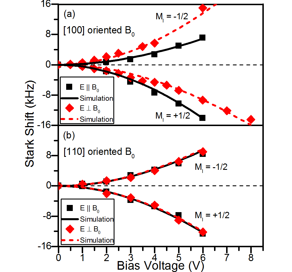
Data for electric fields applied along the 100 and 110 axes with bias voltages up to 8 V are shown in Fig. 2. These data were taken with an electric-field pulse length of and microwave -pulses of . Eq.(2) was fitted to the data and the fitting parameters are given in Table 1. While the hyperfine Stark parameter remains nearly constant, the spin-orbit Stark parameter changes sign and magnitude depending on the electric field orientation relative to and the crystal axis.
| Orientation | Orientation | (/) | (/) | (/) |
|---|---|---|---|---|
| 100 | ||||
| 100 | ||||
| 110 | - | |||
| 110 | - |
Theoretical values are obtained from tight binding calculations reported by Rahman et al. in Rahman et al. (2009).
This anisotropic Stark shift was predicted by Rahman et al. Rahman et al. (2009) and is explained using a valley repopulation model Wilson and Feher (1961). In Si, the g-factor of an electron is related to its effective mass in the direction of . The non-spherical valleys produce a non-uniform effective mass, such that the g-factor of spins in a single valley depends on the angle makes with that valley. In the unperturbed ground state with a symmetric valley combination, the g-factor is equally averaged over all valleys, and no g-factor anisotropy can be resolved. However, when an electric field is oriented along a valley axis (100 for Si), the valley degeneracy is partially lifted, and electrons preferentially fill valleys oriented along the electric field. This changes the effective g-factor and induces an anisotropy in the Stark parameter . The anisotropy is most pronounced when the electric field is oriented along a valley axis. Moreover, application of an electric field in the {111} axes would result in no valley repopulation, since it makes the same angle with all valleys. This orientation is not accessible in our device geometry, but we were able to apply a 110 oriented electric field, and, as expected, the spin-orbit anisotropy became small as shown in Table 1.
It is through the Stark shift that noise can decohere spins and we note the existence of ESR transitions insensitive to this noise. From Eq.(1), we infer that decoherence from noise can differ substantially for the two donor nuclear spin projections, . Moreover, can be tuned such that the first two terms cancel, leading to a transition insensitive to . Due to the dependence of on the orientation of , these noise-suppression points vary with the direction of , and no single can cancel all randomly oriented electric-field noise. For this reason, noise suppression points are most effective in situations where the primary source of noise (and thus the direction of ) is known, such as in gated donor architectures.
In the simplest picture, electric-field noise (which is presumably small) should not contribute to decoherence, since the Stark effect is quadratic. However, this changes dramatically when a large DC electric field (present in gate-addressed architectures) or strain is applied. In this work we consider this field coming from strain Bradbury et al. (2007), inducing a shift in the ESR frequency by modulating the hyperfine interactionDreher et al. (2011) and causing valley repopulationWilson and Feher (1961). The Stark shift in the presence of strain is given as
| (3) |
where is the effective electric field due to strain. When electric-field noise, , is small, the term is negligible whereas the term can be large. Using data in Wilson and Feher (1961), we calculate that a strain of is equivalent to an effective electric field of . We hereafter refer to strain in units of , which corresponds to the strength of .
To investigate strain we use unipolar (positive bias) pulses, instead of the bipolar pulses used to gather the data for Fig. 2. Bipolar pulses cancel the linear term of Eq.(3) whereas unipolar pulses lead to a broadening of the ESR line and loss of signal when internal strains are inhomogeneous across the spin ensemble. Despite this broadening, data were taken using unipolar pulses with amplitudes of up to (supplemental material). These data indicate that strain is approximately in our wafers, and the signal loss indicates that the strain is primarily random. We compare this to a similar sample (10 m P doped epitaxial layer of 28Si) reported Tyryshkin et al. (2006) with an electron nuclear double resonance (ENDOR) linewidth of 100 kHz. Assuming that broadening of the ENDOR line is due primarily to strain, this linewidth corresponds to an distribution spanning , comparable to our results. For these strains, the spins’ sensitivity to electric-field noise, , can be large. The limited coherence time () is inversely proportional to de Sousa (2009) so electric-field sources of decoherence can be substantial. While the contribution to the coherence time will vary from system to system, we calculate (using de Sousa (2009)) that for of noise on our CPW center pin, would be limited to in the devices used in these experiments Devices with gates more strongly coupled to the donors would have their affected more severely.
Internal strains can also lead to errors in measuring , even when using bipolar pulses. This is because depends on the direction of the total electric field which includes . Since is random, there is uncertainty in the actual direction of the total electric field relative to . Care was taken to minimize strain when mounting the devices, but not all strain can be avoided and in our devices we found that was larger than the applied electric fields. The errors arising from strain should become small as becomes large, so data taken at higher bias voltages were weighted more heavily when fitting the model. For our samples we estimate that the magnitude of can be underestimated by up to a factor of 2.5 for the 100 data.
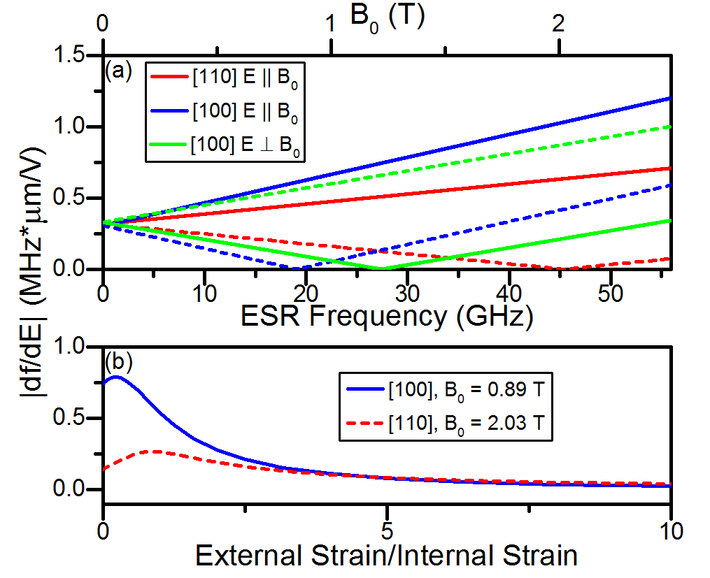
Taking into account strain, we quantitatively compute the sensitivity of spins to electric-field noise (). For the simple case, where the strain is uniform and oriented in the same direction as the , we plot in Fig. 3(a) (assuming is ). noise suppression points appear as minima in . This case applies to bulk 28Si crystals where the strain distribution can be small () and single-donor systems.
We recognize that in devices containing ensembles of spins, randomly oriented strain leads to a distribution in over the ensemble, washing out noise suppression effects. Assuming random strain of order , comparable to the strain in our samples, should on average decrease by a factor of 5 for one hyperfine line compared to the other. This corresponds to an increase in by a factor of 25 (because de Sousa (2009)) as shown in the supplemental information. This implies that, even with the simple approach of choosing the optimal field and hyperfine line, one can substantially suppress noise.
We propose applying a large uniform external strain or DC electric field as a remedy to random strain effects. This external field adds to such that the total field becomes nearly uniform. The overall vector is pinned along the external-field axis and is insensitive to any small variations in . External strain fields of up to 10 have been studied Wilson and Feher (1961) and for our samples we calculate that applying a strain of this magnitude would decrease by a factor of (increases by two orders of magnitude). However, one must take care when orientating the external strain. If it is large and oriented perpendicular to the electric-field noise, a slight deviation from perfect alignment can lead to substantial decoherence due to the linear term in Eq.(3). Applying strain perpendicular to the noise will suppress the linear term and protect the donor spin from electric-field induced decoherence. Fig. 3(b) shows the effect of external strain on the magnitude of .
While electric-field noise suppression points seemingly undermine the electrostatic addressability of donors, only one of the two hyperfine lines for phosphorus is protected. Global RF pulses can be used to flip the nuclear spins, toggling between electric field protected and sensitive states. Furthermore, applying an external strain or electric field enhances the Stark effect for spins in the sensitive state.
In conclusion, we have measured the quadratic Stark shift for phosphorus donors in silicon using a novel, capacitively-terminated CPW resonator. We resolved both a hyperfine and a highly anisotropic spin-orbit Stark shift. We measured in our samples to be on the order of and showed that this leads to a large linear Stark shift for even small applied electric fields, making spins sensitive to electric-field noise. Using our data, we predict DC magnetic fields where electric-field noise can be suppressed. In the presence of randomly distributed internal strains, the noise suppression is weakened, but by choosing the correct ESR transition, we calculate that one can enhance by a factor of 25. We have proposed the use of large external strains to overcome this limitation such that can then be extended by two orders of magnitude. While the noise suppression techniques described in this paper use phosphorus donors in Si as an example, they should extend to other donor qubits as well.
.1
.1.1
Acknowledgements.
Work was supported by the NSF through the Materials World Network Program (DMR-1107606), the ARO (W911NF-13-1-0179), and Princeton MRSEC (DMR-01420541).References
- Kane (1998) B. E. Kane, Nature 393, 133 (1998).
- Morton et al. (2011) J. J. L. Morton, D. R. McCamey, M. A. Eriksson, and S. A. Lyon, Nature 479, 345 (2011).
- Hill et al. (2005) C. D. Hill, L. C. L. Hollenberg, A. G. Fowler, C. J. Wellard, A. D. Greentree, and H.-S. Goan, Phys. Rev. B 72, 045350 (2005).
- Tyryshkin et al. (2012) A. M. Tyryshkin, S. Tojo, J. J. L. Morton, H. Riemann, N. V. Abrosimov, P. Becker, H.-J. Pohl, T. Schenkel, M. L. W. Thewalt, K. M. Itoh, and S. A. Lyon, Nat Mater 11, 143 (2012).
- Wolfowicz et al. (2013) G. Wolfowicz, A. M. Tyryshkin, R. E. George, H. Riemann, N. V. Abrosimov, P. Becker, H.-J. Pohl, M. L. W. Thewalt, S. A. Lyon, and J. J. L. Morton, Nat Nano 8, 561 (2013).
- de Sousa et al. (2004) R. de Sousa, J. D. Delgado, and S. Das Sarma, Phys. Rev. A 70, 052304 (2004).
- Hollenberg et al. (2006) L. C. L. Hollenberg, A. D. Greentree, A. G. Fowler, and C. J. Wellard, Phys. Rev. B 74, 045311 (2006).
- Bradbury et al. (2006) F. R. Bradbury, A. M. Tyryshkin, G. Sabouret, J. Bokor, T. Schenkel, and S. A. Lyon, Phys. Rev. Lett. 97, 176404 (2006).
- Lo et al. (2014) C. C. Lo, S. Simmons, R. Lo Nardo, C. D. Weis, A. M. Tyryshkin, J. Meijer, D. Rogalla, S. A. Lyon, J. Bokor, T. Schenkel, and J. J. L. Morton, Appl. Phys. Lett. 104, 193502 (2014).
- Mims (1974) W. B. Mims, Review of Scientific Instruments 45, 1583 (1974).
- Dreher et al. (2011) L. Dreher, T. A. Hilker, A. Brandlmaier, S. T. B. Goennenwein, H. Huebl, M. Stutzmann, and M. S. Brandt, Phys. Rev. Lett. 106, 037601 (2011).
- Rahman et al. (2009) R. Rahman, S. H. Park, T. B. Boykin, G. Klimeck, S. Rogge, and L. C. L. Hollenberg, Phys. Rev. B 80, 155301 (2009).
- Pica et al. (2014) G. Pica, G. Wolfowicz, M. Urdampilleta, M. L. W. Thewalt, H. Riemann, N. V. Abrosimov, P. Becker, H.-J. Pohl, J. J. L. Morton, R. N. Bhatt, S. A. Lyon, and B. W. Lovett, Phys. Rev. B 90, 195204 (2014).
- Simons (2001) R. N. Simons, Coplanar Waveguide Circuits, Components, and Systems (Wiley Interscience, 2001).
- Wen (1969) C. Wen, Microwave Theory and Techniques, IEEE Transactions on 17, 1087 (1969).
- Sigillito et al. (2014) A. J. Sigillito, H. Malissa, A. M. Tyryshkin, H. Riemann, N. V. Abrosimov, P. Becker, H.-J. Pohl, M. L. W. Thewalt, K. M. Itoh, J. J. L. Morton, A. A. Houck, D. I. Schuster, and S. A. Lyon, Appl. Phys. Lett. 104, 222407 (2014).
- Malissa et al. (2013) H. Malissa, D. I. Schuster, A. M. Tyryshkin, A. A. Houck, and S. A. Lyon, Review of Scientific Instruments 84, 025116 (2013).
- Schweiger and Jeschke (2001) A. Schweiger and G. Jeschke, Principles of pulse electron paramagnetic resonance (Oxford University Press, 2001) section 7.2.
- Wilson and Feher (1961) D. K. Wilson and G. Feher, Phys. Rev. 124, 1068 (1961).
- Bradbury et al. (2007) F. R. Bradbury, A. M. Tyryshkin, G. Sabouret, J. Bokor, T. Schenkel, and S. A. Lyon, AIP Conf. Proc. 893, 1093 (2007).
- Tyryshkin et al. (2006) A. M. Tyryshkin, J. J. L. Morton, A. Ardavan, and S. A. Lyon, J. Chem. Phys. 124, 234508 (2006).
- de Sousa (2009) R. de Sousa, in Electron Spin Resonance and Related Phenomena in Low-Dimensional Structures, Topics in Applied Physics, Vol. 115, edited by M. Fanciulli (Springer Berlin Heidelberg, 2009) pp. 183–220.
I Anisotropic Stark effect and electric-field noise suppression for phosphorus donor qubits in silicon: Supplemental Materials
II 1. field inhomogeneity in the coplanar waveguide
As discussed in the main text, only the component of perpendicular to drives spin rotations. Depending on the sample orientation in , this component can change. In Fig. S1 we plot the component of perpendicular to for both orientations discussed in the main text. In these experiments, microwave power was tuned to enhance sensitivity to spins near the center of the gap where is most uniform. The typical microwave power used was for -pulses.
III 2. Calculation of strain distribution from unipolar pulse data
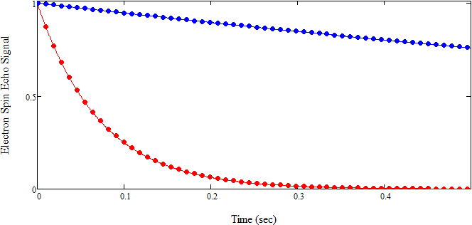
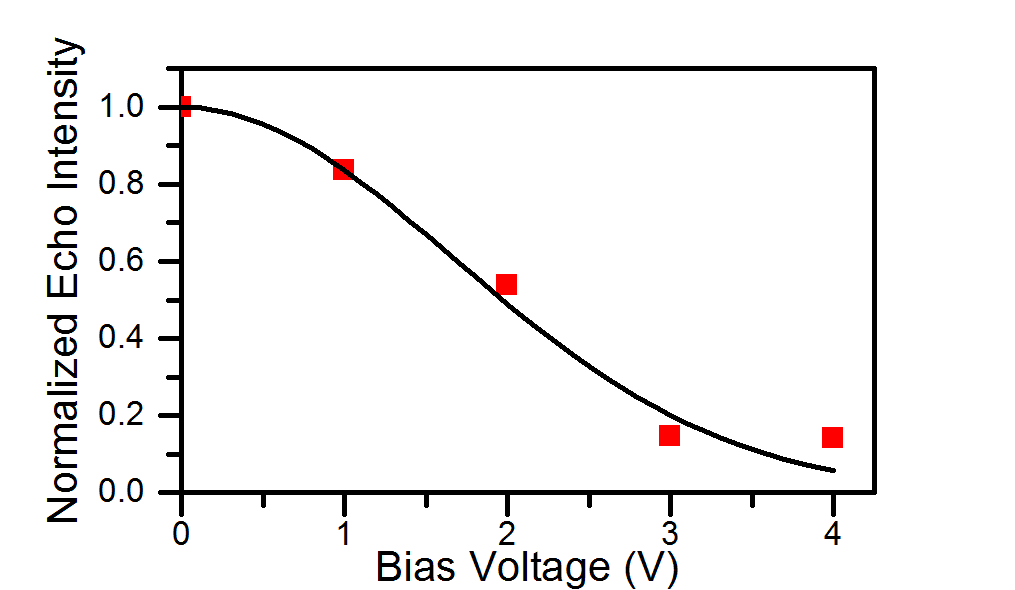
When applying unipolar electric-field pulses, in addition to the Hahn echo phase shift, we observed a rapid decrease of the ESR signal as the bias amplitude was increased. This is due to a distribution in the Stark shifts over the spin ensemble. Recovery of the echo signal when applying bipolar electric-field pulses indicate that the distribution is due to linear Stark effects. The unipolar pulse data taken with bias amplitudes up to are displayed in Fig. S2.
We model the signal loss due to line broadening from unipolar electric-field pulses by putting the Stark-induced phase shift from Eq.(3) into the model described by Eq.(2) in the main text. By assuming a Gaussian distribution of we fit to the observed decrease in echo amplitude as a function of applied bias voltage as shown in Fig. S2. We find that the strain distribution has a standard deviation of .
IV 3. Calculation of electric-field noise suppression
To quantify the effect of electric-field noise on , we have modelled the decoherence for our devices in the Bloch-Wangness-Redfield limit using reference [22] of the main text. Assuming realistic values for internal strain and assuming that the electric-field noise comes from voltage fluctuations on the gate, we plot the decays for spins both at and away from the noise suppression point.
IV.1
IV.1.1