Temperature Dependence of Joule heating in Zigzag Graphene Nanoribbon
Abstract
Using full-band electron and phonon dispersion relation, we investigate the temperature dependence of Joule heating in Zigzag Graphene Nanoribbons under high-field. At different temperatures of 300 K, 600 K, and 900 K, the Joule heating always increases linearly with time or the power is a constant. Although the scattering rates at 900 K and 600 K are 113 and 55 times higher than that of 300 K, the Joule heating power of 900 K and 600 K are just 12.6 and 6.7 timers higher than that of 300 K.
- PACS numbers
-
76.67.-n, 78.40.-q
pacs:
Valid PACS appear hereThe excellent electrical, thermal, and mechanical properties of graphene nanoribbons hold many promising application in electronics Geim and Novoselov (2007); Han et al. (2007); Li et al. (2008); Geim (2009); Schwierz (2010). To design energy-efficient circuits and energy-conversion systems, it is of great importance to understand energy dissipation and transport in nanoscale structures. The dissipated electric power can then raise the operating temperature to a point where thermal management becomes critical. The high current-carrying capacity is also critical for reliability, as many research works demonstrate Joule heating as the main failure mechanism Wang et al. (2008); Liao et al. (2011); Murali et al. (2009).
The straightforward measurement method is to probe limiting current density by measuring I-V until devices break down. For solution-deposited GNRs of sub-10nm width Wang et al. (2008), the limiting current density is around . As bilayer graphene was used here, the current density is equivalent to . Another experiment based on solution deposited GNRs was carried out by Liao et. al. Liao et al. (2011), they found that the maximum current density is limited by self-heating. For GNRs with 15 nm wide, the current can reach . These values are obtained for GNRs without perfect edge due to possibly mixed edge shape and dangling bonds. Thus, edge scattering plays an important role in narrow GNRs. More promising results can be obtained with better fabrication methods available. For exfoliated GNRs up to five layers, Murali et. al. Murali et al. (2009) demonstrated a limit current density of 1.2 - 2.8. And the breakdown current density is found to have a reciprocal relationship to GNR resistivity, which fit points to Joule heating as the likely mechanism of breakdown.
To assess the intrinsic current carrying ability of GNRs, however, theoretical analysis must be sought to study the carrier transport and scattering mechanism in GNRs. In this study, we investigate the temperature dependence of Joule heating in Zigzag Graphene Nanoribbons under high-field, using Ensemble Monte Carlo simulations with full-band electron and phonon dispersion relation.
Within the formulation of tight-binding method, the energy bands of ZGNR with N dimers can be solved analytically as Wakabayashi et al. (2010),
| (1) |
where and in the longitudinal wave number. The sub band is labelled by the quantization parameter in the transveral direction, which is determined by,
| (2) |
The reason is that the energy should always be a real number, thus the imaginary part should be zero. For ZGNR with even dimers, each sub band can be shown to have a parity of even or odd, which is identical to the even or odd of [ref: APL paper]. For ZGNR with 10 dimers, the band structure is shown in Fig. 1.
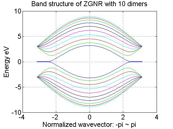
The band gap in Fig. 1 is 0, which is intrinsic to the tight-binding model and is always 0 for ZGNRs with any dimers. Based on these results, ZGNRs are said to be metallic and proposed as a promising replacement for conventional interconnects in electronics Hod et al. (2007); Xu et al. (2009); Naeemi and Meindl (2009). But according to first principle calculations Son et al. (2006), ZGNRs have a band gap depending on the width of nanoribbon and the magnitude is on the order of 0.2 eV. However, the Fermi level of ZGNR can be easily lifted to overcome this band gap. In this study, the Fermi level is set at the bottom of conduction band and all valence bands are fully occupied. Thus, the conduction bands obtained by tight-binding method works well as the first approximation.
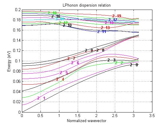
The phonon dispersion relation of ZGNR is obtained by Force Constant Methods Saito et al. (1998), as shown in Fig. 2. Similar to the vibration of membranes with two free edges, the modal shapes have the forms of sine functions (odd) or cosine functions (even). Approximately, the wave length and wave number of mode can be expressed as
| (3) |
where is the width of ZGNR and is the number of nodes in the width direction. The modal shape and parity were also verified by first principle calculations Yamada et al. (2008); Gillen et al. (2009). Here, we only consider the longitudinal modes as their deformation potential are quite big than those of transverse mode and out-of-plane modes Obradovic et al. (2006).
Based on the preceding discussion, both electron and phonon have the parity. Due to geometricall mirror symmetry for lattice of ZGNR with even dimers, the parity should be conserved in the electron and phonon interaction process [cite APL]. Other than this, the electron can be scattered by a phonon to any sub bands without violating parity conservation, this the so called transverse momentum conservation uncertainty Betti et al. (2011). As usual, the selection rule also includes the conservation of energy and the conservation of longitudinal momentum. By Fermi’s Golden Rule, the scattering rates can be calculated as
| (4) |
where is the matrix element for an electron gets scattered by a specific phonon mode from intial state to final state .
For the three-particle process here, the parity conservation is equivalent to:
| (5) |
where represents either a phonon or electron. In other words, for the scattering process with electron jumping from even state to even state or odd state to odd state, the parity of the involved phonon can only be even. Similarly, only odd phonons can scatter electrons from even state to odd state or odd state to even state.
Therefore, the matrix element is always even about the dimer index and can be written as
| (6) |
Here, , , and are the number of unit cell in the system, mass of carbon atom, and number of phonons respectively; the Kronecker delta describes the conservation of momentum in the longitudinal direction; is the magnitude of electron wave and is normalized by ; similarly, and are magnitude and normalization constant for even phonons, while and are magnitude and normalization constant for odd phonons; the deformation potential for optical phonon is eV/cm Fang et al. (2008), and the deformation potential for acoustic phonon is 16 eV Pennington et al. (2007).
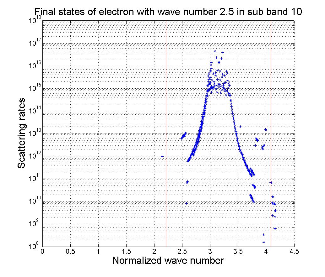
The scattering rates for ZGNR with 10 dimers are demonstated in Fig. 3. Since the Fermi level is set at the bottom of conduction band, most electron resides at the lowest conduction band (electron sub band 10), only the scattering rates of sub band 9 and sub band 10 are presented. Generally, the scattering rates at room temperature (300 K) is orders higher than the values for Carbon Nanotube. One reason is that the absence of the periodical boundary condition in the restricted direction of ZGNR, which removes the selection rule of subband number conservation. Therefore, each electron can interact with all 10 branches of phonons and justifies the difference between ZGNR and CNT.
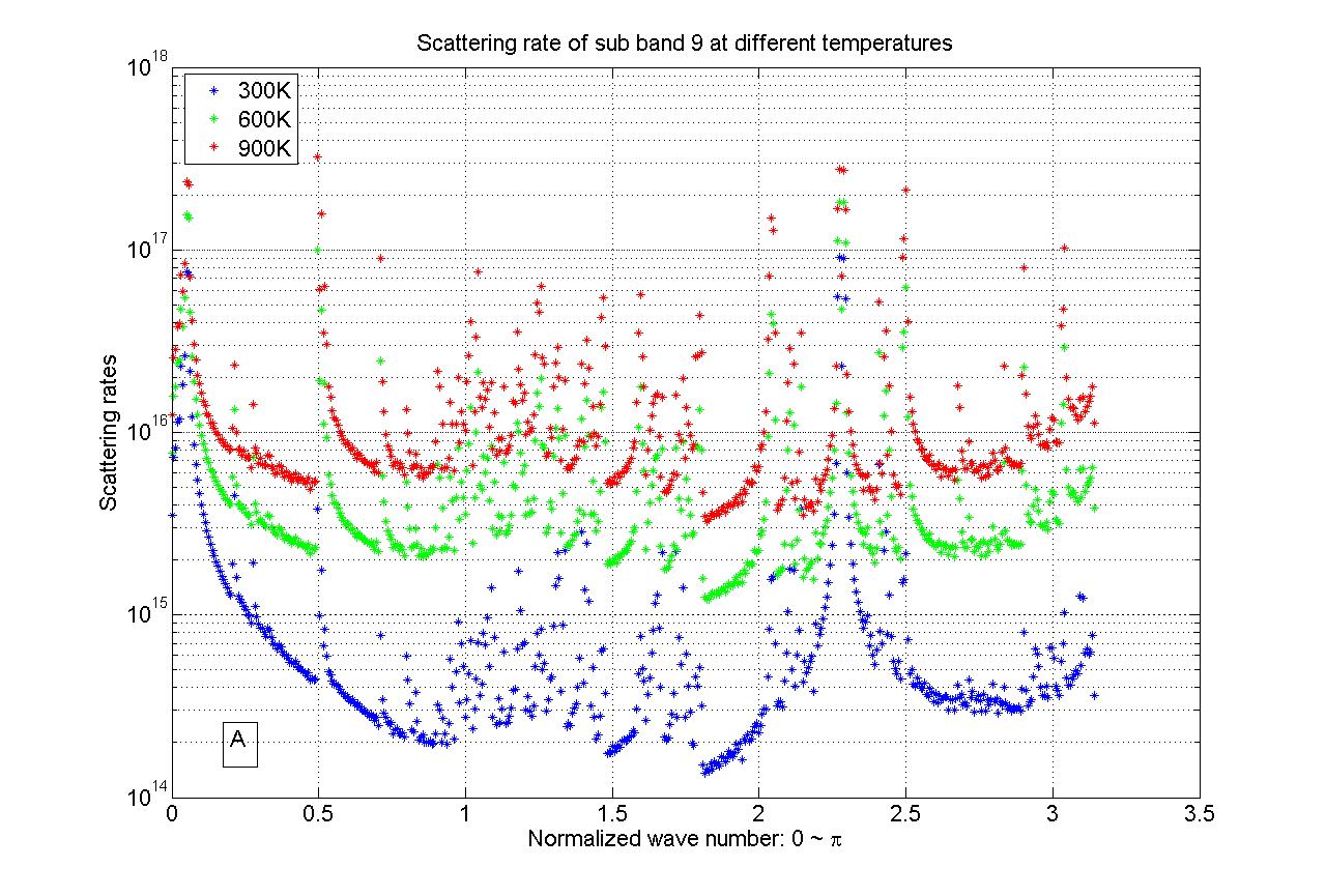
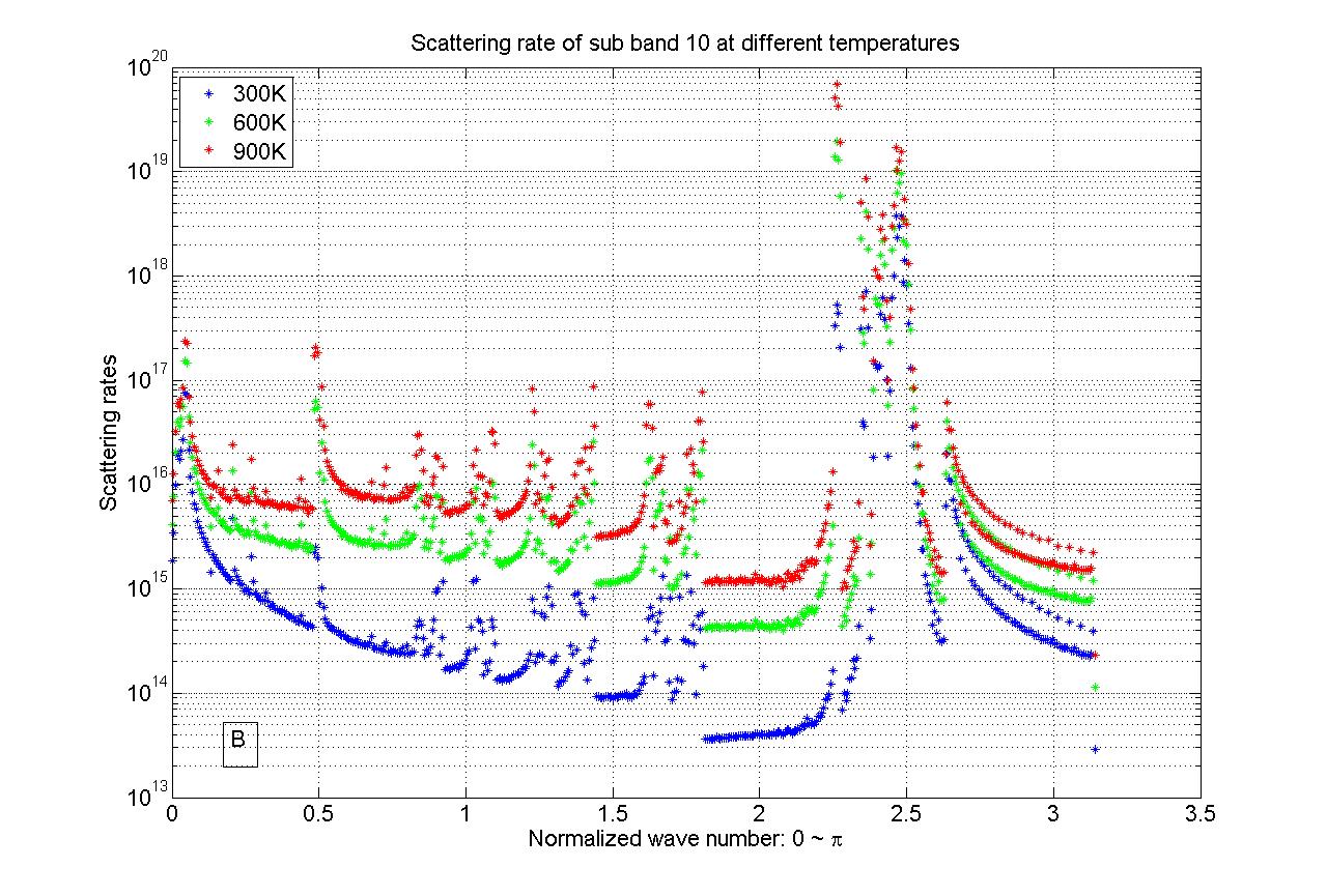
Another reason for the much higher scattering rates is due to the formulation. According to Betti et. al. Betti et al. (2011), the term related to mass in scattering rates is , where is the width of nanoribbon and is the 2D graphene mass density. However, the expression for this term is with as the unit length of ZGNR. Obviously both of them has a dimension of length density. But in our formulation the term is a constant while in the formualtion of Betti et. al. it denpends on the width . For wider nanoribbons could be tens of and result in a scattering rates tenth of our results.
As shown in Fig. 3, scattering rates at the same temperature are quite different even for different electron states (with different wave number) of the same sub band. To describe the free flight time between scattering, however, we need to assume a nominal scattering rate for all different electron states Lundstrom (2009). The parameter is very important as it determines the size of reasonable time step in the Ensemble Monte Carlo (EMC), which in turns determines the efficiency of EMC simulation. According to Fig. 3, the highest scattering rates for electrons in sub band 10 are on the order of . Therefore, the time step should be set on the order of s, which is unreasonable small. Another problem is that the highest and lowest scattering rates for sub band 10 are of 5 oders different even at the same temperatures. In the scattering mechanisms scattering process, this implies that the self scattering probability is after the free flight. In other words, the physical probability for electron get scattered is only 0.001%, which makes the simulation extremely inefficient.
We should make two observations here. First, the electron states with highest scattering rates are those with wave numbers around 2.5 (normalized by 1/a). In tight-binding model for ZGNR with 10 dimers, all electron states in sub band 10 with wave numbers larger than 2.13 are the almost flat edge states with extremely density of state. According to first principle calculations, the segment of band 10 corresponding to edge states is not flat. Second, the detailed inspection of the final states for all electrons in this range shown that, the involved phonons have almost zero energy. As we are only interested in the energy transfer between phonons and electrons, the contribution of these scattering events is very week. Therefore, we can normalize these scattering rates to to expedite our simulation.
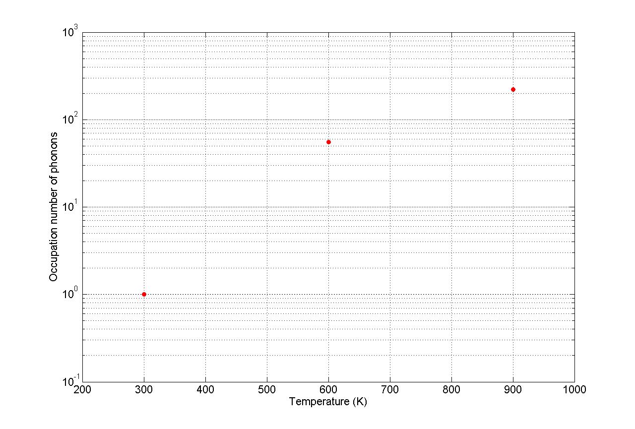
In the formulation of scattering rates, the temperature denpendence only comes from the phonon occupation number . As one kind of Bosons, of phonons follow the Bose-Einstein distribution,
| (7) |
wherer is the temperature. Take optical phonons as an example, whose energy can be assumed as constant with the value of 0.2 eV. The occupation numbers at different temperature (300 K, 600 K, and 900 K) are shown in Fig. 5. The occupation number at 600 K is about 55 times higher than the occupation number at 300 k, while that at 900 K is 113 times higher. This explains the magnitudes of scattering rates at different temperatures.
In the EMC simulations, the first Brillouin zone for both electron and phonon is discretized by 1000 points. According the quantization scheme of Bloch’s Theorem, this implies that we are studying a system of the 1000 unit cells long in the real space. For a specific temperature and Fermi level, the calculated electron occupation number in reciprocal space is equivalent to electrons per unit cell in real space. Correspondingly, the linear electron density in real space is . With the Fermi level set as 0, the occupation number of 300 K, 600 K, and 900 K in reciprocal space are 54, 59, and 63 respectively. According to the preceding discussion of renormalized scattering rates, the time step for temperature at 300 K, 600 K, and 900K are set as fs, fs, and fs respectively. Each simulation runs for fs. And the high electrical field in this study is set as 20 kV/cm.
Quantum mechanically, Joule heating power is the energy transfered from electrons to phonons and can be calculated as Gautreau et al. (2012),
| (8) |
where is the energy transferred during the scattering event from an initial state to a final state by scattering mechanism and the corresponding scattering rate is ; is the occupation probability of the state , while is the probability that state is unoccupied.
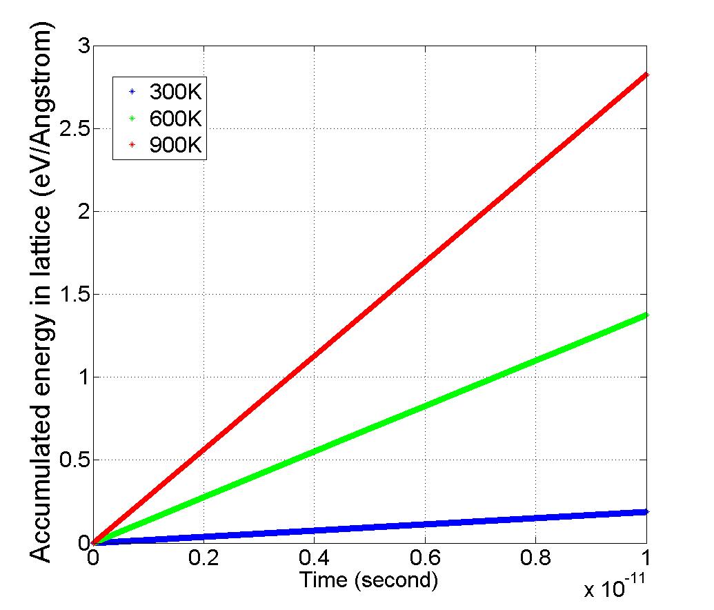
The results of EMC simulations are demonstrated in Fig. 6. It shows that the accumulated energy transfered from electrons to lattice at different temperatures always increases linearly with time. Or the Joule heating power is a constant. Although the scattering rates at 900 K and 600 K are 113 and 55 times higher than that of 300 K, the Joule heating power of 900 K and 600 K are just 12.6 and 6.7 timers higher than that of 300 K.
We would like to recognize the contribution of Dr. Xuedong Hu of the Physics Department at the University at Buffalo for our insightful discussions. We also gratefully acknowledge the financial support received from the US Navy Office of Naval Research Advanced Electrical Power Systems program, under the direction of Dr. Peter Chu.
References
- Geim and Novoselov (2007) A. K. Geim and K. S. Novoselov, Nature materials 6, 183 (2007).
- Han et al. (2007) M. Y. Han, B. Özyilmaz, Y. Zhang, and P. Kim, Physical review letters 98, 206805 (2007).
- Li et al. (2008) X. Li, X. Wang, L. Zhang, S. Lee, and H. Dai, Science 319, 1229 (2008).
- Geim (2009) A. K. Geim, science 324, 1530 (2009).
- Schwierz (2010) F. Schwierz, Nature nanotechnology 5, 487 (2010).
- Wang et al. (2008) X. Wang, Y. Ouyang, X. Li, H. Wang, J. Guo, and H. Dai, Phys. Rev. Lett. 100, 206803 (2008).
- Liao et al. (2011) A. D. Liao, J. Z. Wu, X. Wang, K. Tahy, D. Jena, H. Dai, and E. Pop, Phys. Rev. Lett. 106, 256801 (2011).
- Murali et al. (2009) R. Murali, Y. Yang, K. Brenner, T. Beck, and J. D. Meindl, Applied Physics Letters 94, 243114 (2009).
- Wakabayashi et al. (2010) K. Wakabayashi, K. Sasaki, T. Nakanishi, and T. Enoki, Science and Technology of Advanced Materials 11, 054504 (2010).
- Hod et al. (2007) O. Hod, V. Barone, J. E. Peralta, and G. E. Scuseria, Nano letters 7, 2295 (2007).
- Xu et al. (2009) C. Xu, H. Li, and K. Banerjee, Electron Devices, IEEE Transactions on 56, 1567 (2009).
- Naeemi and Meindl (2009) A. Naeemi and J. D. Meindl, Electron Devices, IEEE Transactions on 56, 1822 (2009).
- Son et al. (2006) Y.-W. Son, M. L. Cohen, and S. G. Louie, Nature 444, 347 (2006).
- Saito et al. (1998) R. Saito, G. Dresselhaus, and S. Dresselhaus, Physical Properties of Carbon Nanotubes (Imperial College Press, 1998).
- Yamada et al. (2008) M. Yamada, Y. Yamakita, and K. Ohno, Phys. Rev. B 77, 054302 (2008).
- Gillen et al. (2009) R. Gillen, M. Mohr, C. Thomsen, and J. Maultzsch, Phys. Rev. B 80, 155418 (2009).
- Obradovic et al. (2006) B. Obradovic, R. Kotlyar, F. Heinz, P. Matagne, T. Rakshit, M. D. Giles, M. A. Stettler, and D. E. Nikonov, Applied Physics Letters 88, 142102 (2006).
- Betti et al. (2011) A. Betti, G. Fiori, and G. Iannaccone, Applied Physics Letters 98, 212111 (2011).
- Fang et al. (2008) T. Fang, A. Konar, H. Xing, and D. Jena, Phys. Rev. B 78, 205403 (2008).
- Pennington et al. (2007) G. Pennington, N. Goldsman, A. Akturk, and A. E. Wickenden, Applied Physics Letters 90, 062110 (2007).
- Lundstrom (2009) M. Lundstrom, Fundamentals of Carrier Transport (Cambridge University Press, 2009).
- Gautreau et al. (2012) P. Gautreau, T. Ragab, and C. Basaran, Journal of Applied Physics 112, 103527 (2012).