Graphene-on-silicon near-field thermophotovoltaic cell
Abstract
A graphene layer on top of a dielectric can dramatically influence ability of the material to radiative heat transfer. This property of graphene is used to improve the performance and reduce costs of near-field thermophotovoltaic cells. Instead of low bandgap semiconductors it is proposed to use graphene-on-silicon Schottky photovoltaic cells. One layer of graphene absorbs around 90% of incoming radiation and increases the heat transfer. This is due to excitation of plasmons in graphene, which are automatically tuned in resonance with the emitted light in the mid infrared range. The absorbed radiation excites electron-hole pairs in graphene, which are separated by the surface field induced by the Schottky barrier. For a quasi-monochromatic source the generated power is one order of magnitude larger and efficiency is on the same level as for semiconductor photovoltaic cells.
pacs:
44.40.+a, 78.67.-n, 73.50.Pz, 88.40.-jI Introduction
Thermophotovoltaic (TPV) generators convert radiation emitted by a heated body into electricity Cou01 . In these devices a hot emitter radiates the electromagnetic energy that is absorbed by a cold photovoltaic (PV) cell (collector). In the solar TPV generators Len14 solar light is absorbed and then re-emitted as thermal radiation in a spectrally selective way. Any other heat source also can be used for transformation into electricity: wasted industrial heat, the heat from car engines, computer chips etc. Bas09 ; Bos12 . TPV systems are expected to be quiet, modular, safe, low-maintenance, and pollution-free Cou01 .
The main challenge is to increase both efficiency and output electric power of the devices. The power is restricted by the emissivity of the black body. This restriction, however, is not applicable when the bodies are separated by a distance much smaller than the thermal wavelength Pol71 . In this near-field range the radiative heat transfer (RHT) can be increased by orders of magnitude Pen99 ; Par02 ; Mul02 . Significant enhancement of the RHT in the near-field was demonstrated experimentally Har69 ; Kit05 ; Hu_08 ; Nar08 ; She09 ; Rou09 . The highest efficiency is reached when the emitter is a nearly monochromatic source of radiation with the photon energy slightly larger than the band gap of the PV cell Lar06 . On the other hand, the strongest enhancement is realized as the resonance energy exchange when both the emitter and collector support surface modes such as plasmon or phonon-polaritons matching each other Jou05 ; Vol07 . The absorption of light by semiconductor PV cells does not have resonance character and cannot support high RHT. Moreover, TPV generators have to use narrow band semiconductors, which are much more expensive than silicon. In this paper we explain how graphene could help to resolve these issues.
Graphene can add new functionalities to materials that do not have surface modes in the mid infrared (IR) range Sve12 . This is because graphene supports plasmons with the frequency that is varied with the wave number, coupling constant, and Fermi level Jab09 . The plasmon frequency in graphene is automatically tuned with the frequency of the surface mode in the opposing body resulting in a significant increase of the RHT Sve12 ; Ili12b . This prediction was also confirmed experimentally Zwo12 .
Here we propose to use graphene-on-silicon (g/Si) Schottky photodiode as a PV cell. In such a generator the emitted radiation is resonantly absorbed in graphene where it excites electrons able to overcome the Schottky barrier, there is no p-n junction and related optical losses in the low price Si substrate, there is no problem to couple the evanescent radiation to electrons in graphene, and the device has a simple structure. The silicon substrate is transparent in the wavelength range providing the optimal conditions for the RHT Sve12 .
The g/Si Schottky photodiodes were already applied for solar cells Li_10 ; Ye_12 ; Mia12 , where the visible light generated electron-hole pairs in Si separated by the surface field. The photodiode presented in Wan13 absorbs mid IR light in the graphene layer and the Schottky barrier separates electrons and holes. The responsivity of the device was estimated as at least 0.13 A/W.
Application of graphene to enhance performance of the near-field TPV generators was already discussed. A free-standing graphene emitter was considered in combination with the low bandgap (0.17 eV) InSb photovoltaic cell Ili12a . For this device there is no resonance energy exchange between graphene and the semiconductor. A PV cell consisting of InSb substrate covered with graphene was discussed in Mes13 , where hexagonal Boron Nitride (hBN) was used as the emitter. In this device the RHT is enhanced due to the resonance tuning but most of the photons are absorbed in graphene without generation of photoelectrons.
II Heat transfer
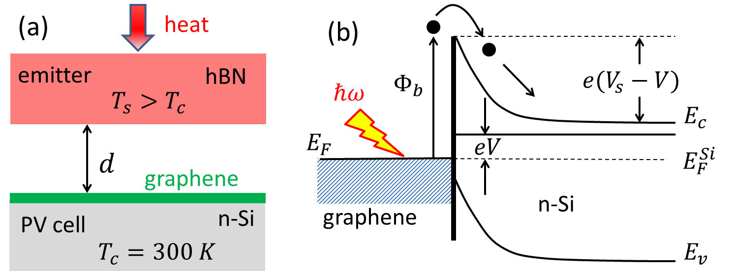
We consider graphene-on-silicon Schottky junction in combination with the hBN emitter that gives quasi-monochromatic radiation at 0.195 eV (see Fig. 1(a)). This specific emitter is not the point of interest as long as the photoelectrons can overcome the Schottky barrier. Moreover, a wider range of emitted frequencies is preferable. It is assumed that the bottom of the PV cell is kept at room temperature K but the emitter temperature can vary.
The energy scheme of the photodiode is shown in Fig. 1(b). Silicon of n-type is shown but p-type also can be used. Infrared radiation from the emitter is absorbed in graphene providing hot electrons that are able to overcome the Schottky barrier , where is the Fermi level in graphene and is the electron affinity in silicon. The surface barrier from the Si side is and the forward bias applied to the diode is . The edges of the conduction and valence bands are and , respectively, the Fermi level in Si is .
In contrast with the ordinary PV cells Si is transparent for the emitted radiation. The Fermi level in pristine graphene is eV Yan12b but it can be adjusted by chemical doping of graphene in a wide range Jeo10 ; Yi_11 ; Shi10 . The barrier height has to be eV or lower if hBN emitter is used. This height can be reached for n-doping in graphene with the relative Fermi level eV counted from the Dirac point. The band bending in Si is defined by the surface potential .
The photocurrent is generated by photons with the energy absorbed in the graphene layer. The radiation of emitter absorbed in graphene can be calculated as
| (1) |
Here is the heat flux from the emitter to the collector taken in the gap just above the graphene layer. This flux is calculated as the -component of the averaged Pointing vector induced by the fluctuations in the emitter. The flux is calculated in a similar way but just below the graphene layer. These fluxes can be presented in the form
| (2) |
where is the Bose factor (the Boltzmann constant here is ). The evanescent spectral function is
| (3) |
Here and are the reflection coefficients of the source and collector, respectively, which are functions of and the wave vector q parallel to the plates. The result for is well known Pol71 ; Mul02 ; Jou05 ; Vol07 but the expression for has to be calculated. It can be done using the standard approach of fluctuational electrodynamics. Skipping the details, the final expression for the spectral function is
| (4) |
where is the dielectric function of graphene and is the average dielectric constant of the media above and below the graphene layer.
Graphene is responsible for the energy exchange in the system. Without graphene on top of silicon the heat transfer is negligible because Si is transparent for the emitteed radiation. It is known that the effect of graphene can be evaluated with a good precision () in the non-retarded limit Gom09 ; Sve11 ; Sve12 , where only p-polarized evanescent fluctuations contribute to the momentum or energy exchange between parallel plates separated by a submicrometer gap. Therefore, in Eqs. (2)-(4) it is sufficient to take into account only the contribution of p-polarized evanescent waves.
In order to calculate the total energy exchange between bodies we have to include the heat flux going to the emitter and originating from fluctuations in the collector. Normally it can be done by the substitute in Eq. (2)
| (5) |
because in the thermal equilibrium the total RHT has to be zero Pol71 . However, the procedure is different if the collector is used as a PV element. As for semiconductors Wur82 ; Luq03 the potential difference results in non-thermal photons that have non-zero chemical potential but still can be described by the collector temperature . This is true for photons with the energy above the Schottky barrier ; the photons with smaller energies have . In this case the thermal factor is defined as
| (6) |
where we have to understand as a discontinuous function of
| (7) |
The final result for the radiative power per unit area is
| (8) |
It is similar to the expression used in Ili12a ; Mes13 . The difference is that in our case the collector emits radiation with due to presence of graphene, while for a semiconductor PV cell with the bandgap the adopted approximation is that the radiation with is not emitted. The radiative power absorbed in the graphene layer can be calculated from (8) with the substitute .
III Generated power
Let us assume first that each photon with the energy above which is absorbed in graphene produces one electron in the conduction band of Si. The actual responsivity of the photodiode will be discussed later. In this case the photocurrent generated in the cell Lar06 is
| (9) |
It is proportional to the number of photons with the energy above absorbed in graphene. The generated electrical power and efficiency of the cell are defined as
| (10) |
where is similar to that used in Refs. Ili12a ; Mes13 . Note that does not include the efficiency of heating of the emitter and the efficiency of light transformation by the photodiode. The electric power is zero for corresponding to the short circuit and for corresponding to the open circuit voltage. The maximal power is realized somewhere in between these values.
The dielectric function of the emitter is described by the Drude-Lorentz model
| (11) |
with the parameters of hBN from Nar03 , eV, eV, and eV. The reflection coefficient of the emitter (p-polarization, non-retarded) has a surface phonon-polariton resonance at 0.195 eV.
The reflection coefficient of the collector can be presented in the form
| (12) |
where is practically a constant for Si in mid IR and is the dielectric function of graphene. In the limit of small relaxation frequency the latter can be presented in the form
| (13) |
where is the coupling constant and is the Fermi velocity in graphene. Equation (13) can be applied in the range ; finite can be accounted with the substitute and some not essential modification of (see Sve12 ; Ili12b for details).
The spatial dispersion of is an important property. It results in the plasmon frequency that depends on even in the non-retarded limit:
| (14) |
This dependence means that for a body covered with graphene one can always find a value of that gives the plasmon resonance matching the surface mode in the opposite body. When the substrate permittivity is large, graphene gives only small correction to and there will be no significant increase in RHT. For silicon it is rather large but even a thin native oxide ( nm) on Si influences the reflection coefficient. We take this oxide into account in our calculations and use the graphene relaxation frequency meV ( rad/s).
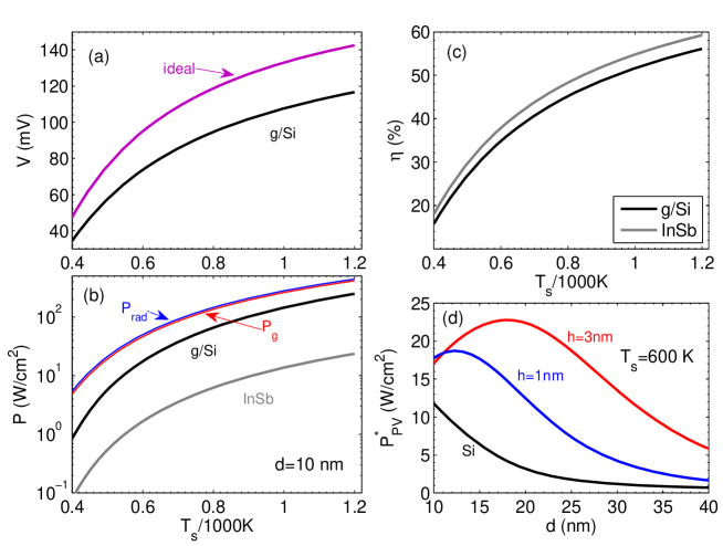
The results are shown in Fig. 2. First, using Eq. (10) the output power was maximized by varying the operating voltage of the cell . The theoretical limit of this voltage and the value found from the maximization of at nm are shown in Fig. 2a as functions of the emitter temperature. The optimal value of varies only slightly with the distance. The net radiative power and the power absorbed in graphene are shown in Fig. 2b. The curves are nearly coincide because about 90% of incoming radiation is absorbed in graphene. This exceptional phenomena is the result of plasmon excitation in resonance with the radiation of the emitter. The output power of the cell is also presented in Fig. 2b. For comparison for the InSb PV cell is shown too, which is one order of magnitude smaller. The efficiency for g/Si cell shown in Fig. 2c is somewhat smaller than that for the InSb cell. It happens because 90% of the light incoming on the g/Si cell generates photocarriers, while it was assumed that 100% of the light generates carriers in the semiconductor cell. The latter, of course, is not true because to contribute to the photocurrent the electron-hole pairs has to reach the depletion layer before recombination Par08 ; Fra11 . We can conclude that the TPV element with the graphene-on-Si Schottky PV cell can outperform semiconductor PV cells if the responsivity of the Schottky photodiode will be comparable with that of low bandgap semiconductors.
The dependence of the scaled output powers on the distance is shown in Fig. 2d for three different thicknesses of the SiO2 layer on Si. All the curves are presented for K. At the maximum the frequency of plasmon (14) matches the resonance in the emitter eV at . Deviation from this relation in any direction will result in decrease of the scaled power. Graphene on a thin silicon oxide film corresponds to some intermediate situation between pure Si and pure SiO2.
For low barrier height the surface electric field at high becomes too small for the carriers separation (the same problem exists for low bandgap semiconductors). It is therefore interesting to analyze the behavior of the g/Si cell for different barrier heights. To perform this analysis we model the emitter with the dielectric function similar to (11) but with the parameters , which are close to those for hBN. The resonance frequency of the reflection coefficient
| (15) |
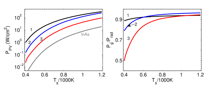
is the varied parameter, where is the static permittivity of the emitter. It is assumed that the barrier height is somewhat smaller than . Some results are shown in Fig. 3. The left panel shows that the output power is smaller for higher barrier at low but becomes comparable or even larger at high as the curves 1 and 2 demonstrate. However, when the barrier is too high becomes smaller at all temperatures. The reason is that the value of the momentum in (14) for which becomes significantly larger than . It reduces the radiative power due to the factor and results in the decrease of . The output power produced by InAs PV cell with the bandgap 0.36 eV is shown for comparison in the same panel. The right panel shows the fraction of the radiative power absorbed in graphene for different barrier heights. This fraction is always large especially at high . It is somewhat smaller at low temperatures and high barriers.
Dependence on the barrier height demonstrates that g/Si PV cell is able to support plasmons in the mid IR range where it is superior over the semiconductor PV cells. At shorter wavelengths m the radiative heat exchange is significantly reduced and the g/Si cell loses its advantages.
IV Discussion
Up to now we assumed that the photodetector is perfect. The typical responsivity of low bandgap semiconductors is 1 A/W. It is still larger than the reported value 0.13 A/W Wan13 for the g/Si Schottky photodiode. However, the main problem of graphene-based photodetectors is the coupling of light with graphene. For incoming propagating waves absorption in graphene is small . To increase the responsivity one has to couple light with sophisticated optical structures (see Wan13 and references therein). These structures inevitably add losses reducing the effective responsivity. Additionally, the graphene-Si junction was not optimized. The configuration used in our scheme does not suffer from the coupling problem because the heat transfer is realized via the evanescent waves, for which we have found that 90% of incoming radiation is absorbed in a single graphene layer. Therefore, the responsivity for our configuration can be increased well above 0.13 A/W.
At this moment control of the gap in a few tens of nanometers between parallel plates is a very challenging problem. However, progress in this direction is fast. The distances 30-60 nm are already explored for RHT experimentally Zwo12 ; She12 ; Shi13 in the sphere-plate configuration. In the parallel plates configuration the heat transfer was investigated at distances up to 1 m Ott11 ; Kra12 . Large parallel plates separated by a distance of 100 nm or smaller is also an important problem for many micromechanical applications and it is actively investigated Sye13 ; Woo13 . For this reason we hope that our proposition can be reality in the near future.
V Conclusions
We considered the near-field TPV element having as a PV cell graphene-on-silicon Schottky photodiode. Due to presence of graphene this PV cell has resonant heat exchange with the emitter; a single layer of graphene absorbs 90% of incoming radiation that can be efficiently transformed to photocurrent. Already for quasi-monochromatic emitter the device demonstrates well advanced characteristics.
References
- (1) T. J. Coutts, An overview of thermophotovoltaic generation of electricity, Sol. Energy Mater. Sol. Cells 66, 443 (2001).
- (2) A. Lenert, D. M. Bierman, Y. Nam, W. R. Chan, I. Celanovic, M. Soljačić, and E. N. Wang, A nanophotonic solar thermophotovoltaic device, Nature Nano. 9, 126 (2014).
- (3) S. Basu, Z. M. Zhang and C. J. Fu, Review of near-field thermal radiation and its application to energy conversion, Int. J. Energy Res. 33, 1203 (2009).
- (4) M. Bosi, C. Ferrari, M. Franceso, M. Pinelli, P. R. Spina, and M. Venturini, Thermophotovoltaic generation: A state of the art review, in Proceedings of the International Conference on Efficiency, Cost, Optimization, Simulation and Envinromental Impact of Energy Systems, 2012, edited by U. Desideri, G. Manfrida, E. Sciubba (Firenze University, Perugia, 2012), p. 258.
- (5) D. Polder and M. Van Hove, Theory of radiative heat transfer between closely spaced bodies, Phys. Rev. B 4, 3303 (1971).
- (6) J. B. Pendry, Radiative exchange of heat between nanostructures, J. Phys.: Condens. Matter 11, 6621 (1999).
- (7) C. H. Park, H. A. Haus, and M. S. Weinberg, Proximity-enhanced thermal radiation, J. Phys. D 35, 2857 (2002).
- (8) J.-P. Mulet, K. Joulain, R. Carminati, and J.-J. Greffet, Enhanced radiative heat transfer at nanometric distances, 6, 209 (2002).
- (9) C. Hargreaves, Anomalous radiative transfer between closely-spaced bodies, Phys. Lett. A 30, 491 (1969).
- (10) A. Kittel, W. Müller-Hirsch, J. Parisi, S.-A. Biehs, D. Reddig, and M. Holthaus, Near-field heat transfer in a scanning thermal microscope, Phys. Rev. Lett. 95, 224301 (2005).
- (11) L. Hu, A. Narayanaswamy, X. Chen, and G. Chen, Near-field thermal radiation between two closely spaced glass plates exceeding Planck s blackbody radiation law, Appl. Phys. Lett. 92, 133106 (2008).
- (12) A. Narayanaswamy, S. Shen, and G. Chen, Near-field radiative heat transfer between a sphere and a substrate, Phys. Rev. B 78, 115303 (2008).
- (13) S. Shen, A. Narayanaswamy, and G. Chen, Surface phonon polaritons mediated energy transfer between nanoscale gaps, Nano Lett. 9, 2909 (2009).
- (14) E. Rousseau, A. Siria, G. Jourdan, F. Comin, J. Chevrier, and J.-J. Greffet, Radiative heat transfer at the nanoscale , Nature. Photon. 3, 514 (2009).
- (15) M. Laroche, R. Carminati, and J.-J. Greffet, Near-field thermophotovoltaic energy conversion, J. Appl. Phys. 100, 063704 (2006).
- (16) K. Joulain, J.-P.Mulet, F.Marquier, R. Carminati, and J.-J. Greffet, Surface electromagnetic waves thermally excited: Radiative heat transfer, coherence properties and Casimir forces revisited in the near field, Surf. Sci. Rep. 57, 59 (2005).
- (17) A. I. Volokitin and B. N. J. Persson, Near-field radiative heat transfer and noncontact friction, Rev. Mod. Phys. 79, 1291 (2007).
- (18) V. B. Svetovoy, P. J. van Zwol, and J. Chevrier, Plasmon enhanced near-field radiative heat transfer for graphene covered dielectrics, Phys. Rev. B 85, 155418 (2012).
- (19) M. Jablan, H. Buljan, and M. Soljačić, Plasmonics in graphene at infrared frequencies, Phys. Rev. B 80, 245435 (2009).
- (20) O. Ilic, M. Jablan, J. D. Joannopoulos, I. Celanović, H. Buljan and M. Soljačić, Near-field thermal radiation transfer controlled by plasmons in graphene, Phys. Rev. B 85, 155422 (2012).
- (21) P. J. van Zwol, S. Thiele, C. Berger, W. A. de Heer, and J. Chevrier, Nanoscale radiative heat flow due to surface plasmons in graphene and doped silicon, Phys. Rev. Lett. 109 264301 (2012).
- (22) X. Li, H. Zhu, K. Wang, A. Cao, J. Wei, C. Li, Y. Jia, Z. Li, X. Li, and D. Wu , Graphene-on-silicon Schottky junction solar cells, Adv. Mater. 22, 2743 (2010).
- (23) Y. Ye and L. Dai, Graphene-based Schottky junction solar cells, J. Mater. Chem. 22, 24224 (2012).
- (24) X. Miao, S. Tongay, M. K. Petterson, K. Berke, A. G. Rinzler, B. R. Appleton, and A. F. Hebard, High efficiency graphene solar cells by chemical doping, Nano Lett. 12, 2745 (2012).
- (25) X. Wang, Z. Cheng, K. Xu, H.-K. Tsang, and J.-B. Xu, High-responsivity graphene/silicon-heterostructure waveguide photodetectors, Nature Photon. 7, 888 (2013).
- (26) O. Ilic, M. Jablan, J. D. Joannopoulos, I. Celanovic and M. Soljačić, Overcoming the black body limit in plasmonic and graphene near-field thermophotovoltaic systems, Opt. Express 20, A366 (2012).
- (27) R. Messina and P. Ben-Abdallah, Graphene-based photovoltaic cells for near-field thermal energy conversion, Sci. Rep. 3, 1383 (2013).
- (28) R. Yan, Q. Zhang, W. Li, I. Calizo, T. Shen, C. A. Richter, A. R. Hight-Walker, X. Liang, A. Seabaugh, D. Jena, H. G. Xing, D. J. Gundlach, and N. V. Nguyen, Determination of graphene work function and graphene-insulator-semiconductor band alignment by internal photoemission spectroscopy, Appl. Phys. Lett. 101, 022105 (2012).
- (29) H. K. Jeong, K.-J. Kim, S. M. Kim and Y. H. Lee, Modification of the electronic structures of graphene by viologen Original, Chem. Phys. Lett. 498, 168 (2010).
- (30) Y. Yi, W. M. Choi, Y. H. Kim, J. W. Kim and S. J. Kang, Effective work function lowering of multilayer graphene films by subnanometer thick AlOx overlayers, Appl. Phys. Lett. 98, 013505 (2011).
- (31) Y. Shi, K. K. Kim, A. Reina, M. Hofmann, L.-J. Li and J. Kong, Work function engineering of graphene electrode via chemical doping, ACS Nano 4, 2689 (2010).
- (32) G. Gómez-Santos, Thermal van der Waals interaction between graphene layers, Phys. Rev. B 80, 245424 (2009).
- (33) V. B. Svetovoy, Z. Moktadir, M. C. Elwenspoek, and H. Mizuta, Tailoring the thermal Casimir force with graphene, Europhys. Lett. 96, 14006 (2011).
- (34) P. Würfel, The chemical potential of radiation, J. Phys. C 15, 3967 (1982).
- (35) A. Luque and A. Martí, in Handbook of Photovoltaic Science and Engineering. Edited by A. Luque and S. Hegedus (John Wiley & Sons, 2003).
- (36) A. Narayanaswamy and G. Chen, Surface modes for near field thermophotovoltaics, Appl. Phys. Lett. 82, 3544 (2003).
- (37) K. Park, S. Basu, W.P. King, and Z.M. Zhang, Performance analysis of near-field thermophotovoltaic devices considering absorption distribution, J. Quant. Spectrosc. Radiat. Transfer 109, 305 (2008).
- (38) M. Francoeur, R. Vaillon, and M. P. Mengüç, Thermal impacts on the performance of nanoscale-gap thermophotovoltaic power generators, IEEE Trans. Energy Convers. 26, 686 (2011).
- (39) S. Shen, A. Mavrokefalos, P. Sambegoro, and G. Chen, Nanoscale thermal radiation between two gold surfaces, Appl. Phys. Lett. 100, 233114 (2012).
- (40) J. Shi, P. Li, B. Liu, and S. Shen, Tuning near field radiation by doped silicon, Appl. Phys. Lett. 102, 183114 (2013).
- (41) R. S. Ottens, V. Quetschke, S. Wise, A. A. Alemi, R. Lundock, G. Mueller, D. H. Reitze, D. B. Tanner, and B. F. Whiting, Near-field radiative heat transfer between macroscopic planar surfaces, Phys. Rev. Lett. 107, 014301 (2011).
- (42) T. Kralik, P. Hanzelka, M. Zobac, V. Musilova, T. Fort, and M. Horak, Strong near-field enhancement of radiative heat transfer between metallic surfaces, Phys. Rev. Lett. 109 224302 (2012).
- (43) M. B. Syed Nawazuddin, Micromachined parallel plate structures for Casimir force measurement and optical modulation, Ph.D. thesis, University of Twente, 2013.
- (44) D. N. Woolf, Near-field optical forces: photonics, plasmonics and the Casimir effect, Ph.D. thesis, Harvard University, 2013.