Electrical detection of ferromagnetic resonance in ferromagnet/-GaAs heterostructures by tunneling anisotropic magnetoresistance
Abstract
We observe a dc voltage peak at ferromagnetic resonance (FMR) in samples consisting of a single ferromagnetic (FM) layer grown epitaxially on the GaAs (001) surface. The FMR peak is detected as an interfacial voltage with a symmetric line shape and is present in samples based on various FM/-GaAs hetrostructures, including Co2MnSi/-GaAs, Co2FeSi/-GaAs and Fe/-GaAs. We show that the interface bias voltage dependence of the FMR signal is identical to that of the tunneling anisotropic magnetoresistance (TAMR) over most of the bias range. Furthermore, we show how the precessing magnetization yields a dc FMR signal through the TAMR effect and how the TAMR phenomenon can be used to predict the angular dependence of the FMR signal. This TAMR-induced FMR peak can be observed under conditions where no spin accumulation is present and no spin-polarized current flows in the semiconductor.
One of the goals of spintronics research is to develop tools for manipulating electron spins in semiconductors. Žutić et al. (2004) Although many approaches are based on spin-polarized charge currents, a separate class of effects is based on the phenomenon of spin pumping, in which a non-equilibrium spin population is generated by ferromagnetic resonance (FMR). Tserkovnyak et al. (2002) In the case of metals and semiconductors, a common method of detecting this effect is to measure the dc voltage generated by the pumped spin current through the inverse spin Hall effect. Saitoh et al. (2006); Ando et al. (2011); Kurebayashi et al. (2011) To correctly interpret these measurements, it is essential to understand all of the mechanisms by which the FMR can contribute to the generation of dc voltages. Among these are anisotropic magnetoresistance (AMR) Mecking et al. (2007) and the planar Hall effect.Chen et al. (2013, 2014)
In this Letter, we report on electrically detected FMR in epitaxial ferromagnet (FM)/-GaAs (001) heterostructures. The FM/GaAs interfaces in each of these devices are Schottky tunnel barriers. We find that the dominant contribution to the electrically detected FMR signal under reverse and small forward bias current is tunneling anisotropic magnetoresistance (TAMR). The measured TAMR signal is used to predict the bias dependence of the FMR signal as well as its dependence on the magnetic field orientation. The agreement with the predictions of our model, in which spin transport in the semiconductor plays no role, is excellent.
The FM/-GaAs heterostructures investigated in this experiment were grown by molecular beam epitaxy on GaAs (001) substrates. The growth started with a 500 nm undoped GaAs buffer layer, followed by 2500 nm of Si-doped -GaAs ( = ). The junction region consists of a 15 nm -GaAs transition layer followed by 15-18 nm () GaAs.Lou et al. (2007) The 5 nm thick FM film is then deposited epitaxially, followed by 10 nm thick Al and Au capping layers. The FM films studied are Co2MnSi, Co2FeSi, and Fe, with deposition temperatures of , , and room temperature, respectively. The first two materials are Heusler alloys that are promising candidates for spintronics research. Galanakis et al. (2002); Wang et al. (2005); Gercsi et al. (2006); Farshchi and Ramsteiner (2013) Devices fabricated from these heterostructures all show non-local spin valve and Hanle signals in traditional electrical spin injection/detection measurements at low temperatures. Lou et al. (2007) The FMR signals discussed in this paper are not strongly temperature dependent, so only room temperature measurements will be presented.
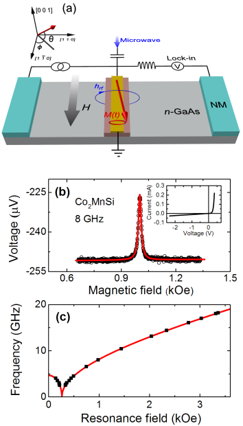
Figure 1(a) depicts the measurement geometry for our experiment, where is the in-plane angle relative to the crystal axis , which is the in-plane magnetic hard axis, and is the out-of-plane angle, measured relative to the (001) plane. For FMR measurements, the magnetic field is applied in the (001) plane. A dc bias current is combined with the microwave excitation signal using a bias-T and coupled into the sample using a coaxial cable. The microwave current passes through a 100 nm thick gold layer deposited on top of the FM contact, generating an in-plane Oersted field along the direction. We use a lock-in amplifier to measure the voltage of FM contact with respect to a CuGe (non-magnetic) counter electrode.Aboelfotoh et al. (1994) As the magnetic field is swept through the resonance, a dc voltage peak is measured. Figure 1(b) shows the resonance peak for a Co2MnSi sample. Similar peaks, all with a symmetric lineshape, are observed in the other two heterostructures. By varying the excitation frequency, the FMR frequency can be measured as a function of magnetic field, as shown using solid squares in Fig. 1(c). The frequency calculated from the Kittel formulaKittel (1948) is shown by the solid curve in Fig. 1(c). In applying the Kittel formula, the saturation magnetization and uniaxial anisotropy were determined from measurements of the saturation field along and directions.
Because the FMR measurement uses the 3-terminal configuration,Lou et al. (2006) the observed FMR peak corresponds to a change in the voltage across the FM/-GaAs interface. Careful characterization of the FM/-GaAs interface allows us to identify the mechanism responsible for this FMR peak. In these epitaxally grown samples, a Schottky tunnel barrier exists at the FM/-GaAs interface.Schmidt (2005) Spin-orbit interactions due to the Rashba field at the interface as well as the Dresselhaus field in the tunnel barrier lead to a dependence of the tunneling resistance on the orientation of the magnetization with respect to the crystal axes.Moser et al. (2007); Matos-Abiague et al. (2009) This phenomenon is called tunneling anisotropic magnetoresistance (TAMR) and is present in all of our samples.
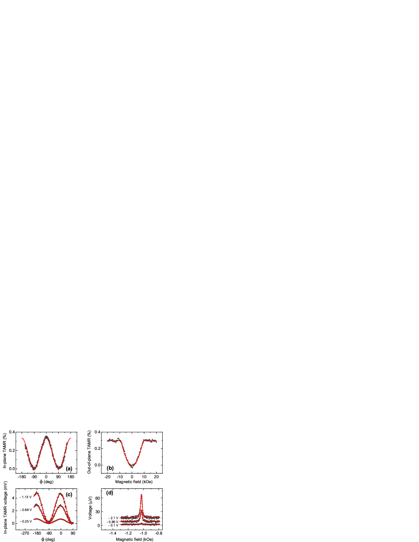
The TAMR effect is shown for a Co2MnSi device in Figs. 2(a) and (b). The in-plane TAMR , where is the interfacial resistance when the magnetization vector is oriented along , is shown as a function of in Fig. 2(a), and the out-of-plane TAMR is shown as a function of the out-of-plane field in Fig. 2(b). A linear background due to a slight misalignment of the sample has been subtracted. The observed TAMR effect in our heterostructures is similar in magnitude to the results from other studies of FM-GaAs interfaces.Uemura et al. (2011); Moser et al. (2007) The solid line in Fig. 2(a) is fit using a function, from which we obtain the magnitude of the in-plane TAMR. Given the ordinary shape anisotropy of a thin film, the out-of-plane TAMR should depend quadratically on magnetic field below saturation. A fit is shown using the solid curve in Fig. 2(b). The out-of-plane TAMR is the difference between the resistances measured at zero field, for which the magnetization lies along [110], and at saturation, for which it lies along [001]. The full angular dependence of the TAMR can be written as
| (1) |
where is the out-of-plane TAMR measured relative to the direction. Similar angular dependencies of the TAMR are observed for any bias voltage, as shown in Fig. 2(c) for the in-plane case. There is a marked similarity in the bias-dependence of the magnitude of the FMR peak, which is shown in Fig. 2(d).
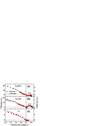
We now show that the FMR signals in Fig. 1 and Fig. 2(d) are due to TAMR. The primary evidence comes from a comparison of the bias voltage dependence of the magnitude of the FMR peak and the in-plane TAMR voltage . These are shown in Fig. 3 for all three FM materials. In each case, the FMR and TAMR signals under reverse bias () are directly proportional to each other. For clarity, the -scale for forward bias () is magnified by the factors shown for each sample. A similar scaling between the TAMR and FMR is observed for small forward bias voltages, although the proportionality breaks down as the forward bias voltage increases. This breakdown of scaling between FMR and TAMR is due to the existence of a spin accumulation, the consequences of which will be discussed in a future publication.
In a similar experiment carried out in a waveguide, in which the sample orientation can be changed with respect to the microwave field, we find that the peak shape is insensitive to the direction of the microwave electric field, in contrast to the case of rectification of ordinary AMR.Harder et al. (2011) This observation implies that the dc voltage generated by the FMR is sensitive only to the precessing magnetization and is independent of the microwave current flowing in the FM. The relevant mechanism is illustrated in Fig. 4(a), which shows the TAMR voltage as a function of and . When the FM contact is driven on resonance, the magnetization follows an elliptical trajectory in space. The resonant trajectory can be calculated from the known anisotropy surface, and the example for the case () is shown as the solid red curve in Fig. 4(a). On average, the TAMR voltage in the presence of a precessing magnetization increases relative to its equilibrium value at (). This effect is proportional to the local curvature of the TAMR surface and the square of the angular amplitude of precession.
To explore this effect more quantitatively, we investigate the dependence of the FMR peak on the in-plane orientation of the magnetization at a fixed reverse bias. This measurement is carried out in a waveguide, and the orientation of the microwave magnetic field is the same as in Fig. 1(a). Figure 4(b) shows the FMR peak magnitude observed from a Co2MnSi sample as a function of . The FMR peak is largest at and undergoes a sign change before approaching zero as .
From the above discussion, we can derive an expression for the magnitude of the FMR voltage peak as a function of the in-plane angle of the magnetization. We expand the interface voltage to second order in small deviations and about their equilibrium values. We retain only those terms that will not vanish after taking a time average:
| (2) | |||||
where is the interface bias current, and are the in-plane and out-of-plane precession cone angles respectively, and is the resonance frequency. With the substitution of the measured from Eq. 1 into Eq. 2 and taking of the time average, we obtain:
| (3) |
In Eq. 3, the sum of the last two terms, which depend on the precessional cone angles, is the voltage of the FMR peak. The precessional cone angles are and , where and are the in-plane and out-of-plane angular amplitudes at . The factor accounts for the change in the component of the microwave magnetic field perpendicular to the magnetization. Finally we obtain:
| (4) |
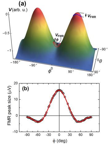
To calculate from Eq. 4, and are obtained from the TAMR measurement. Because of the shape anisotropy of the thin film, the second term involving the out-of-plane cone angle in Eq. 4 is significantly smaller than the first term. The magnitude of the FMR peak should therefore be proportional to , as observed in Fig. 3. The quadratic dependence on and implies that the FMR peak should be symmetric, in agreement with experiment. In Fig. 4(b) the solid curve is a fit of the in-plane angle dependence of the FMR signal using Eq. 4. The angular amplitudes and are the only fitting parameters. We find and for the in-plane and out-of-plane cone angles respectively. We calculated the dynamical susceptibility for this sample using the measured saturation magnetization and anisotropy, from which we find the ratio , in reasonable agreement with the value of 2.3 obtained from the fit of the angle dependence data in Fig. 4.
We emphasize that the mechanism discussed in this paper is essentially a modulation of the tunneling current due to the precession of the magnetization. This is distinct from spin pumping, in which a spin current is generated directly by the precessing magnetization. Because of the significant Schottky tunnel barrier present in these devices, we expect spin pumping effects to be small. In fact, we have not been able to observe any inverse spin Hall effect on resonance at zero bias, in spite of the fact that devices fabricated from the same heterostructures do function as non-local spin valves. On the other hand, the tunnel barrier in these samples enhances the TAMR effect. As noted above, we do observe a significant deviation of the FMR signal from the TAMR under forward bias voltages, as can be seen in Figs. 3(a) and (b). In determining the extent to which these deviations are due to spin accumulation, a reliable means for separating the TAMR component, as described here, is essential.
In summary, we have performed electrically detected FMR experiments on epitaxial FM/-GaAs heterostructures. We observe a strong dc voltage peak at the FM/-GaAs interface at resonance in a variety of heterostructures with different ferromagnets. In each case, the predominant origin of the FMR peak is the tunneling anisotropic magnetoresistance. This contribution must be considered in any measurement in which the FM/semiconductor interface is biased.
This work was supported by NSF under DMR-1104951, the MRSEC program of NSF under DMR 08-19885, and C-SPIN, one of the six centers of STARnet, a SRC program sponsored by MARCO and DARPA.
References
- Žutić et al. (2004) I. Žutić, J. Fabian, and S. Das Sarma, Rev. Mod. Phys. 76, 323 (2004).
- Tserkovnyak et al. (2002) Y. Tserkovnyak, A. Brataas, and G. E. W. Bauer, Phys. Rev. Lett. 88, 117601 (2002).
- Saitoh et al. (2006) E. Saitoh, M. Ueda, H. Miyajima, and G. Tatara, Appl. Phys. Lett. 88, 182509 (2006).
- Ando et al. (2011) K. Ando, S. Takahashi, J. Ieda, H. Kurebayashi, T. Trypiniotis, C. H. W. Barnes, S. Maekawa, and E. Saitoh, Nat. Mater. 10, 655 (2011).
- Kurebayashi et al. (2011) H. Kurebayashi, O. Dzyapko, V. E. Demidov, D. Fang, A. J. Ferguson, and S. O. Demokritov, Nat. Mater. 10, 660 (2011).
- Mecking et al. (2007) N. Mecking, Y. S. Gui, and C.-M. Hu, Phys. Rev. B 76, 224430 (2007).
- Chen et al. (2013) L. Chen, F. Matsukura, and H. Ohno, Nat. Commun. 4, (2013).
- Chen et al. (2014) L. Chen, S. Ikeda, F. Matsukura, and H. Ohno, Appl. Phys. Express 7, 013002 (2014).
- Lou et al. (2007) X. Lou, C. Adelmann, S. A. Crooker, E. S. Garlid, J. Zhang, K. S. M. Reddy, S. D. Flexner, C. J. Palmstrøm, and P. A. Crowell, Nat. Phys. 3, 197 (2007).
- Galanakis et al. (2002) I. Galanakis, P. H. Dederichs, and N. Papanikolaou, Phys. Rev. B 66, 134428 (2002).
- Wang et al. (2005) W. H. Wang, M. Przybylski, W. Kuch, L. I. Chelaru, J. Wang, Y. F. Lu, J. Barthel, H. L. Meyerheim, and J. Kirschner, Phys. Rev. B 71, 144416 (2005).
- Gercsi et al. (2006) Z. Gercsi, A. Rajanikanth, Y. K. Takahashi, K. Hono, M. Kikuchi, N. Tezuka, and K. Inomata, Appl. Phys. Lett. 89, 082512 (2006).
- Farshchi and Ramsteiner (2013) R. Farshchi and M. Ramsteiner, J. Appl. Phys. 113, 191101 (2013).
- Aboelfotoh et al. (1994) M. O. Aboelfotoh, C. L. Lin, and J. M. Woodall, Appl. Phys. Lett. 65, 3245 (1994).
- Kittel (1948) C. Kittel, Phys. Rev. 73, 155 (1948).
- Lou et al. (2006) X. Lou, C. Adelmann, M. Furis, S. A. Crooker, C. J. Palmstrøm, and P. A. Crowell, Phys. Rev. Lett. 96, 176603 (2006).
- Schmidt (2005) G. Schmidt, J. Phys. D: Appl. Phys. 38, R107 (2005).
- Moser et al. (2007) J. Moser, A. Matos-Abiague, D. Schuh, W. Wegscheider, J. Fabian, and D. Weiss, Phys. Rev. Lett. 99, 056601 (2007).
- Matos-Abiague et al. (2009) A. Matos-Abiague, M. Gmitra, and J. Fabian, Phys. Rev. B 80, 045312 (2009).
- Uemura et al. (2011) T. Uemura, M. Harada, T. Akiho, K.-i. Matsuda, and M. Yamamoto, Appl. Phys. Lett. 98, 102503 (2011).
- Harder et al. (2011) M. Harder, Z. X. Cao, Y. S. Gui, X. L. Fan, and C.-M. Hu, Phys. Rev. B 84, 054423 (2011).