†Present address: Department of Chemical Engineering, Stanford University, Stanford, California 94305, USA.
⋆22email: eltonjos@stanford.edu
Electric Field Effects on Graphene Materials
Abstract
Understanding the effect of electric fields on the physical and chemical properties of two-dimensional (2D) nanostructures is instrumental in the design of novel electronic and optoelectronic devices. Several of those properties are characterized in terms of the dielectric constant which play an important role on capacitance, conductivity, screening, dielectric losses and refractive index. Here we review our recent theoretical studies using density functional calculations including van der Waals interactions on two types of layered materials of similar two-dimensional molecular geometry but remarkably different electronic structures, that is, graphene and molybdenum disulphide (MoS2). We focus on such two-dimensional crystals because of they complementary physical and chemical properties, and the appealing interest to incorporate them in the next generation of electronic and optoelectronic devices. We predict that the effective dielectric constant () of few-layer graphene and MoS2 is tunable by external electric fields (). We show that at low fields ( V/Å) assumes a nearly constant value 4 for both materials, but increases at higher fields to values that depend on the layer thickness. The thicker the structure the stronger is the modulation of with the electric field. Increasing of the external field perpendicular to the layer surface above a critical value can drive the systems to an unstable state where the layers are weakly coupled and can be easily separated. The observed dependence of on the external field is due to charge polarization driven by the bias, which show several similar characteristics despite of the layer considered. All these results provide key information about control and understanding of the screening properties in two-dimensional crystals beyond graphene and MoS2.
1 Introduction
Electron-electron interactions play a central role on a wide range of electronic phenomena in two-dimensional (2D) materials. One of the main ingredients that determines the Coulomb interaction strength in those systems is screening, which can be characterized by dielectric constant, . Indeed, screening effects based on play a fundamental role in determining the electron dynamics, the optical exciton binding energy, the electron and hole mobilities as well as charge storage features. In this context the Coulomb interactions are confined in a two-dimensional geometry which can give place to a new set of dielectric properties depending on the electronic nature of the 2D crystal.
Graphene, a semimetal with zero bandgap, and MoS2, a low-dimension direct band gap semiconductor, are two representative members of the 2D family that have been receiving much attention in many fields due to their remarkable chemical and physical properties (Castro Neto et al. 2009, Wang et al. 2012). One of the main features that influences all these properties is the layer thickness, which determines the charge distribution in the device as well as the electronic structure through the band gap. In particular, graphene can become a semiconductor with a band gap of several tenths of meV’s at a bilayer structure subjected to high electric gate bias (Castro et al. 2007). MoS2, in its turn, has a sizable band gap that varies as a function of the number of layers which reaches values of about 1.8 eV at the monolayer limit (Mak et al. 2010). In both situations the electric-field screening is observed to change as the dielectric response depends on the intrinsic electronic properties as well as on .
In fact, the large range of values for found by different experiments on graphene (Elias et al. 2011, Siegel et al. 2011, Bostwick et al. 2010, Reed at al. 2010, Wang et al. 2012, Sanchez-Yamagishi et al. 2012, Fallahazad et al. 2012, Jellison et al. 2007) and MoS2 (Zhang et al. 2012, Kim et al. 2012, Bell et al. 1976, Frindt et al. 1963, Beal et al. 1979) has become a subject of considerable discussions. More factors, apart from the external electric fields and layer thickness, indicate that might depend on the underneath substrate as recently measured for graphene (Hwang et al. 2012) and MoS2 layers (Bao et al. 2013). In practical terms, the dielectric constant is defined by /2, with and the dielectric constant values for the substrate and vacuum, respectively. However, this approach suggests that the environment could play a role in the determination of the intrinsic dielectric constant of these 2D materials. Therefore, it is paramount to determine the intrinsic value of despite of external screening environments.
In the present Chapter, we provide a review of some of our recent computational studies on the effect of electric fields on multilayer graphene and MoS2. We will consider both layered systems at different field magnitudes (0-1.0 V/Å) and number of layers (2L-10L). Some differences on the dielectric response between graphene and MoS2 will be discussed based on simple electrostatic concepts, which will give generality to the calculations for other 2D-layers still to be explored.
2 Electrical Field Tuning of the Dielectric Constant

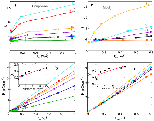
Figure 1a, c display how evolves with external fields for different number of graphene and MoS2 layers, respectively. At low fields, 0.001 V/Å, is almost independent of the number of layers having a value close to for both two-dimensional crystals. As the external field is increased, reaches larger values, up to 12.0 at E1.0 V/Å for graphene layers. Similar electric response is observed for MoS2 with 16.8 at 0.8 V/Å for layers with an approximately linear dependence of on the number of layers at a fixed magnitude of the field. These values for are in good agreement with those found by experimental groups working on graphene (Elias et al. 2011, Siegel et al. 2011, Bostwick et al. 2010, Reed at al. 2010, Wang et al. 2012, Sanchez-Yamagishi et al. 2012, Fallahazad et al. 2012, Jellison et al. 2007) and on MoS2(Zhang et al. 2012, Kim et al. 2012, Bell et al. 1976, Frindt et al. 1963, Beal et al. 1979) samples. The electric susceptibility extracted from the polarization clearly shows the roughly linear dependence on the number of layers as plotted in Fig. 1b, d. Moreover, the comparison between graphene and MoS2 also gives that the tuning of with the external field is larger to the latter. At , is 0.95 for multilayer MoS2 and 0.42 for multilayer graphene, which is less than half of that value calculated for MoS. This suggests that the dichalcogenide layer is more electrically polarizable than graphene.
We note that electric fields of the magnitude considered here can in principle be experimentally created, as recently obtained in the case of 3L graphene (Zou et al. 2013) which fields close to 0.6 V/Åwere achieved taking into account HfO2 gates. In the case of MoS2, the high dielectric breakdown, due to the chemical character of the MoS covalent bonds, allows the application of large electric bias as recently reported in voltage-current measurements (Lembke et al. 2012).
3 Interlayer Electric Field: Spatial Dependence

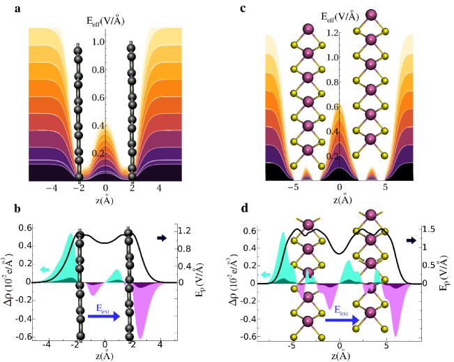
Next we discuss the origin of the electric-field mediated tunable dielectric constant in graphene and MoS2 layered systems. Figure 2 shows the electric response in terms of the effective electric field calculated from the Hartree potential along the supercell for bilayer structures. The application of the external field generates an interlayer charge-transfer which partially cancels inducing the appearance of in the region between the layers. At low , all the induced values of are approximately constant, within the numerical accuracy of our model, assuming similar shapes as displayed in the dark regions of Fig. 2a,c. At fields close to those used to modify the band gap of 2L graphene (Mak et al. 2009, Zhang et al. 2009, Castro et al. 2007), or used in MoS2 transistors (Radisavljevic et al. 2011), that is 0.08 V/Å, the effective field Eeff is already dependent on position z, with a maximum at the mid-point between the layers. MoS2 has the difference to be formed by SMoS bonds perpendicular to the external field, which induce a smaller but finite contribution between the S atoms. Moreover, the effective field on 2L MoS2 assumes a narrower a shape relative to graphene with negligible values close to S. The electric response can also be analyzed based on the the induced charge densities, , at different fields as plotted in Figure 2b,d. Both layered systems show a charge accumulation at the layer that is under positive potential and a corresponding depletion at the other one . The integration of along z, utilizing the Poisson equation , where is the vacuum permittivity, results in a response electric field (solid black line in Figure 2b,d) that screens the external electric field, that is, - .
4 Electric Field Damping in Multilayer Systems

In the previous section, we have considered in detail the the electric response due to external fields on graphene and MoS2 2L structures. Although this is an important system, other aspects are also crucial to understand and control the screening associated to two-dimensional crystals. For example, one needs to explore the characteristics of multilayer systems subjected to external bias, as well as the possibility to compare structures with different electronic character. This kind of knowledge is instrumental in possible applications in electronics and optoelectronics.
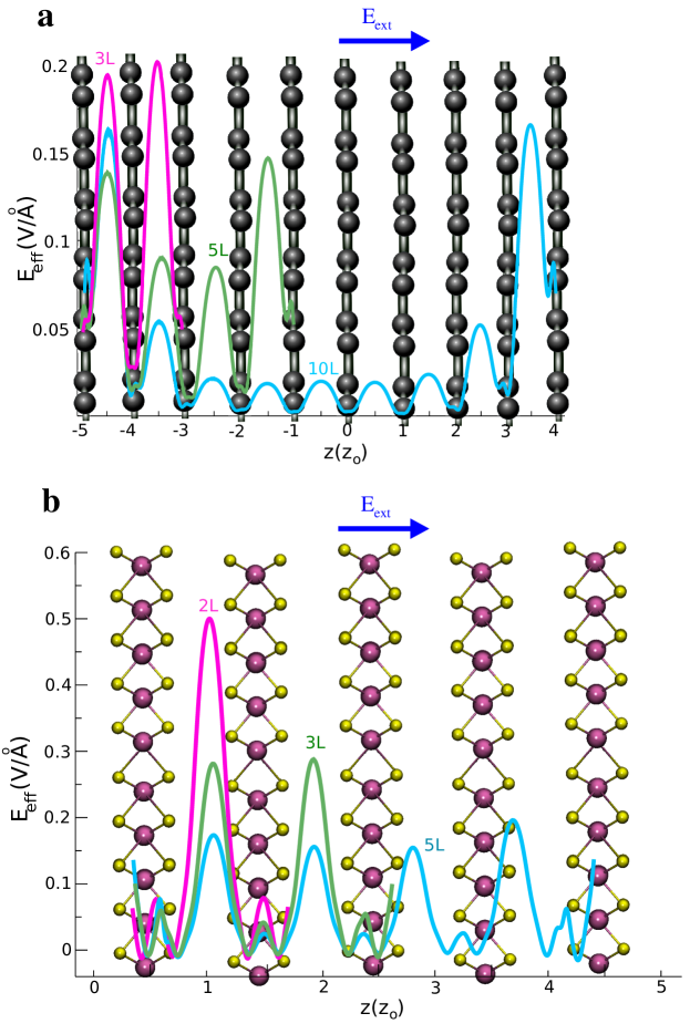
We address next the dependence of as a function of the number of graphene and MoS2 layers as shown in Figure 3. Despite the electronic character of each system, the application of Eext on thicker structures creates higher Eeff in the first few layers with a reduction of field in the innermost regions of the structure. For example in graphene, in the case, the maximum value of Eeff between the two carbon layers at and is 3.2 times larger than that between the layers at and . In deeper layers, the field decays further reaching even smaller values. For MoS2, the outermost layers show a slightly higher Eeff and the field decay follows that observed for graphene. However, the damping between internal and external layers, that is, those closer to the gate bias, is slightly different as that observed at the carbon planes. This suggests that the charge polarization of the layers due to the different electronic character (Fig. 1c,d) plays an important role on the screening behavior and also on the electrical tuning of the dielectric constant with the number of layers. As is calculated by the ratio of the external and internal fields to the slabs, the enhancement in the value of the dielectric constant with the number of layers is directly related to the reduction of the field in the innermost regions of the structure which leads to lower values for lower values of . This decay of field with the layer thickness is in good agreement with recent electrostatic force microscopy and Kelvin probe microscope measurements performed for MoS2 (Castellanos-Gomez et al. 2013, Li et al. 2013) and graphene (Datta et al. 2009).
5 Electrostatic Exfoliation on Graphene and MoS2 Layers

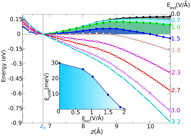
In this section we analyze the possibility to use an electrostatic gate that can be used to exfoliate graphene and MoS2 layers at different bias. We note that there is an upper limit on the magnitude of that can be applied to the systems as the bias induces a shift of the equilibrium position of the layers to higher interlayer separations. Figure 4 displays the total energy for MoS2 2L as a function of the interlayer distance . We focus on MoS2 since similar effects are observed for graphene. At 0.0 V/Å, a van der Waals barrier of 30 meV/atom prevents the separation of the two layers from zo to infinity. At finite , the value of decreases, indicating that the MoS2-layers become less bound. At 2.0 V/Å, the two dichalcogenide layers can be easily separated with a barrier of only 0.45 meV/atom. This indicates that an electrostatic gate can be utilized for exfoliating and printing few-layers MoS2 in pre-pattern form similarly to that observed for graphene (Lian et al. 2009). Since several challenges of making industrially available large-scale areas of 2D-crystals and fabricating atomic features with precise electronic structure are still to be overcome, the electrostatic exfoliation shown in our calculations could open new avenues for the achievement of such desired properties.
6 Conclusions
In this Chapter we have reviewed the electrical response of two representative layered materials for future devices-based on graphene and MoS2. We have focused on the interplay between electric fields and screening properties of few-layer structures. Density functional theory was the main tool used to compute the properties of the analyzed systems. We have used simple models to understand the observed trends. In particular, we find that the effective dielectric constant of graphene and MoS2 is electrically tunable, with the layer thickness playing an important role in the enhancement of the effect. The thicker the structure is, the stronger the modulation with electric fields. The driving force for such behavior is due to the linear dependence of the electrical polarization of the layers on the external field. The response field computed from the polarization charge does not screen completely the external bias, which generate higher interlayer fields at thinner structures. Differences due to semi-metallic and semiconducting electronic character of the layers are observed in terms of the field damping inside of the compounds: graphene tends to screen the external field at the outermost layers of system, while MoS2 the field penetrates deeper in the layers. These results are in sound agreement with recent experiments performed for both materials.
We have also explored the possibility to control the layer exfoliation using electric fields. We have found that the induced interlayer charge imbalance generated by the bias can drive the system to an unstable state where the layers can be separated from each other. The interlayer equilibrium position is modified as a function of the field magnitude, which induces a reduction of the van der Waals barrier that keeps the layers together. As a result, there are variations of the interlayer separations even at low-fields. This investigation is highly relevant in the interpretation of experimental results underway since the field of 2D-materials is just in its beginning where several techniques and effects are still to be developed and explored.
References
- (1) Castro Neto, A. H., Guinea, F., Peres, N. M. R., Novoselov, K. S., Geim, A. K. The electronic properties of graphene. Rev. Mod. Phys. 2009, 81, 109-162.
- (2) Wang, Q. H.; Kalantar-Zadeh, K.; Kis, A.; Coleman, J. N.; Strano, M. S. Electronics and Optoelectronics of Two-dimensional Transition Metal Dichalcogenides. Nat. Nanotechnol. 2012, 7, 699-712.
- (3) Castro, E. V., Novoselov, K. S., Morozov, S. V., Peres, N. M. R., dos Santos, J. M. B. Lopes, Nilsson, J., Guinea, F., Geim, A. K., Castro-Neto, A. H. Biased Bilayer Graphene: Semiconductor with a Gap Tunable by the Electric Field Effect. Phys. Rev. Lett. 2007, 99, 216802-216806.
- (4) Mak, K. F.; Lee, C.; Hone, J.; Shan, J.; Heinz, T. F. Atomically Thin MoS2: a New Direct-Gap Semiconductor. Phys. Rev. Lett. 2010, 105, 136805-136809.
- (5) Elias, D. C., Gorbachev, R. V., Mayorov, A. S., Morozov, S. V., Zhukov, A. A., Blake, P., Ponomarenko, L. A., Grigorieva, I. V., Novoselov, K. S., Guinea, F., Geim, A. K. Dirac cones reshaped by interaction effects in suspended graphene. Nature Phys. 2011, 7, 701-704.
- (6) Siegel, D. A., Park, C. H., Hwang, C. Deslippe, J., Fedorov, A. V., Louie, S. G., Lanzara, A. Many-body interactions in quasi-freestanding graphene. Proceedings of the National Academy of Sciences 2011, 108, 11365-11370.
- (7) Bostwick, A., Speck, F., Seyller, T., Horn, K., Polini, M., Asgari, R., MacDonald, Allan H., Rotenberg, E. Observation of Plasmarons in Quasi-Freestanding Doped Graphene. Science 2010, 328, 999-1002.
- (8) Reed, J. P., Uchoa, B., Joe, Y. I., Gan, Y., Casa, D., Fradkin, E., Abbamonte, P. The Effective Fine-Structure Constant of Freestanding Graphene Measured in Graphite. Science 2010, 330, 805-808.
- (9) Wang, Y., Brar, V. W., Shytov, A. V., Wu, Q., Regan, W., Tsai, H. Z., Zettl, A., Levitov, L. S., Crommie, M. F. Mapping Dirac Quasiparticles near a Single Coulomb Impurity on Graphene. Nature Phys. 2012, 8, 653-657.
- (10) Sanchez-Yamagishi, J. D., Taychatanapat, T., Watanabe, K., Taniguchi, T., Yacoby, A., Jarillo-Herrero, P. Quantum Hall Effect, Screening, and Layer-Polarized Insulating States in Twisted Bilayer Graphene. Phys. Rev. Lett. 2012, 108, 076601-076606.
- (11) Fallahazad, B., Hao, Y., Lee, K., Kim, S., Ruoff, R. S., Tutuc, E. Quantum Hall effect in Bernal stacked and twisted bilayer graphene grown on Cu by chemical vapor deposition. Phys. Rev. B 2012, 85, 201408-201413.
- (12) Jellison, G. E., Hunn, J. D., Lee, Ho N. Measurement of optical functions of highly oriented pyrolytic graphite in the visible. Phys. Rev. B 2007, 76, 085125-085133.
- (13) Zhang, X.; Hayward, D. O.; Mingos, D. M. P. Dielectric Properties of MoS2 and Pt Catalysts: Effects of Temperature and Microwave Frequency. Catal. Lett. 2002, 84, 225-233.
- (14) Kim, S.; Konar, A.; Hwang, W. S.; Lee, J. H.; Lee, J.; Yang, J.; Jung, C.; Kim, H.; Yoo, J. B.; Choi, J. Y.; et al. High-Mobility and Low-Power Thin-Film Transistors Based on Multilayer MoS2 Crystals. Nat. Commun. 2012, 3, 1011-1018.
- (15) Bell, M. G.; Liang, W. Y. Electron Energy Loss Studies in Solids: The Transition Metal Dichalcogenides. Adv. Phys. 1976, 1976, 53-86.
- (16) Frindt, R. F.; Yoffe, A. D. Physical Properties of Layer Structures: Optical Properties and Photoconductivity of Thin Crystals of Molybdenum Disulphide. Proc. Roy. Soc. A 1963, 273, 69-83.
- (17) Beal, A. R.; Hughes, H. P. Kramers-Kronig Analysis of the Reflectivity Spectra of 2H-MoS2, 2H-MoSe2 and 2H-MoTe2. J. Phys. C: Solid State Phys. 1979, 12, 881-890.
- (18) Hwang, C., - Siegel, David A., Mo, S. K., Regan, W., Ismach, A., Zhang, Y., Zettl, A., Lanzara, A. Fermi velocity engineering in graphene by substrate modification. Sci. Rep. 2012, 2:590.
- (19) Bao, W.; Cai, X.; Kim, D.; Sridhara, K.; Fuhrer, M. S. High Mobility Ambipolar MoS2 Field-Effect Transistors: Substrate and Dielectric Effects. Appl. Phys. Lett. 2013, 102, 042104-042108.
- (20) Santos, E. J. G.; Kaxiras, E. Electric-Field Dependence of the Effective Dielectric Constant in Graphene. Nano Lett. 2013, 13, 898-902.
- (21) Santos, E. J. G.; Kaxiras, E. Electrically-Driven Tuning of the Dielectric Constant in MoS2 Layers. ACS Nano 2013, 7, 10741–10746.
- (22) Zou, K.; Zhang, Fan; Clapp, C.; MacDonald, A. H.; Zhu, J. Transport Studies of Dual-Gated ABC and ABA Trilayer Graphene: Band Gap Opening and Band Structure Tuning in Very Large Perpendicular Electric Fields. Nano Lett. 2013, 13, 369-373.
- (23) Lembke, D.; Kis, A. Breakdown of High-Performance Monolayer MoS2 Transistors. Nano Lett. 2012, 6 10070-10075.
- (24) Radisavljevic, B.; Radenovic, A.; Brivio, J.; Giacometti, V.; Kis, A. Single-Layer MoS2 Transistors. Nat. Nanotechnol. 2011, 6, 147-150.
- (25) Mak, K. F., Lui, C. H., Shan, J., Heinz, T. F. Observation of an Electric-Field-Induced Band Gap in Bilayer Graphene by Infrared Spectroscopy. Phys. Rev. Lett. 2009, 102, 256405-256409.
- (26) Zhang, Y., Tang, T. T., Girit, C., Hao, Z., Martin, M. C., Zettl, A., Crommie, M. F., Shen, Y. R., Wang, F. Direct observation of a widely tunable bandgap in bilayer graphene. Nature 2009, 459, 820-823.
- (27) Castellanos-Gomez, A.; Cappelluti, E.; Roldán, R.; Agrait; N., Guinea; F.; Rubio-Bollinger, G. Electric-Field Screening in Atomically Thin Layers of MoS2: the Role of Interlayer Coupling. Adv. Mater. 2013, 25, 899-903.
- (28) Li, Y.; Xu, C.-Y.; Zhen, L. Surface Potential and Interlayer Screening Effects of Few-Layer MoS2 Nanoflakes. Appl. Phys. Lett. 2013, 102, 143110-143114.
- (29) Datta, S. S.; Strachan, D. R.; Mele, E. J.; Johnson, A. T. C. Surface Potentials and Layer Charge Distributions in Few-Layer Graphene Films. Nano Lett. 2009, 9, 7-11.
- (30) Liang, X., Chang, A. S. P., Zhang, Y., Harteneck, B. D., Choo, H., Olynick, D. L., Cabrini, S. Electrostatic Force Assisted Exfoliation of Prepatterned Few-Layer Graphenes into Device Sites. Nano Letters 2009, 9 467-472.