High Intrinsic Mobility and Ultrafast Carrier Dynamics in Multilayer Metal Dichalcogenide MoS2
Abstract
The ultimate limitations on carrier mobilities in metal dichalcogenides, and the dynamics associated with carrier relaxation, are unclear. We present measurements of the frequency-dependent conductivity of multilayer dichalcogenide MoS2 by optical-pump terahertz-probe spectroscopy. We find mobilities in this material approaching 4200 cm2V-1s-1 at low temperatures. The temperature dependence of scattering indicates that the mobility, an order of magnitude larger than previously reported for MoS2, is intrinsically limited by acoustic phonon scattering at THz frequencies. Our measurements of carrier relaxation reveal picosecond cooling times followed by recombination lasting tens of nanoseconds and dominated by Auger scattering into defects. Our results provide a useful context in which to understand and evaluate the performance of MoS2-based electronic and optoelectronic devices.
Layered two-dimensional transition metal dichalcogenides have recently enjoyed a resurgence of interest from the scientific community both from a new science perspective and also for novel applicationsPodzorov et al. (2004); Splendiani et al. (2010); Mak et al. (2010); Eda et al. (2011); Yoon et al. (2011); Cao et al. (2012); Kioseoglou et al. (2012); van der Zande et al. (2013); Zhou et al. (2013); Wang et al. (2012a). In contrast to graphene, metal dichalcogenides have non-zero bandgaps and are also efficient light emitters, making them attractive for electronics and optoelectronicsPodzorov et al. (2004); Splendiani et al. (2010); Mak et al. (2010); Eda et al. (2011); Yoon et al. (2011); Cao et al. (2012); Kioseoglou et al. (2012); van der Zande et al. (2013); Zhou et al. (2013); Wang et al. (2012a). The ability to synthesize atomically thin semiconducting crystals and their heterostructures and transfer them to arbitrary substrates has opened the possibility of transparent, flexible electronics and optoelectronics based on these material systemsWang et al. (2012a, b); Laskar et al. (2013); Lopez-Sanchez et al. (2013); Perkins et al. (2013); Malard et al. (2013); Zhu et al. (2014); Mak (2014). The best reported carrier mobilities in metal dichalcogenides, typically in the few hundred cm2V-1s-1 range for MoS2Das et al. (2013); Bao et al. (2013), are not as large as in graphene. But the reported mobilities are large in comparison to those of organic materials often used for flexible electronicsPodzorov et al. (2004). Physical mechanisms limiting the mobility of monolayer and multilayer MoS2 field effect transistors have been the subject of several experimentalFivaz and Mooser (1967); Das et al. (2013); Kim et al. (2012); Bao et al. (2013); Pradhan et al. (2013); Radisavljevic and Kis (2013); Kumar et al. (2013) and theoreticalKaasbjerg et al. (2012); Ma and Jena (2014) investigations. Charged impurity scattering, electron-phonon interaction, and screening by the surrounding dielectric environment are all believed to affect the mobility. Due to the challenge of isolating these effects, the intrinsic mobility of MoS2, and the ultimate performance of electronic devices, remains unclear. Similarly, carrier intraband and interband scattering and relaxation rates, which determine the performance of almost all proposed and demonstrated electronic and optoelectronic metal dichalcogenide devices, remain poorly understood.
In this report, we present optical-pump THz-probe measurements of the time- and frequency-dependent conductivity of multilayer MoS2. Previously reported electrical measurementsDas et al. (2013); Kim et al. (2012); Bao et al. (2013); Pradhan et al. (2013) have probed the MoS2 DC carrier transport, and all-optical measurementsKorn et al. (2011); Kumar et al. (2013) have probed the exciton temporal dynamics. In contrast, optical-pump THz-probe spectroscopy can measure the time development of the complex intraband conductivity in the 0.2-2.0 THz frequency range with a temporal resolution better than a few hundred femtoseconds. The frequency dependence of the measured intraband conductivity leads to the direct extraction of the carrier momentum scattering rate, from which the carrier mobility can be determined in a contact-free way. In addition, the temporal development of the intraband conductivity reveals carrier interband and intraband relaxation dynamics.
Our results show that the momentum scattering times in multilayer MoS2 vary from 90 fs at 300 K to 1.46 ps at 30 K, corresponding to carrier mobilities of 257 and 4200 cm2V-1s-1, respectively. The temperature dependence of the momentum scattering rate reveals that the mobility is limited by acoustic phonon scattering and the measured scattering times agree well with the theoretical predictionsKaasbjerg et al. (2012); Ma and Jena (2014). The measured mobility values are almost an order of magnitude larger than the previously reported values in multilayer MoS2 devicesFivaz and Mooser (1967); Kim et al. (2012); Bao et al. (2013). Our results indicate that the mobilities in reported MoS2 electronic devicesFivaz and Mooser (1967); Das et al. (2013); Kim et al. (2012); Pradhan et al. (2013); Radisavljevic and Kis (2013) are likely limited by extrinsic mechanisms (defects, impurities, grain boundaries, etc.) and point to the ultimate performance of metal dichalcogenide electronic devices. Our measurements of carrier relaxation reveal picosecond cooling times varying from 0.7 ps at 300 K to 1.2 ps at 45 K. Subsequent density-dependent recombination of carriers occurs over 10’s of nanoseconds at low temperature. We present a recombination model based on carrier capture into defect states which reproduces the measured nonlinearity of this recombination versus carrier density as well as the observed temporal dynamics.
I Results
I.1 Conductivity spectra and momentum scattering times
THz-frequency radiation is sensitive to the frequency-dependent intraband conductivity of MoS2, , which contains information about carrier scattering and mobility. Using a THz time-domain spectrometerKatzenellenbogen and Grischkowsky (1991), we measure the amplitude and phase of broadband THz pulses transmitted through our 4 m thick natural MoS2 samples. In a static transmission measurement, where the conductivity is time-independent, the thin-film () amplitude transmission for THz pulses is (see supplementary information),
| (1) |
where is the frequency, is the sample thickness, is the speed of light, is the impedance of free space, is the sample refractive index. Using Equation 1 and the measured spectra of THz pulses transmitted through an unpumped multilayer MoS2 sample, we obtained a constant value of refractive index in the 0.2-2.0 THz frequency range. Further, the unpumped DC conductivity was found to be in the range 10-20 S m-1 indicating that the sample was very mildly doped. Electrical measurements on similar single-layer and multilayer samples have indicated that these MoS2 samples tend to be n-dopedZhang et al. (2014). Given the large value of the refractive index and the small value of , this unpumped transmission measurement could not reliably determine the frequency dependence of the conductivity and thereby the mobility. In contrast, since the change in THz transmission, , between pumped and unpumped samples is directly proportional to the change in the conductivity , optical-pump THz-probe spectroscopy is a highly-sensitive method to extract the frequency-dependent conductivity.
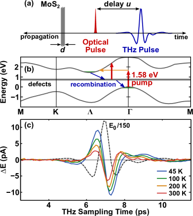
In the optical-pump THz-probe scheme, depicted in Figure 1(a-b), 780 nm center wavelength (1.58 eV), sub-100 fs optical pulses excite electron and hole distributions at the six points and the point, respectively, after which the distributions cool and recombine. The field of the THz pulse transmitted through the pumped sample, , is sensitive to the evolving conductivity and, therefore, depends on the pump-probe delay . In our experiments, the incident optical and THz pulses are mechanically chopped at different frequencies and the transmitted THz pulse is measured at the sum frequency. We therefore measure the change in the transmitted THz pulse, , in the presence () and absence () of optical pumping. In this paper, the symbol signifies the change in a quantity due to optical pumping. Figure 1(c) shows the measured for a fixed delay of ps at different temperatures. We also display , which was essentially temperature-independent. contains information of both the amplitude and phase changes of upon pumping. Comparison of and shows a trend of increasing phase shifts with decreasing temperatures due to photoexcited carriers. Thus, both the amplitude and the phase of the transmitted THz pulse are needed to determine the sample response.
The sample response can be determined from the measured change in the transmitted THz pulse, , as follows. We scan the pump-probe delay simultaneously with the transmitted THz pulse in the time-domain THz spectrometer such that each measured point of the transmitted THz pulse is at the same delay, , from the pumpKindt and Schmuttenmaer (1999); Beard et al. (2000); Nienhuys and Sundström (2005). The measured pulse, , satisfies (see supplementary information),
| (2) |
where is the permittivity of free-space. Equation 2 describes the effect of the free-carrier and polarization current densities on the THz pulse. The change in the free-carrier current density, , in the sample can be written approximately as (see supplementary information),
| (3) |
Here, is the change in the DC conductivity and is the normalized current impulse response (). In Fourier domain, we define as . Techniques to extract from the measured are described in the Methods section.
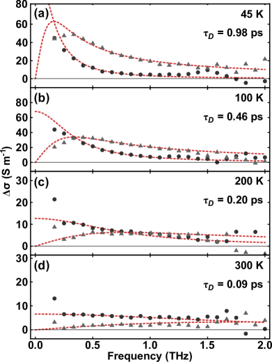
Figure 2 shows the real and imaginary parts of the photoexcited conductivity measured at four different temperatures in MoS2. We find that the measured conductivity spectra closely follow the Drude form, , which is the simplest conductivity model in the relaxation time approximation. Therefore, the current impulse response is . We fit the real and imaginary parts of the data simultaneously with a weighted least-squares regression and extract the photoexcited DC conductivity and the carrier momentum scattering time . Weights were the data variance at each frequency point over twenty scans. The high quality of fits to the data obtained at all temperatures, as shown in Figure 2, is strong evidence of the fact that the change in THz transmission we measure indeed originates from the intraband conductivity of the photoexcited carriers. Also, at all temperatures we find no significant variation in the extracted value of for any value of in the range 5 ps 12 ns. Since one expects very hot carriers to have average momentum scattering times different from that of cold carriersJnawali et al. (2013), this observation suggests that the carrier distributions after photoexcitation cool down on time scales shorter than a few picoseconds. We further discuss carrier cooling times below.
I.2 Carrier mobility
Carrier in-plane ( to c-axis) mobility is related to the momentum scattering time by , where is the in-plane conductivity effective mass. Multilayer MoS2 has six electron pockets in the Brillouin zone, each with an anisotropic effective mass tensorPeelaers and Van de Walle (2012); Zahid et al. (2013). The one hole pocket has an isotropic effective mass tensor. Using DFT values for the electron and hole effective mass tensorsPeelaers and Van de Walle (2012), we find the conductivity effective masses for both electrons and holes to be 0.61. In Figure 3(a), we plot the electron mobilities corresponding to the measured momentum scattering times at different temperatures ( = 30, 45, 100, 200, 300 K). We find a mobility of 257 cm2V-1s-1 at 300 K, increasing to 4200 cm2V-1s-1 at 30 K. For 300 K, the measured mobility is consistent with recent electronic transport measurements in multilayer MoS2Das et al. (2013); Kim et al. (2012); Bao et al. (2013); Pradhan et al. (2013); Fivaz and Mooser (1967). But the mobilities we find below 200 K in this contact-free measurement are significantly higher than the values previously reported for MoS2.
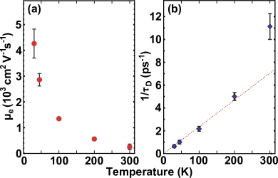
In Figure 3(b), we plot the carrier momentum scattering rate, , versus temperature. The scattering rate for K increases linearly with temperature. This linear temperature dependence is expected for quasi-elastic acoustic phonon scattering in 2D and layered materials in the equipartition regimeFivaz and Mooser (1967); Kawamura and Das Sarma (1992); Kaasbjerg et al. (2012); Ma and Jena (2014). Other scattering mechanisms, such as impurity scattering, have a different temperature dependence for layered materialsMa and Jena (2014). The larger scattering rate observed at the highest temperature (300 K) likely indicates an optical phonon scattering contributionKaasbjerg et al. (2012); Kim et al. (2012). In the deformation-potential approximation, the energy-independent acoustic-phonon-limited momentum scattering rate in 2D and layered materials is related to the temperature byKaasbjerg et al. (2012); Ma and Jena (2014),
| (4) |
where is the deformation potential, is the 2D mass density, is the LA phonon velocity, and is the carrier density of states effective mass. From the data in Figure 3(b), we find ns-1K-1 for K. Using m s-1Kaasbjerg et al. (2012), kg m-2, (ab-initio values for are almost identical for electrons and holesPeelaers and Van de Walle (2012)), we find eV. This value compares well with previously experimentally and theoretically determined values, generally in the 2-10 eV range, for the deformation potentials in single-layer and multilayer MoS2Cheiwchanchamnangij and Lambrecht (2012); Peelaers and Van de Walle (2012); Feng et al. (2012); He et al. (2013); Kaasbjerg et al. (2012).
I.3 Carrier dynamics on short time scales
Knowing and , we determine the photoexcited DC conductivity, (see Methods). The temporal resolution in our experiments is set by the measurement bandwidth of , 1.8 THz, and is approximately ps. Since the in-plane conductivity effective masses for electrons and holes are approximately the same in multilayer MoS2Peelaers and Van de Walle (2012), one can write the DC conductivity as , where is the total mobile carrier density and equals the sum of the mobile electron density, , and the mobile hole density, . The change in the carrier density can be determined from the measurement of .
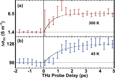
Figure 4 shows the measured change in the conductivity on short time scales ( ps) for two different representative temperatures. The pump fluence in each case is 1.2 J/cm2. Immediately after photoexcitation (), the conductivity increases, reaching its maximum value within 5 ps at all temperatures. The error-range displayed for each data point represents a 95% confidence interval for the fitting parameter . The dashed lines superimposed on the data represent fittings using exponential curves with 0.7 ps and 1.2 ps time constants at 300 K and 45 K, respectively. Our data suggests that the conductivity reaches its peak value faster at higher temperatures. As we discuss below, we attribute these short-time-scale dynamics to picosecond cooling of the electron and hole distributions.
As depicted in Figure 1(b), the 1.58 eV pump photons excite electrons from the valence band maximum at the point to the conduction band minima at the point by a phonon-assisted (or impurity-assisted) indirect absorption process. Since the indirect bandgap in multilayer MoS2 is around 1.29 eVMak et al. (2010); Cheiwchanchamnangij and Lambrecht (2012), the photoexcited electrons and holes are at an elevated temperature compared to the lattice immediately after photoexcitation and thermalizationJnawali et al. (2013); Wang et al. (2010). If the photon energy in excess of the indirect bandgap contributes to the kinetic energy of the carriers, we estimate the carrier temperature immediately after photoexcitation to be around 1100 K. At this high temperature, the electron and hole distributions would be spread out in energy, with fast momentum scattering rates and reduced mobility due to optical phononsKaasbjerg et al. (2012); Lundstorm (2009). As the carrier distributions relax towards the band extrema and cool via optical phonon emission, the carrier momentum scattering rates decrease and the conductivity increases. The rise in the conductivity following photoexcitation observed in our experiments is therefore indicative of carrier cooling. The slower cooling observed at lower lattice temperatures can be attributed to a number of factors. For example, the carrier cooling rates due to optical phonon emission are proportional to , where , the Bose occupation factor for phonons, is aproximately 20% larger at 300 K compared to 45 K. In addition, the heat capacity of optical phonons is around three orders of magnitude larger at 300 K compared to 45 K and, therefore, carrier cooling bottleneck due to the generation of hot phonons is much reduced at higher lattice temepraturesWang et al. (2010).
I.4 Carrier dynamics on long time scales
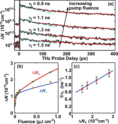
Figure 5(a) shows the change in the mobile carrier density at 45 K for various pump fluences, determined from measured on long time scales ( ps). As expected, the carrier density decays after reaching a peak value in the first few picoseconds after photoexcitation. We attribute this relaxation to carrier trapping and recombination by defects. The carrier density decay rate is relatively fast in the first 100 ps after photoexcitation, after which the decay occurs on much longer time scales. The maximum probe delay allowed by our setup, 400 ps, is unable to resolve these long time scales. But the non-zero carrier densities observed at negative probe delays show that the photoexcited carrier density does not completely decay in the time interval, around 12.3 ns, between two successive optical pulses. The carrier densities immediately before and after photoexcitation, as a function of pump fluence, reveal the carrier density dependence of the long term (100 ps) recombination rates. Figure 5(b) shows the change in carrier density immediately before, , and after, , photoexcitation. Both and increase with the pump fluence in a nonlinear fashion, so carrier-density-independent recombination times can be ruled out. We also estimate the initial recombination rate, , versus pump fluence from the slope of the blue dash-dot lines in Figure 5(a). Figure 5(c) shows that increases approximately linearly with . Any physical model that describes the observed carrier dynamics must account for the transition from the fast decay rates in the first 100 ps to the slow decay rates thereafter. In addition, the model must account for the severe nonlinearity of and versus pump fluence.
Here, we present a model of carrier relaxation based on trapping and recombination by optically-active defect states. This model explains all features of the observed carrier dynamics at 45 K. The natural MoS2 used in our work is known to have defects such as vacancies, grain boundaries, and impuritiesZhou et al. (2013); Zhu et al. (2014). Many of these defects are optically active in the near-IR wavelength region and appear in the optical absorption spectraYuan et al. (2014); Wang et al. (2014, 2013). We assume that the initial fast decay of the photoexcited carrier density is due to the capture of electrons by defect states in the bandgapFurchi et al. (2014) (see Figure 1(b)). As these defect states become full of electrons, the decay rate decreases (due to Pauli blocking) and becomes limited by the capture of photoexcited holes from the valence band. The optical pump pulse excites electrons to the conduction band from both the valence band and also the defect states, and we assume that the defect states become empty immediately after the pump pulseWang et al. (2014, 2013). Our final assumption is that the defect states are assumed to be occupied by electrons in thermal equilibrium in our n-doped sample.
Ignoring thermal generation of electrons and holes from defect states, the rate equations for the decay of the electron and hole densities in our model are (see supplementary information),
| (5) |
Here, and are the total mobile electron and hole densities, respectively, and () is the rate constant for electron capture (hole capture) by the defect states via the dominant Auger mechanisms in a n-doped semiconductorLandsberg (1992). The value is the sum of the equilibrium electron density, , and the excess photoexcited electron density. is the density of defect states, and is the electron occupation of the defect states, assumed to be unity in equilibrium. Note that a phonon-assisted carrier trapping process would not have the carrier density dependence consistent with the observed decay ratesLandsberg (1992). We varied the values of the fitting parameters , , , and in simulations to fit the data in Figures 5(a) and 5(b). The simulations involved time-stepping the rate equations over many (1-5) pump pulse cycles until a steady state was achieved. The difference cm-3 per J cm-2 determined the mobile carrier density created by the pump pulse in our simulations.
The data in Figure 5 can inform the search for appropriate values of the fitting parameters. Immediately after photoexcitation, since varies as , the slope of the line in Figure 5(c) estimates the product . Since the long term decay of the photoexcited density is limited by the capture of holes in defects, the values of estimate the product . Finally, the density of defect states governs how quickly they fill with electrons, therefore is determined from the time at which the initial fast decay transitions to the slower decay, as measured in Figure 5(a). The values of fitting parameters that best fit the data are: cm6 s-1, cm6 s-1, cm-3, and cm-3. This value of corresponds to a DC conductivity of 12 S m-1, which compares well with the value of conductivity obtained from THz transmission measurements of the unpumped sample, S m-1. The model presented here closely agrees with the data, accurately reproducing the values of , the relaxation curves, and the nonlinearity of versus pump fluence.
II Discussion
In this paper, we presented measurements of the mobility of photoexcited carriers in multilayer MoS2 using THz time-domain spectroscopy. The observed temperature dependence of the mobility for K indicates acoustic phonon scattering as the dominant mobility-limiting mechanism. The measured carrier momentum scattering rates are comparable to theoretical predictions based on phonon-scattering-limited transportKaasbjerg et al. (2012); Ma and Jena (2014). In contrast, previously reported DC electrical measurements have suggested impurity or defect scattering as the dominant mobility-limiting mechanism in multilayer MoS2Fivaz and Mooser (1967); Kim et al. (2012); Radisavljevic and Kis (2013); Bao et al. (2013). Given the prevalence of defects and impurities in MoS2Zhou et al. (2013); Zhu et al. (2014), it is intriguing that we observe mobilities limited by acoustic phonon scattering. The observed high mobilities at low temperatures in our experiments could be related to the fact that our measurements were performed at very high frequencies. It is well known theoretically and experimentally that AC conductivity in disordered materials increases with the AC frequencyPollak and Geballe (1961); Rockstad (1970); Pike (1972); Landauer (1952); Clerc et al. (1990); Henning et al. (1999). This phenomenon appears in the microscopic models of hopping conductionPollak and Geballe (1961); Rockstad (1970); Pike (1972) as well as in the classical models of the AC conductivity in inhomogeneous materialsLandauer (1952); Clerc et al. (1990); Henning et al. (1999). Since we did not see signatures of AC hopping conduction in our sample at any temperature, we believe models that describe the AC conductivity in inhomogeneous materials are more relevant to our observationsLandauer (1952); Clerc et al. (1990); Henning et al. (1999). Accordingly, we believe that the MoS2 atomic layers in our sample consist of interspersed high and low mobility regions (due to grain boundaries, crystal defects, impurities, etc.Zhou et al. (2013)) and the conductivity of the layers is determined by the resistive and capacitive couplings of these regionsLandauer (1952); Clerc et al. (1990); Henning et al. (1999). Even a small fraction of low mobility regions can significantly affect the DC conductivity in lower dimensions. The high mobility regions have a conductivity given by the Drude form. The AC conductivity of the sample is then expected to increase with the frequency until the low mobility regions are capacitively shorted out and the conductivity of the sample is then limited by the Drude conductivity of the high mobility regions. Although this model qualitatively explains the observation of the long momentum scattering times in our experiments, investigation of the frequency dependence of the sample conductivity in the low frequency region ( THz) is needed to fully understand the nature of the transport and determine which model, if any, best describes the nature of the conduction.
Carrier relaxation and recombination dynamics directly affect the performance of almost all electronic and optoelectronic devices. We have observed several time scales in the dynamics associated with carrier relaxation and recombination. The initial intraband relaxation (or carrier cooling) occurs within 5 ps. Carrier interband recombination appears to result from carrier trapping in optically active defect states, with recombination lasting over tens of nanoseconds due to slow hole capture in the defect states. It is important to mention that simple bimolecular recombination (proportional to ) and direct interband Auger recombination (proportional to ) are not sufficiently nonlinear to account for the density dependence seen in Figure 5(b). Although our data shows that the recombination times in multilayer MoS2 are long, they are short in comparison with other indirect bandgap semiconductors, such as high-quality Si or Ge, which have recombination times in excess of one microsecond at room temperatureGaubas et al. (2006). We note here that our measurements might not have detected charge trapping dynamics occurring on much longer time scales (10 ns) recently observed in MoS2 photoconductive devicesCho et al. (2014).
The authors would like to acknowledge helpful discussions with Haining Wang, Michael G. Spencer, and Paul L. McEuen, as well as support from CCMR under NSF grant number DMR-1120296, AFOSR-MURI under grant number FA9550-09-1-0705, ONR under grant number N00014-12-1-0072, and the Cornell Center for Nanoscale Systems funded by NSF.
III Methods
III.1 Sample Preparation and Measurements
The multilayer MoS2 sample used in this study was cleaved from a large piece of natural MoS2 (SPI Supplies). We adhered the resulting flake to completely cover a 2 mm clear aperture and mounted the sample in a cryostat. By measuring the broadband optical transmission interference fringes and using existing index of refraction dataEvans and Young (1965), we determined that the average thickness of the flake was 4 m, with variations of m across the aperture. Electron-hole pairs were optically excited in the MoS2 using sub-100 fs pulses from a Ti:Sapphire oscillator with a center frequency of 785 nm, pulse repetition rate of 81 MHz, and maximum fluence of 1.2 J cm-2. We used synchronized, few-cycle THz pulses, generated and detected with photoconductive switches in a THz time-domain spectrometerKatzenellenbogen and Grischkowsky (1991), to probe the excited carrier distribution. Optical pump and THz probe beams were mechanically chopped at 400 and 333 Hz, respectively, and the detected photocurrent was demodulated with a lock-in amplifier at the sum frequency.
III.2 Extraction of from Measurements
The Fourier transform of Equation 3 is,
| (6) |
where, equals . Here, is the Fourier transform operator with respect to . Measurement of enables one to obtain using Equation 2, and then can be obtained using the above Equation. In general, does not equal Nienhuys and Sundström (2005). However, if the DC conductivity is changing slowly compared to the duration of the current impulse response then . Since the carrier density, and therefore the DC conductivity, varies slowly for ps in all of our measurements, we have extracted using this simple relation for ps. But extracting from for cases when the DC conductivity varies rapidly, such as in Figure 4(b), requires two transformationsNienhuys and Sundström (2005): First, , followed by, . These transformations can add considerable noise, and we have employed them only to extract the DC conductivity changes for small pump-probe delays, ps, and low temperatures.
References
- Podzorov et al. (2004) V. Podzorov, M. E. Gershenson, C. Kloc, R. Zeis, and E. Bucher, Applied Physics Letters 84, 3301 (2004), URL http://scitation.aip.org/content/aip/journal/apl/84/17/10.1063/1.1723695.
- Splendiani et al. (2010) A. Splendiani, L. Sun, Y. Zhang, T. Li, J. Kim, C.-Y. Chim, G. Galli, and F. Wang, Nano Letters 10, 1271 (2010), pMID: 20229981, eprint http://pubs.acs.org/doi/pdf/10.1021/nl903868w, URL http://pubs.acs.org/doi/abs/10.1021/nl903868w.
- Mak et al. (2010) K. F. Mak, C. Lee, J. Hone, J. Shan, and T. F. Heinz, Phys. Rev. Lett. 105, 136805 (2010), URL http://link.aps.org/doi/10.1103/PhysRevLett.105.136805.
- Eda et al. (2011) G. Eda, H. Yamaguchi, D. Voiry, T. Fujita, M. Chen, and M. Chhowalla, Nano Letters 11, 5111 (2011), eprint http://pubs.acs.org/doi/pdf/10.1021/nl201874w, URL http://pubs.acs.org/doi/abs/10.1021/nl201874w.
- Yoon et al. (2011) Y. Yoon, K. Ganapathi, and S. Salahuddin, Nano Letters 11, 3768 (2011), eprint http://pubs.acs.org/doi/pdf/10.1021/nl2018178, URL http://pubs.acs.org/doi/abs/10.1021/nl2018178.
- Cao et al. (2012) T. Cao, G. Wang, W. Han, H. Ye, C. Zhu, J. Shi, Q. Niu, P. Tan, E. Wang, B. Liu, et al., Nature Communications 3, 887 (2012), URL http://www.nature.com/ncomms/journal/v3/n6/full/ncomms1882.html.
- Kioseoglou et al. (2012) G. Kioseoglou, A. T. Hanbicki, M. Currie, A. L. Friedman, D. Gunlycke, and B. T. Jonker, Applied Physics Letters 101, 221907 (pages 4) (2012), URL http://link.aip.org/link/?APL/101/221907/1.
- van der Zande et al. (2013) A. M. van der Zande, P. Y. Huang, D. A. Chenet, T. C. Berkelbach, Y. You, G.-H. Lee, T. F. Heinz, D. R. Reichman, D. A. Muller, and J. C. Hone, Nature Materials p. 554 (2013), URL http://www.nature.com/nmat/journal/v12/n6/full/nmat3633.html.
- Zhou et al. (2013) W. Zhou, X. Zou, S. Najmaei, Z. Liu, Y. Shi, J. Kong, J. Lou, P. M. Ajayan, B. I. Yakobson, and J.-C. Idrobo, Nano Letters 13, 2615 (2013), eprint http://pubs.acs.org/doi/pdf/10.1021/nl4007479, URL http://pubs.acs.org/doi/abs/10.1021/nl4007479.
- Wang et al. (2012a) Q. H. Wang, K. Kalantar-Zadeh, A. Kis, J. N. Coleman, and M. S. Strano, Electronics and optoelectronics of two-dimensional transition metal dichalcogenides (2012a), URL http://www.nature.com/nnano/journal/v7/n11/full/nnano.2012.193.html.
- Wang et al. (2012b) H. Wang, L. Yu, Y.-H. Lee, Y. Shi, A. Hsu, M. L. Chin, L.-J. Li, M. Dubey, J. Kong, and T. Palacios, Nano Letters 12, 4674 (2012b), eprint http://pubs.acs.org/doi/pdf/10.1021/nl302015v, URL http://pubs.acs.org/doi/abs/10.1021/nl302015v.
- Laskar et al. (2013) M. R. Laskar, L. Ma, S. Kannappan, P. Sung Park, S. Krishnamoorthy, D. N. Nath, W. Lu, Y. Wu, and S. Rajan, Applied Physics Letters 102, 252108 (2013), URL http://scitation.aip.org/content/aip/journal/apl/102/25/10.1063/1.4811410.
- Lopez-Sanchez et al. (2013) O. Lopez-Sanchez, D. Lembke, M. Kayci, A. Radenovic, and A. Kis, Nature Nanotechnology 8, 497 (2013), URL http://www.nature.com/nnano/journal/v8/n7/full/nnano.2013.100.html.
- Perkins et al. (2013) F. K. Perkins, A. L. Friedman, E. Cobas, P. M. Campbell, G. G. Jernigan, and B. T. Jonker, Nano Letters 13, 668 (2013), eprint http://pubs.acs.org/doi/pdf/10.1021/nl3043079, URL http://pubs.acs.org/doi/abs/10.1021/nl3043079.
- Malard et al. (2013) L. M. Malard, T. V. Alencar, A. P. M. Barboza, K. F. Mak, and A. M. de Paula, Phys. Rev. B 87, 201401 (2013), URL http://link.aps.org/doi/10.1103/PhysRevB.87.201401.
- Zhu et al. (2014) W. Zhu, T. Low, Y.-H. Lee, H. Wang, D. B. Farmer, J. Kong, F. Xia, and P. Avouris, Nature Communications 5, 4087 (2014), URL http://www.nature.com/ncomms/2014/140117/ncomms4087/full/ncomms4087.html.
- Mak (2014) (2014), URL http://arxiv.org/abs/1403.5039.
- Das et al. (2013) S. Das, H.-Y. Chen, A. V. Penumatcha, and J. Appenzeller, Nano Letters 13, 100 (2013), eprint http://pubs.acs.org/doi/pdf/10.1021/nl303583v, URL http://pubs.acs.org/doi/abs/10.1021/nl303583v.
- Bao et al. (2013) W. Bao, X. Cai, D. Kim, K. Sridhara, and M. S. Fuhrer, Applied Physics Letters 102, 042104 (pages 4) (2013), URL http://link.aip.org/link/?APL/102/042104/1.
- Fivaz and Mooser (1967) R. Fivaz and E. Mooser, Phys. Rev. 163, 743 (1967), URL http://link.aps.org/doi/10.1103/PhysRev.163.743.
- Kim et al. (2012) S. Kim, A. Konar, W.-S. Hwang, J. H. Lee, J. Lee, J. Yang, C. Jung, H. Kim, and J.-Y. Yoo, Ji-Beom ang Choi, Nature Communications p. 1011 (2012), URL http://www.nature.com/ncomms/journal/v3/n8/full/ncomms2018.html.
- Pradhan et al. (2013) N. R. Pradhan, D. Rhodes, Q. Zhang, S. Talapatra, M. Terrones, P. M. Ajayan, and L. Balicas, Applied Physics Letters 102, 123105 (pages 4) (2013), URL http://link.aip.org/link/?APL/102/123105/1.
- Radisavljevic and Kis (2013) B. Radisavljevic and A. Kis, Nature Materials p. 815–820 (2013), URL http://www.nature.com/nmat/journal/v12/n9/full/nmat3687.html.
- Kumar et al. (2013) N. Kumar, J. He, D. He, Y. Wang, and H. Zhao, Journal of Applied Physics 113, 133702 (pages 6) (2013), URL http://link.aip.org/link/?JAP/113/133702/1.
- Kaasbjerg et al. (2012) K. Kaasbjerg, K. S. Thygesen, and K. W. Jacobsen, Phys. Rev. B 85, 115317 (2012), URL http://link.aps.org/doi/10.1103/PhysRevB.85.115317.
- Ma and Jena (2014) N. Ma and D. Jena, Phys. Rev. X 4, 011043 (2014), URL http://link.aps.org/doi/10.1103/PhysRevX.4.011043.
- Korn et al. (2011) T. Korn, S. Heydrich, M. Hirmer, J. Schmutzler, and C. Schuller, Applied Physics Letters 99, 102109 (pages 3) (2011), URL http://link.aip.org/link/?APL/99/102109/1.
- Katzenellenbogen and Grischkowsky (1991) N. Katzenellenbogen and D. Grischkowsky, Appl. Phys. Lett. 58, 222 (1991).
- Zhang et al. (2014) C. Zhang, H. Wang, W. Chan, C. Manolatou, and F. Rana, Phys. Rev. B 89, 205436 (2014), URL http://link.aps.org/doi/10.1103/PhysRevB.89.205436.
- Kindt and Schmuttenmaer (1999) J. T. Kindt and C. A. Schmuttenmaer, The Journal of Chemical Physics 110, 8589 (1999), URL http://link.aip.org/link/?JCP/110/8589/1.
- Beard et al. (2000) M. C. Beard, G. M. Turner, and C. A. Schmuttenmaer, Phys. Rev. B 62, 15764 (2000), URL http://link.aps.org/doi/10.1103/PhysRevB.62.15764.
- Nienhuys and Sundström (2005) H.-K. Nienhuys and V. Sundström, Phys. Rev. B 71, 235110 (2005), URL http://link.aps.org/doi/10.1103/PhysRevB.71.235110.
- Jnawali et al. (2013) G. Jnawali, Y. Rao, H. Yan, and T. F. Heinz, Nano Letters 13, 524 (2013), eprint http://pubs.acs.org/doi/pdf/10.1021/nl303988q, URL http://pubs.acs.org/doi/abs/10.1021/nl303988q.
- Peelaers and Van de Walle (2012) H. Peelaers and C. G. Van de Walle, Phys. Rev. B 86, 241401 (2012), URL http://link.aps.org/doi/10.1103/PhysRevB.86.241401.
- Zahid et al. (2013) F. Zahid, L. Liu, Y. Zhu, J. Wang, and H. Guo, AIP Advances 3, 052111 (pages 6) (2013), URL http://link.aip.org/link/?ADV/3/052111/1.
- Kawamura and Das Sarma (1992) T. Kawamura and S. Das Sarma, Phys. Rev. B 45, 3612 (1992), URL http://link.aps.org/doi/10.1103/PhysRevB.45.3612.
- Cheiwchanchamnangij and Lambrecht (2012) T. Cheiwchanchamnangij and W. R. L. Lambrecht, Phys. Rev. B 84, 205302 (2012).
- Feng et al. (2012) J. Feng, X. Qian, C.-W. Huang, and J. Li, Nature Photonics 6, 866 (2012).
- He et al. (2013) K. He, C. Poole, K. F. Mak, and J. Shan, Nano Letters 13, 2931 (2013).
- Wang et al. (2010) H. Wang, J. H. Strait, P. A. George, S. Shivaraman, V. B. Shields, M. Chandrashekhar, J. Hwang, F. Rana, M. G. Spencer, C. S. Ruiz-Vargas, et al., Applied Physics Letters 96, 081917 (2010), URL http://scitation.aip.org/content/aip/journal/apl/96/8/10.1063/1.3291615.
- Lundstorm (2009) M. Lundstorm, Fundamentals of Carrier Transport (Cambridge University Press, cambridge, UK, 2009), 2nd ed.
- Yuan et al. (2014) S. Yuan, R. Roldán, M. I. Katsnelson, and F. Guinea, Phys. Rev. B 90, 041402 (2014), URL http://link.aps.org/doi/10.1103/PhysRevB.90.041402.
- Wang et al. (2014) S. Wang, H. Yu, H. Zhang, A. Wang, M. Zhao, Y. Chen, L. Mei, and J. Wang, Advanced Materials 26, 3538 (2014), ISSN 1521-4095, URL http://dx.doi.org/10.1002/adma.201306322.
- Wang et al. (2013) K. Wang, J. Wang, J. Fan, M. Lotya, A. O’Neill, D. Fox, Y. Feng, X. Zhang, B. Jiang, Q. Zhao, et al., ACS Nano 7, 9260 (2013), eprint http://pubs.acs.org/doi/pdf/10.1021/nn403886t, URL http://pubs.acs.org/doi/abs/10.1021/nn403886t.
- Furchi et al. (2014) M. M. Furchi, D. K. Polyushkin, A. Pospischil, and T. Mueller, arXiv:1406.5640 (2014), URL http://arxiv.org/abs/1406.5640.
- Landsberg (1992) P. T. Landsberg, Recombination in Semiconductors (Cambridge University Press, cambridge, UK, 1992), 1st ed.
- Pollak and Geballe (1961) M. Pollak and T. H. Geballe, Phys. Rev. 122, 1742 (1961), URL http://link.aps.org/doi/10.1103/PhysRev.122.1742.
- Rockstad (1970) H. K. Rockstad, Journal of Non-Crystalline Solids pp. 192–202 (1970).
- Pike (1972) G. E. Pike, Phys. Rev. B 6, 1572 (1972), URL http://link.aps.org/doi/10.1103/PhysRevB.6.1572.
- Landauer (1952) R. Landauer, Journal of Applied Physics 23, 779 (1952), URL http://scitation.aip.org/content/aip/journal/jap/23/7/10.1063/1.1702301.
- Clerc et al. (1990) J. Clerc, G. Giraud, J. Laugier, and J. Luck, Advances in Physics 39, 191 (1990), eprint http://dx.doi.org/10.1080/00018739000101501, URL http://dx.doi.org/10.1080/00018739000101501.
- Henning et al. (1999) P. F. Henning, C. C. Homes, S. Maslov, G. L. Carr, D. N. Basov, B. Nikolić, and M. Strongin, Phys. Rev. Lett. 83, 4880 (1999), URL http://link.aps.org/doi/10.1103/PhysRevLett.83.4880.
- Gaubas et al. (2006) E. Gaubas, M. Bauža, A. Uleckas, and J. Vanhellenmont, Mat. Sci. in Semicond. Proc. 9, 781 (2006).
- Cho et al. (2014) K. Cho, T.-Y. Kim, W. Park, J. Park, D. Kim, J. Jang, H. Jeong, S. Hong, and T. Lee, Nanotechnology 25, 155201 (2014), URL http://iopscience.iop.org/0957-4484/25/15/155201/.
- Evans and Young (1965) B. L. Evans and P. A. Young, Proceedings of the Royal Society of London. Series A. Mathematical and Physical Sciences 284, 402 (1965), eprint http://rspa.royalsocietypublishing.org/content/284/1398/402.full.pdf+html, URL http://rspa.royalsocietypublishing.org/content/284/1398/402.abstract.
- Ridley (2013) B. K. Ridley, Quantum Processes in Semiconductors (Oxford University Press, New York, USA, 2013), 5th ed.
IV Supplementary Information for “High Intrinsic Mobility and Ultrafast Carrier Dynamics in Multilayer Metal Dichalcogenide MoS2”
IV.1 Expressions for the transmission of THz pulses
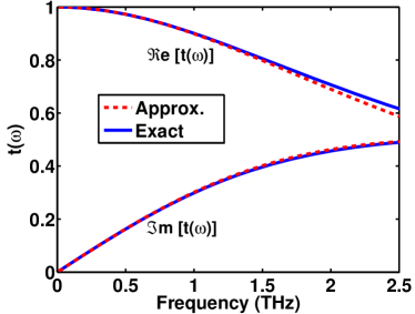
We use Equation 1 of the main text to estimate the frequency-dependent transmission of THz pulses through the MoS2 sample. Equation 1 can be derived as follows. We start with the exact solution for the transmission of light through an etalon with a refractive index and thickness , surrounded by air (),
| (7) |
In the limit, ,
| (8) |
For the measured THz refractive index of MoS2, , and the thickness of our sample, m, the approximation in the above expression is extremely good, as illustrated in Figure 6.
In the case of a conductive medium, with conductivity , the complex refractive index is, . Here, is the frequency-independent refractive index and is the permittivity of free space. The inverse Fourier transform of the relation in Equation 8 gives,
| (9) |
Subtracting versions of the above equation in the presence and absence of optical pumping one obtains,
| (10) |
Equation 2 in the text follows directly from the above relation following the substitution .
IV.2 Derivation of Equation 3 in the Main Text
In this Section, we wish to establish Equations 3 and 6 of the main text. We assume that the current density in the sample for pump-probe delay in the presence of the field of a THz pulse and a time-dependent DC conductivity isNienhuys and Sundström (2005),
| (11) |
Here, is the normalized current impulse response () and is the convolution operator with respect to . This is the most general way of writing the current response if the current density obeys the operator equation,
| (12) |
where, is a linear-time-invariant (LTI) differential operator. Equation 11 gives,
| (13) |
The change in the current density in the presence and absence of pumping is . Here, the subscripts p and 0 indicate the value with and without optical pumping, respectively. Therefore, one obtains,
| (14) |
By applying a Fourier transform with respect to to each term, we have,
| (15) |
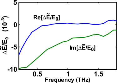
Equations 3 and 6 of the main text will be valid provided the final two terms on the right hand side of Equation 15 are negligibly small compared to the first term. In Figure 7, we show a representative measured ratio of , which is at most on the order of for the highest pump fluence used in our experiments. At all other temperatures, pump fluences, and pump-probe delays, this ratio is either similar or smaller. Since at all frequencies, we can safely neglect compared to in Equation 15. Next, using Equation 2 from the main text, we see that the ratio S m-1. In contrast, the measured value of the unpumped DC conductivity is smaller than S m-1 and, therefore, at all frequencies. Consequently, we can also neglect compared to in Equation 15. In this way, we empirically verify that our use of the approximations in Equations 3 and 6 in the main text is valid for our our experiments. Theoretically, it can be shown that,
| (16) |
The second term in Equation 15 can be neglected provided , which is indeed the case in our experiments.
IV.3 Model for electron-hole recombination via mid-gap defect states
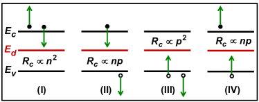
There are essentially two main mechanisms for the capture/emission of electrons and holes at/from localized crystal defectsLandsberg (1992): (1) Phonon-assisted processes, and (2) Auger processes. Phonon-assisted processes can be single-phonon processes or multi-phonon processes, including phonon-cascade processesRidley (2013). In phonon-assisted processes the capture rates (units: cm-3s-1), tend to go linearly with the carrier density (i.e. the capture times are independent of the carrier density). The capture times observed in our experiments are carrier density dependent (inverse electron capture times increase linearly with the electron density), as shown in Figure 5(c) of the main text. The capture times in Auger processes are carrier density dependent. Figure 8 shows the four basic Auger processes for the capture of electrons ((I) and (II)) and holes ((III) and (IV)) at defects. The corresponding emission processes are the just the inverse of the capture processes. The rate equations for each Auger process (and its inverse) can be written using Figure 8. For example, the electron density rate equation for process (I) and its inverse is,
| (17) |
Here, is the electron density, is the rate constant for electron capture by the defect state, is the defect density, and is the occupation of the defect state. The first terms describes the capture process and the second term describes the emission process. The value of the constant can be determined by using the fact that in thermal equilibrium :
| (18) |
where is the equilibrium electron density and is the equilibrium defect occupation. If in equilibrium , as is expected for defects deeper than a few in an n-doped material, then can be assumed to be negligibly small and electron generation from the defect states can be ignored in the above equation. Process (I) and process (II) can have comparable magnitudesLandsberg (1992). So, ignoring emission processes, the rate equation for the electron density becomes,
| (19) |
and are the rate constants for electron capture by the defect state corresponding to processes (I) and (II) in Figure 8, respectively. In our experiments, since our MoS2 sample is n-doped, the first term of the right hand side is more important for small pump fluence values (when the hole density is small) compared to the second term. For large pump fluence values, both the electron and the hole densities can become comparable and the second term on the right hand side may not be ignored. However, at large pump fluences the effect of the second term is indistinguishable from the first term in our pump-probe experiments (since both terms would result in the inverse electron capture time to increase linearly with the photoexcited carrier density). Since the pump fluences used in our experiments are relatively small (and the maximum photoexcited carrier density is in the low cm-3), we have chosen to ignore the second term, corresponding to process (II), in the above Equation for simplicity. Similarly, ignoring emission processes, the rate equation for the hole density becomes,
| (20) |
Here, is the hole density. and are the rate constants for hole capture by the defect state corresponding to processes (III) and (IV) in Figure 8, respectively. Again, since our MoS2 sample is n-doped and the pump fluences used in our experiments are small, we have chosen to ignore the second term, corresponding to process (IV), in the above Equation for simplicity.