Graphene Versus MoS2: a Mini Review
Abstract
Graphene and MoS2 are two well-known quasi two-dimensional materials. This review is a comparative survey of the complementary lattice dynamical and mechanical properties of graphene and MoS2. This comparison facilitates the study of graphene/MoS2 heterostructures, which is expected to mitigate the negative properties of each individual constituent.
pacs:
68.65.-k, 63.22.-m, 62.20.-xI Introduction
Quasi two-dimensional (Q2D) materials have many novel properties and have attracted intensive research interest over the past decades. The size of the family of Q2D materials keeps expanding. The Q2D family currently contains the following materials: graphene, hexagonal boron nitride, 2D honeycomb silicon, layered transition metal dichalcogenides (MoS2, WS2, …), black phosphorus and 2D ZnO. Graphene is the most well-known material among the Q2D family of materials. Novoselov and Geim were awarded the Nobel prize in physics for graphene in 2010.Geim and Novoselov (2007)
The investigations on graphene are extensive but not exhaustive.Neto and Novoselov (2011) They are helpful for the whole Q2D family because many of the experimental set ups (initially for graphene) can be used to perform measurements on other materials in this family. For example, the mechanical properties of single-layer MoS2 (SLMoS2) were successfully measured using the same nanoindentation platform as graphene.Lee et al. (2008); Cooper et al. (2013a) In the theoretical community, many theorems or approaches, initially developed to study graphene, are also applicable to other Q2D materials. Some of the extensions may turn out to be trivial because of the common two-dimensional nature of these materials. However, the extensions may bring about new findings as these Q2D materials have different microscopic structures. For example, the bending modulus of SLMoS2 can be derived using a similar analytic approach as graphene. The bending modulus of SLMoS2 is about seven times larger than that of graphene, owing to its trilayer structure (one Mo layer sandwiched between two S layers).Ou-Yang. et al. (1997); Tu and Ou-Yang (2002); Arroyo and Belytschko (2001); Lu et al. (2009); Jiang et al. (2013a) Another example is the puckered micro structure of black phosphorus, which leads to a negative Poisson’s ratio in the out-of-plane direction.Jiang and Park (2014a)
From the above, we found that graphene is attracting ongoing research interest from both the academic and applied communities. Many review articles have been devoted to graphene. Geim and Novoselov (2007); Ferrari (2007); Castro Neto et al. (2009); Geim (2009); Malard et al. (2009); Rao et al. (2009); Allen et al. (2010); Bonaccorso et al. (2010); Schwierz (2010); Balandin (2011) Addition, more and more researchers have begun examining possible applications of other Q2D materials, using the knowledge gained from graphene. In particular, MoS2 has attracted considerable research interest. Many review articles have also been published on MoS2.Wang et al. (2012a); Chhowalla et al. (2013); Xu et al. (2013); Butler et al. (2013); Huang et al. (2013a)
The present review focusses on a detailed comparison of the mechanical properties of graphene and SLMoS2. This comparison makes it clear as to what the positive/negative properties for graphene and MoS2 are, highlighting the possible advanced features and drawbacks of graphene/MoS2 heterostructures.Britnell et al. (2013) These heterostructures were expected to mitigate the negative properties of each individual constituent. For example, graphene/MoS2/graphene heterostructures have efficient photon absorption and electron-hole creation properties, because of the enhanced light-matter interactions in the SLMoS2 layer.Britnell et al. (2013) Another experiment recently showed that MoS2 can be protected from radiation damage by coating it with graphene layers.Zan et al. (2013) This design exploits the outstanding mechanical properties of graphene.
In this review, we introduce and compare the following properties for graphene and the SLMoS2; the structure, interatomic potential, phonon dispersion, Young’s modulus, yield stress, bending modulus, buckling phenomenon, nanomechanical resonator, thermal conductivity, electronic band structure, optical absorption, and the graphene/MoS2 heterostructure. This article ends up with a table that lists the major results for all of the properties that are compared in the article.
II Structure and Interatomic Potential
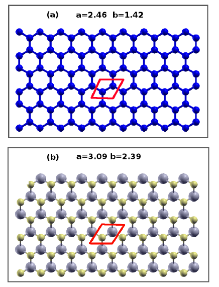
Structure. First, the structures of graphene and SLMoS2 are compared. Fig. 1 (a) shows that graphene has a honeycomb lattice structure with a point group. There are two inequivalent carbon atoms in the unit cell. These two carbon atoms are reflected onto each other by the inverse symmetry operation from the point group. The lattice constant is Å and the C-C bond length is Å.Saito et al. (1998)
Figure 1 (b) shows the top view of the SLMoS2 structure. SLMoS2 has a trilayer structure with one Mo atomic layer sandwiched between two outer S atomic layers. The small yellow balls represent the projection of the outer two S atomic layers onto the Mo atomic layer. The point group for SLMoS2 is . The rotation symmetry is broken in SLMoS2. There are two S atoms and one Mo atom in the unit cell. The lattice constant for the in-plane unit cell is Å and the Mo-S bond length is Å. These values were computed using the Stillinger-Weber (SW) potential.Jiang et al. (2013b) They agree with the first-principles calculationsMolina-Sánchez and Wirtz (2011) and the experiments.Wakabayashi et al. (1975)
Interatomic potential. The interactions between the carbon atoms in graphene can be calculated using four different computation cost levels. The first principles calculation is the most expensive approach to compute the interatomic energy of graphene. Many existing simulation packages can be used for such calculations, including the commercial Vienna Ab-initio Simulation Package (VASP)Kresse and Furthmuller (1996) and the freely available Spanish Initiative for Electronic Simulations with Thousands of Atoms (SIESTA) package.Soler et al. (2002) To save on the computation cost, Brenner et al. developed an empirical potential for carbon-based materials, including graphene.Brenner et al. (2002) The Brenner potential takes the form of the bond-order Tersoff potentialTersoff (1988) and is able to capture most of the linear properties and many of the nonlinear properties of graphene. For instance, it can describe the formation and breakage of bonds in graphene, providing a good description of its structural, mechanical and thermal properties. The Tersoff potentialTersoff (1988) or the SW potentialStillinger and Weber (1985); Abraham and Batra (1989) provides reasonable predictions for some of the nonlinear and linear properties of graphene. These two empirical potentials have fewer parameters than the Brenner potential, thus they are faster than the Brenner potential. Last, the linear part of the C-C interactions in graphene can be captured using valence force field models (VFFMs).Aizawa et al. (1990) The VFFMs have the most inexpensive computation cost and can be used to efficiently compute some of the linear properties.
The potentials of these four computation levels can also be used for SLMoS2. First principles calculations can also be used for SLMoS2. In 2009, Liang et al. parameterized a bond-order potential for SLMoS2,Liang et al. (2009) which was based on the bond order concept underlying the Brenner potential.Brenner et al. (2002) This Brenner-like potential was recently further modified to study the nanoindentations in SLMoS2 thin films using a molecular statics approach.Stewart and Spearot (2013) Recently, we parameterized the SW potential for SLMoS2, where potential parameters were fitted to the phonon spectrum.Jiang et al. (2013b) This potential could easily be used in some of the popular simulation packages, such as the General Utility Lattice Program (GULP)Gale (1997) and the Large-Scale Atomic/Molecular Massively Parallel Simulator (LAMMPS).Lammps (2012) In 1975, Wakabayashi et al.Wakabayashi et al. (1975) developed a VFFM to calculate the phonon spectrum in bulk MoS2. This linear model has been used to study the lattice dynamical properties of some MoS2 based materials.Jimenez Sandoval et al. (1991); Dobardzic et al. (2006); Damnjanovic et al. (2008)
III Phonon Dispersion
A phonon is a quasiparticle in reciprocal space. Each phonon mode describes a particular type of collective vibrations for all of the atoms in the real lattice space. The symmetry of the vibration morphology follows an irreducible representation of the space group of the system. These irreducible representations are denoted by the wave vector . The phonon modes are denoted by the wave vector and the branch index , where is the inter-cell degree of freedom and corresponds to the intra-cell degree of freedom. Each phonon mode has a specific angular frequency () and eigenvector (). For graphene and SLMoS2, each degree of freedom in the real lattice space can be indicated as . and denote the position of the unit cell. describes the different atoms in the unit cell and is the direction of the axis. The frequency and the eigenvector of the phonon mode can be obtained through the diagonalization of the following dynamical matrix,
The force constant matrix stores the information on the interactions between the two degrees of freedom, () and (). gives the total number of unit cells. For the short-range interactions, a summation over can be truncated to the summation over the neighboring atoms.
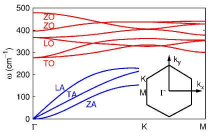
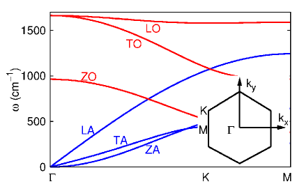
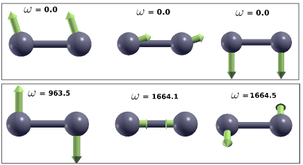
Figure 2 shows the phonon dispersion of graphene along the high symmetry KM lines in the first Brillouin zone. The force constant matrix was constructed using the Brenner potential.Brenner et al. (2002) The inset shows the first Brillouin zone for the hexagonal lattice structure. There are six phonon branches in graphene according to the two inequivalent carbon atoms in the unit cell. These branches (from bottom to top) are the z-directional acoustic (ZA), transverse acoustic (TA), longitudinal acoustic (LA), z-directional optical (ZO), transverse optical (TO), and longitudinal optical (LO) branches. The three blue curves in the lower frequency range correspond to the three acoustic branches, while the upper three red curves correspond to the optical branches. The eigenvectors of the six phonon modes at the point in the first Brillouin zone of graphene are displayed in Fig. 3. In the top panel, the three acoustic phonon modes have zero frequency, indicating that the interatomic potential did not vary during the rigid translational motion. In the bottom panel, the two in-plane optical phonon modes have almost the same frequency, revealing the isotropic phonon properties for the two in-plane directions in graphene.Wang et al. (2009a)
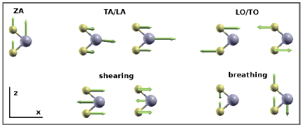
Figure 4 shows the phonon dispersion of SLMoS2 along the high symmetry KM lines in the first Brillouin zone. The atomic interactions are described by the SW potential.Jiang et al. (2013b) The inset shows the same first Brillouin zone as graphene. Each unit cell has one Mo atom and two S atoms, thus there are nine branches in the phonon spectrum. The three lower blue curves correspond to the three acoustic branches, while the six upper curves correspond to the optical branches. Fig. 5 shows the eigenvectors for the nine phonons at the point in the first Brillouin zone of SLMoS2. There are two interesting shear-like phonon modes and two inter-layer breathing-like phonon modes, as shown in the second raw.Zhang et al. (2013a)
From the phonon dispersion of graphene and SLMoS2, it is difficult to determine which material has better phonon properties. Yet, there are two obvious differences in their phonon dispersions. First, the spectrum of graphene is overall higher than that of SLMoS2 by about a factor of three. As a result, the phonon modes in graphene can carry more energy than those in SLMoS2 in the thermal transport phenomenon, leading to the stronger thermal transport ability of graphene. Second, there is a distinct energy band gap between the acoustic and optical branches in SLMoS2. This band gap forbids many phonon-phonon scattering channels; thus it protects the acoustic phonon modes from being interrupted by the high-frequency optical phonons in SLMoS2.Jiang et al. (2013c) As a result, SLMoS2 nanoresonators have a higher quality (Q)-factor than graphene, since the resonant oscillations in SLMoS2 (related to the ZA mode) are affected by weaker thermal vibrations.
IV Mechanical Properties
The mechanical properties for both graphene and SLMoS2 have been extensively investigated.Huang et al. (2006); Liu et al. (2007); Ni et al. (2009); Gao and Hao (2009); Guo et al. (2010); Shen et al. (2010); Hao et al. (2011); Zheng et al. (2011); Han et al. (2011); Wei et al. (2012); Zhang and Pan (2012); Xu et al. (2012); Yue et al. (2012) Here, several of the basic mechanical properties, including the Young’s modulus, yield stress, bending modulus and buckling phenomenon will be discussed. These mechanical properties are fundamental for the application of graphene or SLMoS2 in nano-devices. A good mechanical stability is essential in nanoscale devices, as they are sensitive to external perturbations because of their high surface to volume ratio.
Young’s modulus. Here, the effective Young’s modulus (), which is thickness independent, is discussed. The Young’s modulus is related to this quantity through , where is the film thickness. The thicknesses were chosen to be 3.35 Å and 6.09 Å for graphene and SLMoS2, respectively. The nanoindentation experiments measured the effective Young’s modulus of graphene to be around 335.0 Nm-1.Lee et al. (2008) This value could be reproduced using a simple approach, in which the nonlinear interactions are estimated from the Tersoff-Brenner potential.Jiang et al. (2010a)
For SLMoS2, similar nanoindentation experiments obtained an average value for the effective Young’s modulus of Nm-1 in the experiment by Bertolazzi et al.,Bertolazzi et al. (2011) and Nm-1, measured by Cooper et al.Cooper et al. (2013a, b) Recently, Liu et al. performed similar nanoindentation experiments on chemical vapor deposited SLMoS2, obtaining an effective Young’s modulus of about 170 Nm-1.Liu et al. (2014) The nanoindentation set up has also been used to study the Young’s modulus of thicker MoS2 films.Castellanos-Gomez et al. (2012) The theoretical prediction of the effective Young’s modulus is 139.5 Nm-1 for SLMoS2, based on the SW potential.Jiang et al. (2013b)
Yield stress. The nanoindentation measurements can also determine the yield stress (, the maximum of the stress-strain curve). Lee et al. determined the yield stress to be Nm-1 for graphene.Lee et al. (2008) The yield stresses obtained with the continuum elasticity theory were 42.4 Nm-1 using a tight-binding atomistic model,Cadelano et al. (2009) and 44.4 Nm-1 using the Brenner potential.Reddy et al. (2006) While the elasticity continuum simulation gave an isotropic value for the yield stress in graphene, microscopic atomic models have predicted the yield stress to be chirality dependent in graphene. The first-principles calculations predicted the yield stress to be 40.5 Nm-1 in the zigzag direction and 36.9 Nm-1 in the armchair direction in graphene.Liu et al. (2007) Molecular mechanics simulations obtained a yield stress of 36.9 Nm-1 in the zigzag direction and 30.2 Nm-1 in the armchair direction in graphene.Zhao et al. (2009) Both of the atomic models showed that graphene has a higher yield stress in the zigzag direction than in the armchair direction. Note that the definition of the armchair/zigzag direction is the opposite in Refs. Liu et al., 2007 and Zhao et al., 2009. We have retained the definition from Ref. Zhao et al., 2009, where the armchair direction is along the direction of the carbon-carbon bonds.
In SLMoS2, nanoindentation experiments found that the yield stress was Nm-1, determined by Bertolazzi et al.,Bertolazzi et al. (2011) and Nm-1, determined by Cooper et al.Cooper et al. (2013a, b) In the first-principles calculations, the yield stress was predicted to be 17.5 Nm-1 under a biaxial strain in SLMoS2.Tao et al. (2014) While the work on the yield stress in SLMoS2 is limited at the present stage, considerable attention has been paid to the novel structure transition in SLMoS2.Lin et al. (2014); Jiang (2014a); Kan et al. (2014); Dang et al. (2014) In this structure transition, the outer two S atomic layers are shifted relative to each other, leading to abrupt changes in the electronic and phonon properties in SLMoS2. This structure transition is the result of the trilayer configuration of SLMoS2 and is not observed in graphene.
Bending modulus. Graphene is extremely soft in the out-of-plane direction, owing to its one-atom-thick structure.Xin et al. (2000); Ma et al. (2011a); Shen and Wu (2012); Shi et al. (2012); Wei et al. (2013) Graphene is so thin that it has an extremely small bending modulus, which can be explained by the well-known relationship in the shell theorem, , where is the thickness and is Poisson’s ratio. The bending modulus of graphene has been derived analytically from two equivalent approaches; it was 1.17 eV using the geometric approach with the interactions described by the VFFM,Ou-Yang. et al. (1997); Tu and Ou-Yang (2002) and 1.4 eV from the exponential Cauchy-Born rule using the Brenner potential.Arroyo and Belytschko (2001); Lu et al. (2009) Note that these two approaches are equivalent to each other and the difference in the bending modulus mainly comes from the different potentials used in these two studies.
A similar analytic approach was used to derive the bending modulus of SLMoS2 using the SW potential.Jiang et al. (2013a) The bending modulus of SLMoS2 is 9.61 eV, which is larger than that of graphene by a factor of seven. The large bending modulus of SLMoS2 is due to its trilayer atomic structure, which results in more interaction terms inhibiting the bending motion. The bending modulus can be calculated using:
| (1) |
where is the bending energy density and is the bending curvature. For SLMoS2, the bending energy can be written as:Jiang et al. (2013a)
| (2) |
where and are the geometrical parameters in the empirical potential expressions. This formula is substantially different from the bending modulus formula for graphene.Arroyo and Belytschko (2004) Specifically, the first derivatives, and , are nonzero, owing to the trilayer structure of SLMoS2. As a result, the bending motion in SLMoS2 will counteract with an increasing amount of cross-plane interactions.
Buckling phenomenon. The buckling phenomenon can be a disaster in electronic devices, but it can also be useful in some situations.Zhang et al. (2010); Wang et al. (2011a); Shi et al. (2011); Wang et al. (2013a) The Euler buckling theorem states that the buckling critical strain can be determined from the effective Young’s modulus and the bending modulus through following formula:Timoshenko and Woinowsky-Krieger (1987)
| (3) |
where is the length of the system. For graphene, Nm-1 and eV, found from the above discussions, giving the explicit formula for the buckling critical strain:
| (4) |
The length () has units of Å.
For SLMoS2, Nm-1 and eV were determined from the above discussions. The explicit formula for the buckling critical strain can is:
| (5) |
The buckling critical strain for SLMoS2 is twenty times larger than graphene, for samples of the same length; i.e., it is difficult to buckle SLMoS2 under external compression. This phenomenon has been examined with both MD simulations and phonon analysis.Jiang (2014a, b)
We have discussed and compared the mechanical properties of graphene and SLMoS2. Graphene has a larger Young’s modulus and a larger yield stress and is more flexible than SLMoS2. However, SLMoS2 has a higher bending modulus and does not buckle as readily under external compression as graphene. Hence, in terms of the mechanical properties, it is more advantageous for graphene and SLMoS2 to be used together in a heterostructure, to mitigate the negative mechanical properties of each constitute.
V Nanomechanical Resonators
Nanoresonators based on two-dimensional materials such as graphene and SLMoS2 are promising candidates for ultra-sensitive mass sensing and detection because of their large surface areas and small masses.He et al. (2005); Zhou et al. (2009); Xu et al. (2010); Liu et al. (2011); Wang et al. (2011b); Xu et al. (2011); Gu et al. (2011); Shen et al. (2012); Zhou et al. (2014) For sensing applications, it is important that the nanoresonator exhibits a high Q-factor because the sensitivity of a nanoresonator is inversely proportional to its Q-factor.Ekinci and Roukes (2005) The Q-factor is a quantity that records the total number of oscillation cycles of the resonator before its resonant oscillation decays considerably. Hence, a weaker energy dissipation leads to a higher Q-factor.
For graphene nanoresonators, the Q-factor increases exponentially with a decreasing temperaturevan der Zande et al. (2010); Chen et al. (2009), . Zande et al.van der Zande et al. (2010) found that the exponent = for temperatures below 40 K. For temperatures above 40 K, . Chen et al.Chen et al. (2009) observed a similar transition in the Q-factor. This continuous transition for the temperature dependence of the Q-factor is attributed to the diffusion of adsorbs in the out-of-plane direction on the surface of the graphene layer.Jiang et al. (2014); Edblom and Isacsson (2014) The MD simulations also predicted a discontinuous transition in the Q-factor at the low temperature of 7.0 K, caused by the in-plane diffusion of adsorbs on the graphene surface.Jiang et al. (2014) A very high Q-factor has been achieved in the laboratory at low temperatures. Bunch et al. observed a Q-factor of 9000 for a graphene nanoresonator at 10 K. van der Zande et al. (2010). Chen et al. also found that the Q-factor increased with decreasing temperature, reaching at 5 K Chen et al. (2009). Eichler et al. Eichler et al. (2011) found that the Q-factor of a graphene nanoresonator reached at 90 mK.
For SLMoS2, two recent experiments demonstrated the nanomechanical resonant behavior in SLMoS2Castellanos-Gomez et al. (2013) and few-layer MoS2Lee et al. (2013). Castellanos-Gomez et al. found that the figure of merit, i.e., the frequency-Q-factor product is Hz for SLMoS2.Castellanos-Gomez et al. (2013) Lee et al. found that few-layer MoS2 resonators exhibit a high figure of merit of Hz.Lee et al. (2013) The high Q-factor of SLMoS2 was attributed to the energy band gap in the phonon dispersion of SLMoS2, which protects the resonant oscillations from being scattered by thermal vibrations.Jiang et al. (2013c) As a result, it was predicted that the Q-factor of SLMoS2 nanoresonators will be higher than the graphene nanoresonators by at least a factor of four.
Although it has been theoretically predicted that MoS2 will have better mechanical resonance behavior than graphene, experiments on MoS2 nanoresonators are limited. More measurements are needed to examine their properties, such as the mass sensitivity. Furthermore, the sensor application of the nanoresonators depends on the level of low frequency 1/f noise, which is a limiting factor for the communication applications and the sensor sensitivity and selectivity for the graphene and MoS2 nanoresonators.Lin and Avouris (2008); Pal and Ghosh (2009); Cheng et al. (2010); Rumyantsev et al. (2010); Liu et al. (2012); Hossain et al. (2013); Balandin (2013)
VI Thermal Conductivity
The thermal transport phenomenon occurs when there is a temperature gradient in a material. The thermal energy can be carried by phonons or electrons. The electronic thermal conductivity is important for metals. For graphene, the thermal conductivity is mainly contributed to by phonons, while the electronic thermal conductivity is less than 1% of the overall thermal conductivity in graphene.Saito et al. (2007); Yien et al. (2013) Thus, only the phonon (lattice) thermal conductivity will be discussed for the graphene. The thermal transport is in the ballistic regime at low temperature with weak phonon-phonon scattering.Wang et al. (2008, 2013b) For ballistic transport, the thermal conductivity () is proportional to the length () of the system, . At high temperature, the phonon-phonon scattering is strong, so the thermal transport is in the diffusive regime. For diffusive transport, the thermal conductivity is related to the thermal current density () and the temperature gradient () through the Fourier law, .
In bulk materials, the room temperature thermal conductivity is normally a constant that is size independent. Graphene has high thermal conductivity,Chen et al. (2012); Guo et al. (2009); Xu et al. (2009); Hao et al. (2011); Chen et al. (2011); Wei et al. (2011b); Xie et al. (2011); Zhai and Jin (2011); Peng et al. (2011); Ma et al. (2012); Wei et al. (2011a); Guo et al. (2012) which behaves irregularity with the length in Q2D graphene; i.e., the in-plane thermal conductivity is not constant and increases with an increasing sample length.Mingo and Broido (2005a, b); Nika et al. (2009, 2011); Wang et al. (2012b); Nika and Balandin (2012); Nika et al. (2012); Li et al. (2012); Xu et al. (2014a) For 10 nm long graphene, the room temperature thermal conductivity from the MD simulation is on the order ofJiang et al. (2010b) 60 Wm-1K-1. It increased quickly with an increasing length and reached 250 Wm-1K-1 for 300 nm long graphene.Xu et al. (2014a) For a length of 4.0 m, graphene had a thermal conductivity aroundCai et al. (2010) 2500 Wm-1K-1. For graphene samples larger than 10 m, the thermal conductivity varies in the range from 1500 Wm-1K-1 to 5000 Wm-1K-1 depending on the sample size and quality.Balandin et al. (2008); Ghosh et al. (2008); Xu et al. (2014a) The highest value of 5000 Wm-1K-1 was achieved for the 20 m sample by Balandin et al. These studies show that the thermal conductivity in graphene increases with an increasing dimension, although the sample size is larger than the phonon mean free path.Ghosh et al. (2008) However, there is still no universally accepted fact on the underlying mechanism for the size dependence of the thermal conductivity in graphene.Lindsay et al. (2011); Nika et al. (2009); Aksamija and Knezevic (2011); Nika and Balandin (2012); Chen and Kumar (2012); Wei et al. (2014) In the out-of-plane direction, it has been shown that the thermal conductivity for graphene decreases with increasing layer number, as there are more phonon-phonon scattering channels in thicker few-layer graphene.Ghosh et al. (2010); Lindsay et al. (2011); Singh et al. (2011); Zhang and Zhang (2011); Zhong et al. (2011a, b); Rajabpour and Allaei (2012); Cao et al. (2012); Sun et al. (2013)
For MoS2, a recent experiment by Sahoo et al. found that few-layer MoS2 has a thermal conductivity aroundSahoo et al. (2013) 52 Wm-1K-1, which is much lower than that in thick graphene layers (1000 Wm-1K-1).Ghosh et al. (2010) Although there are currently no measurements on the thermal conductivity of SLMoS2, this topic has attracted increasing interest in the theoretical community.Varshney et al. (2010); Huang et al. (2013b); Jiang et al. (2013d) In 2010, Varshney et al. performed force-field based MD simulations to study the thermal transport in SLMoS2.Varshney et al. (2010) In 2013, two first-principles calculations were performed to investigate the thermal transport in SLMoS2 in the ballistic transport regime.Huang et al. (2013b); Jiang et al. (2013d) The predicted room temperature thermal conductivity in the ballistic regime was below 800 Wm-1K-1 for a 1.0 m long SLMoS2 sample.Jiang et al. (2013d) This value is considerably lower than the ballistic thermal conductivity of 5000 Wm-1K-1 for a graphene sample with the same length.Jiang et al. (2009) The smaller thermal conductivity of SLMo2 in the ballistic regime was caused by the lower phonon spectrum in SLMoS2, which is lower than that of graphene by a factor of three. Each phonon mode in SLMoS2 carries less thermal energy than in graphene. In 2013, we performed MD simulations to predict the room temperature thermal conductivity of SLMoS2, which was 6.0 Wm-1K-1 for a 4.0 nm-long system.Jiang et al. (2013b) More recently, the size dependence of the thermal conductivity in SLMoS2 was studied with MD simulations. The value obtained was below 2.0 Wm-1K-1 for a system with a length shorter than 120.0 nm.Liu et al. (2013)
The above discussions have established that graphene has a much higher thermal conductivity than SLMoS2. The high thermal conductivity of graphene is useful for transporting heat out of the electronic transistor devices, so graphene can be used to enhance the thermal transport capability of some composites.Yan et al. (2012); Goyal and Balandin (2012); Shahil and Balandin (2012); Yu et al. (2010a, b); Song et al. (2011); Yua et al. (2011); Goli et al. (2014); Malekpour et al. (2014) Current transistors operate at very high speeds and are damaged by the inevitable Joule heating if the generated heat energy is not pumped out effectively. In this sense, graphene has better thermal conductivity properties than SLMoS2.
VII Electronic Band structure
The electronic band structure is fundamental for electronic processes, such as the transistor performance. In particular, the value of the electronic band gap determines whether the material is metallic (zero band gap), semiconductor (moderate band gap), or insulator (large band gap).
Graphene has a nice electronic properties.Wang et al. (2009b) Electrons in graphene have a linear energy dispersion near the Brillouin zone corner, which are massless Dirac fermions with 1/300 the speed of light.Novoselov et al. (2005); Zhou et al. (2006) The Dirac fermion was found to be closely related to the mirror plane symmetry in the AB-stacked few-layer graphene; i.e. Dirac fermions present in AB-stacked few-layer graphene with an odd number of layers and the electronic spectrum becomes parabolic in AB-stacked few-layer graphene with an even number of layers.Partoens and Peeters (2007) Interestingly, Dirac fermions present again in twisted bilayer graphene.Hass et al. (2008) It is due to the effective decoupling of the two graphene layers by the twisting defect; i.e., the mirror plane symmetry is effectively recovered in the twisted bilayer graphene. The Dirac cone at the Brillouin zone corner has a zero band gap in graphene, that is mainly contributed by free electrons.Reich et al. (2002) For electronic device, like transistors, a finite band gap is desirable, so various techniques have been invented to open an electronic band gap in graphene. The strain engineering can generate finite band gap of 0.1 eV for a 24% uniaxial strain.Pereira et al. (2009) Guinea et al. applied tirangular symmetric strains to generate a band gap over 0.1 eV, which is observable at room temperature.Guinea et al. (2010) A finite band gap can also be opened by confining the graphene structure in a nanoribbon form, where the band gap increases with decreasing ribbon width.Nakada et al. (1996)
Electrons in SLMoS2 are normal fermions with parabolic energy dispersion, and it is a semiconductor with a direct band gap above 1.8 eV.Li et al. (2008); Kam and Parkinson (1982); Lu et al. (2012); Eknapakul et al. (2014) This finite band gap endorses SLMoS2 to work as a transistor.Radisavljevic et al. (2011); Sangwan et al. (2013) Similar as graphene, the band gap in SLMoS2 can also be modulated by strain engineering. First principles calculations predict a semiconductor-to-metal transition in SLMoS2 by both biaxial compression or tension.Scalise et al. (2012) The experiment by Eknapakul et al. shows that an uniaxial tensile mechanical strain of 1.5% can produce a direct-to-indirect band gap transition.Conley et al. (2013) With increasing number of layers, the electronic band gap for few-layer MoS2 undergoes a direct-to-indirect transition, and decreases to a value of 1.2 eV for bulk MoS2.Mak et al. (2010)
From these comparisons, we find that SLMoS2 possesses a finite band gap prior to any gap-opening engineering. Consequently, it may be more competitive than graphene for applications in transistor, optoelectronics, energy harvesting, and other nano-material fields.
VIII Optical Absorption
Optical properties of Q2D materials are important for their applications in photodetector, phototransitor, or other photonic nanodevices. The photocarriers in these Q2D materials may have quite different behavior from conventional semiconductors, due to their particular configuration.
Graphene has a Dirac cone electron band structure with zero band gap.Novoselov et al. (2005); Zhou et al. (2006) Relating to this unique band structure, graphene can absorb about 2% of incident light over a broad wavelength, which is strong considering its one-atom-thick nature.Nair et al. (2008) Xia et al. demonstrated an ultra fast photodetector behavior for graphene, where the photoresponse did not degrade for optical intensity modulations up to 40 GHz, and the intrinsic band width was estimated to be above 500 GHz.Xia et al. (2009) However, the photoresponsivity for graphene is low due to zero bandgap.
SLMoS2 has a direct band gap about 1.8 eV.Kam and Parkinson (1982); Eknapakul et al. (2014) This optical-range band gap lead to high absorption coefficient for incident light, so the SLMoS2 have very high sensitivity in photon detection.Mak et al. (2010) Lopez-Sanchez et al. found that the photoresponsivity of the SLMoS2 can be as high as 880 AW-1 for an incident light at the wavelength of 561 nm, and the photoresponse is in the 400-680 nm.Lopez-Sanchez et al. (2013) This high photoresponsivity together with its fast light emission enables SLMoS2 to be an ultra sensitive phototransistors with good device mobility and large ON current. In phototransistors, the electron-hole pair can be efficiently generated by photoexcition in doped SLMoS2, which joins the doping-induced charges to form a bound states of two electrons and one hole. As a result, the carrier effective mass is considerably increased, and the photoconductivity can be decreased.Lui et al. (2014)
For optical properties, graphene is very fast in the photo detection, while SLMoS2 is very sensitive in this photo detection application. Considering this complementary property, it may be fruitful for the cooperation of these two materials.
| properties | graphene | SLMoS2 |
|---|---|---|
| structrue | ; ; (Ref. Saito et al., 1998) | ; ; (Ref. Jiang et al., 2013b) |
| interaction | initio; Brenner; SW; VFFM | initio; Brenner; SW; VFFM |
| phonon dispersion | cm-1; | cm-1; cm-1 |
| Young’s modulus | Nm-1 (Ref. Bertolazzi et al., 2011) | |
| Nm-1 (Ref. Lee et al., 2008) | Nm-1 (Ref. Cooper et al., 2013a) | |
| Nm-1 (Ref. Liu et al., 2014) | ||
| Nm-1 (Ref. Jiang et al., 2013b) | ||
| yield stress | Nm-1 (Ref. Lee et al., 2008) | Nm-1 (Ref. Bertolazzi et al., 2011) |
| Nm-1 (Ref. Cadelano et al., 2009) | Nm-1 (Refs. Cooper et al., 2013a, b) | |
| Nm-1 (Ref. Reddy et al., 2006) | Nm-1 (Ref. Tao et al., 2014) | |
| 40.5 Nm-1, 36.9 Nm-1 (Ref. Liu et al., 2007) | ||
| Nm-1, 30.2Nm-1 (Ref. Zhao et al., 2009) | ||
| bending modulus | eV (Refs. Ou-Yang. et al., 1997; Tu and Ou-Yang, 2002), 1.4 eV (Refs. Arroyo and Belytschko, 2001; Lu et al., 2009) | eV(Ref. Jiang et al., 2013a) |
| buckling strain | ||
| nanoresonator | Hz (10 K, Ref. van der Zande et al., 2010) | |
| Hz (5 K, Ref. Chen et al., 2009) | Hz (300 K, Ref. Castellanos-Gomez et al., 2013) | |
| Hz (90 mK, Ref. Eichler et al., 2011) | ||
| THz (Ref. Jiang et al., 2013c) | THz (Ref. Jiang et al., 2013c) | |
| thermal conductivity | 5000 Wm-1K-1 (ballistic, , Ref. Jiang et al., 2009) | 800 Wm-1K-1 (ballistic, , Refs. Huang et al., 2013b; Jiang et al., 2013d) |
| 60 Wm-1K-1 ( nm, Ref. Jiang et al., 2010b) | 6 Wm-1K-1 ( nm, Ref. Jiang et al., 2013b) | |
| 250 Wm-1K-1 ( nm, Ref. Xu et al., 2014a) | 2 Wm-1K-1 ( nm, Ref. Liu et al., 2013) | |
| Wm-1K-1 ( m, Refs. Balandin et al., 2008; Ghosh et al., 2008; Cai et al., 2010; Xu et al., 2014a) | ||
| 1000 Wm-1K-1 (thick graphene layers, Ref. Ghosh et al., 2010) | 52 Wm-1K-1 (thick MoS2 layers, Ref. Sahoo et al., 2013) | |
| electronic band | Dirac cone; (Refs. Novoselov et al., 2005; Zhou et al., 2006) | parabolic; eV (direct, Refs. Kam and Parkinson, 1982; Eknapakul et al., 2014) |
| optical absorption | fast photoresponse (Ref. Xia et al., 2009) | |
| large band width (Ref. Xia et al., 2009) | ||
| low photoresponsivity (0.5 mAW-1 Ref. Xia et al., 2009) | high photoresponsivity (880 AW-1, Ref. Lopez-Sanchez et al., 2013) |
IX Graphene/MoS2 Heterostructure
Thus far, we have focused on comparing several of the properties of graphene and SLMoS2. The remainder of the article is devoted to studies on the close relationship between these two materials. As graphene and SLMoS2 have complementary physical properties, it is natural to combine graphene and SLMoS2 in specific ways to create heterostructures that mitigate the negative properties of each individual constituent.Ma et al. (2011b); Xia et al. (2012); Britnell et al. (2013); Roya et al. (2013); Algara-Siller et al. (2013); Zan et al. (2013); Myoung et al. (2013); Bertolazzi et al. (2013); Zhang et al. (2013b); Larentis et al. (2014); Zhang et al. (2014); Xu et al. (2014b); Wang et al. (2014)
There have been some experiments investigating the advanced properties of graphene/MoS2 heterostructures. Britnell et al. found that graphene/MoS2 heterostructures have high quality photon absorption and electron-hole creation properties, because of the enhanced light-matter interactions by the SLMoS2 layer.Britnell et al. (2013) Graphene has outstanding mechanical properties. These properties have been used to protect the MoS2 films from radiation damage.Zan et al. (2013) Recently, Larentis et al. measured the electron transport in graphene/MoS2 heterostructures and observed a negative compressibility in the MoS2 component.Larentis et al. (2014) This surprising phenomenon was interpreted based on the interplay between the Dirac and parabolic bands for graphene and MoS2, respectively. Yu et al. fabricated high-performance electronic circuits based on the graphene/MoS2 heterostructure, with MoS2 as the transistor channel and graphene as the contact electrodes and the circuit interconnects.Yu et al. (2014)
Although experimentalists have shown great interest in graphene/MoS2 heterostructures, the corresponding theoretical efforts have been limited until recently. First-principle calculations predicted that the inter-layer space and binding energy for the heterostructure are -21.0 meV and 3.66 Å in Ref. Miwa and Scopel, 2013 and -23.0 meV and 3.32 Å in Ref. Ma et al., 2011b. Using these two quantities,Jiang and Park (2014b) a set of Lennard-Jones potential parameters were determined as =3.95 meV and =3.625 Å, with a cutoff of 10.0 Å. These potential parameters were used to study the tension-induced structure transition of the graphene/MoS2/graphene heterostructure. It was shown that the Young’s modulus of the graphene/MoS2/graphene heterostructure could be predicted by the following rule of mixtures, based on the arithmetic average,Karkkainen et al. (2000)
| (6) |
where , and are the Young’s moduli of the heterostructure, graphene and SLMoS2, respectively. is the volume fraction for the two outer graphene layers in the heterostructure and is the volume fraction for the inner SLMoS2 layer. The thicknesses were 3.35 Å and 6.09 Å for single-layer graphene and SLMoS2, respectively. At room temperature, the Young’s modulus was 859.69 GPa for graphene and 128.75 GPa for SLMoS2. From this mixing rule, the upper-bound of the Young’s modulus for the heterostructure was 511.76 GPa.
As another important mechanical property, the total strain of the graphene/MoS2/graphene heterostructure was about 0.26, which is much smaller than the value of 0.40 for SLMoS2.Jiang and Park (2014b) Under large mechanical tension, the heterostructure collapsed from the buckling of the outer graphene layers. These graphene layers were compressed in the lateral direction by the Poisson-induced stress, when the heterostructure was stretched in the longitudinal direction.
X Conclusions
We have compared the mechanical properties of graphene and SLMoS2. The main results are listed in Table 1. This table serves as a resource for the prediction of corresponding properties for the graphene/MoS2 heterostructure.
Acknowledgements This work was supported by the Recruitment Program of Global Youth Experts of China and start-up funding from Shanghai University.
References
- Geim and Novoselov (2007) Geim, A.K., Novoselov, K.S.. The rise of graphene. Nature Materials 2007;6(3):183–191.
- Neto and Novoselov (2011) Neto, A.H.C., Novoselov, K.. New directions in science and technology: two-dimensional crystals. Rep Prog Phys 2011;74(8):082501.
- Lee et al. (2008) Lee, C., Wei, X., Kysar, J.W., Hone, J.. Measurement of the elastic properties and intrinsic strength of monolayer graphene. Science 2008;321:385.
- Cooper et al. (2013a) Cooper, R.C., Lee, C., Marianetti, C.A., Wei, X., Hone, J., Kysar, J.W.. Nonlinear elastic behavior of two-dimensional molybdenum disulfide. Physical Review B 2013a;87:035423.
- Ou-Yang. et al. (1997) Ou-Yang., Z.C., bin Su, Z., Wang, C.L.. Coil formation in multishell carbon nanotubes: Competition between curvature elasticity and interlayer adhesion. Physical Review Letters 1997;78(21):4055.
- Tu and Ou-Yang (2002) Tu, Z.C., Ou-Yang, Z.C.. Single-walled and multiwalled carbon nanotubes viewed as elastic tubes with the effective young’s moduli dependent on layer number. Physical Review B 2002;65:233407.
- Arroyo and Belytschko (2001) Arroyo, M., Belytschko, T.. An atomistic-based ÿnite deformation membrane for single layer crystalline films. Journal of the Mechanics and Physics of Solids 2001;50:1941–1977.
- Lu et al. (2009) Lu, Q., Arroyo, M., Huang, R.. Elastic bending modulus of monolayer graphene. Journal of Physics D: Applied Physics 2009;42:102002.
- Jiang et al. (2013a) Jiang, J.W., Qi, Z., Park, H.S., Rabczuk, T.. Elastic bending modulus of single-layer molybdenum disulphide (mos2): Finite thickness effect. Nanotechnology 2013a;24:435705.
- Jiang and Park (2014a) Jiang, J.W., Park, H.S.. Negative poisson’s ratio in single-layer black phosphorus. Nature Communications 2014a;5:4727.
- Ferrari (2007) Ferrari, A.C.. Raman spectroscopy of graphene and graphite: Disorder, electron-phonon coupling, doping and nonadiabatic effects. Solid State Communications 2007;143:47–57.
- Castro Neto et al. (2009) Castro Neto, A.H., Guinea, F., Peres, N.M.R., Novoselov, K.S., Geim, A.K.. The electronic properties of graphene. Rev Mod Phys 2009;81(1):109–162.
- Geim (2009) Geim, A.K.. Graphene: Status and prospects. Science 2009;324(5934):1530–1534.
- Malard et al. (2009) Malard, L.M., Pimenta, M.A., Dresselhaus, G., Dresselhaus, M.S.. Raman spectroscopy in graphene. PHYSICS REPORTS-REVIEW SECTION OF PHYSICS LETTERS 2009;473:51–87.
- Rao et al. (2009) Rao, C.N.R., Sood, A.K., Subrahmanyam, K.S., Govindaraj, A.. Graphene: The new two-dimensional nanomaterial. Angewandte Chemie - International Edition 2009;48(42):7752–7777.
- Allen et al. (2010) Allen, M.J., Tung, V.C., Kaner, R.B.. Honeycomb carbon: A review of graphene. CHEMICAL REVIEWS 2010;10(1):132–145.
- Bonaccorso et al. (2010) Bonaccorso, F., Sun, Z., Hasan, T., Ferrari, A.C.. Graphene photonics and optoelectronics. Nature Photonics 2010;4(9):611–622.
- Schwierz (2010) Schwierz, F.. Graphene transistors. Nature Nanotechnology 2010;5(7):487–496.
- Balandin (2011) Balandin, A.A.. Thermal properties of graphene and nanostructured carbon materials. Nature Materials 2011;10:569–581.
- Wang et al. (2012a) Wang, Q.H., Kalantar-Zadeh, K., Kis, A., Coleman, J.N., Strano, M.S.. Electronics and optoelectronics of two-dimensional transition metal dichalcogenides. Nature Nanotechnology 2012a;7(11):699–712.
- Chhowalla et al. (2013) Chhowalla, M., Shin, H.S., Eda, G., Li, L.., Loh, K.P., Zhang, H.. The chemistry of two-dimensional layered transition metal dichalcogenide nanosheets. Nature Chemistry 2013;5(4):263–275.
- Xu et al. (2013) Xu, M., Liang, T., Shi, M., Chen, H.. Graphene-like two-dimensional materials. Chemical Reviews 2013;113(5):3766–3798.
- Butler et al. (2013) Butler, S., Hollen, S., Cao, L., Cui, Y., Gupta, J., Gutiérrez, H., et al. Progress, challenges, and opportunities in two-dimensional materials beyond graphene. ACS Nano 2013;7(4):2898–2926.
- Huang et al. (2013a) Huang, X., Zeng, Z., Zhang, H.. Metal dichalcogenide nanosheets: preparation, properties and applications. CHEMICAL SOCIETY REVIEWS 2013a;42(5):1934–1946.
- Britnell et al. (2013) Britnell, L., Ribeiro, R.M., Eckmann, A., Jalil, R., Belle, B.D., Mishchenko, A., et al. Strong light-matter interactions in heterostructures of atomically thin films. Science 2013;340(6138):1311–1314.
- Zan et al. (2013) Zan, R., Ramasse, Q.M., Jalil, R., Georgiou, T., Bangert, U., Novoselov, K.S.. Control of radiation damage in mos2 by graphene encapsulation. ACS Nano 2013;7(11):10167–10174.
- Saito et al. (1998) Saito, R., Dresselhaus, G., Dresselhaus, M.S.. Physical Properties of Carbon Nanotubes. Imperial College, London; 1998.
- Jiang et al. (2013b) Jiang, J.W., Park, H.S., Rabczuk, T.. Molecular dynamics simulations of single-layer molybdenum disulphide (mos2): Stillinger-weber parametrization, mechanical properties, and thermal conductivity. Journal of Applied Physics 2013b;114:064307.
- Molina-Sánchez and Wirtz (2011) Molina-Sánchez, A., Wirtz, L.. Phonons in single-layer and few-layer mos2 and ws2. Physical Review B 2011;84(15):155413.
- Wakabayashi et al. (1975) Wakabayashi, N., Smith, H.G., Nicklow, R.M.. Lattice dynamics of hexagonal mos2 studied by neutron scattering. Physical Review B 1975;12(2):659–663.
- Kresse and Furthmuller (1996) Kresse, G., Furthmuller, J.. Efficient iterative schemes for ab initio total-energy calculations using a plane-wave basis set. Physical Review B 1996;54:11169.
- Soler et al. (2002) Soler, J.M., Artacho, E., Gale, J.D., Garcia, A., Junquera, J., Ordejon, P., et al. The siesta method for ab initio order-n materials simulation. Journal of Physics: Condensed Matter 2002;14(11):2745. Code available from http://www.icmab.es/dmmis/leem/siesta/.
- Brenner et al. (2002) Brenner, D.W., Shenderova, O.A., Harrison, J.A., Stuart, S.J., Ni, B., Sinnott, S.B.. A second-generation reactive empirical bond order (REBO) potential energy expression for hydrocarbons. Journal of Physics: Condensed Matter 2002;14:783–802.
- Tersoff (1988) Tersoff, J.. Empirical interatomic potential for carbon, with applications to amorphous carbon. Physical Review Letters 1988;61(25):2879–2882.
- Stillinger and Weber (1985) Stillinger, F.H., Weber, T.A.. Computer simulation of local order in condensed phases of silicon. Physical Review B 1985;31(8):5262.
- Abraham and Batra (1989) Abraham, F.F., Batra, I.P.. Theoretical interpretation of atomic force microscope images of graphite. Surf Sci 1989;209:L125.
- Aizawa et al. (1990) Aizawa, T., Souda, R., Otani, S., Ishizawa, Y.. Bond softening in monolayer graphite formed on transition-metal carbide surfaces. Physical Review B 1990;42(18):11469–11478.
- Liang et al. (2009) Liang, T., Phillpot, S.R., Sinnott, S.B.. Parametrization of a reactive many-body potential for mo-s systems. Physical Review B 2009;79(24):245110.
- Stewart and Spearot (2013) Stewart, J.A., Spearot, D.E.. Atomistic simulations of nanoindentation on the basal plane of crystalline molybdenum disulfide (mos2). Modelling and Simulation in Materials Science and Engineering 2013;21:045003.
- Gale (1997) Gale, J.D.. Gulp: A computer program for the symmetry-adapted simulation of solids. J Chem Soc, Faraday Trans 1997;93(4):629–637. Code available from https://projects.ivec.org/gulp/.
- Lammps (2012) Lammps, . http://wwwcssandiagov/sjplimp/lammpshtml 2012;.
- Jimenez Sandoval et al. (1991) Jimenez Sandoval, S., Yang, D., Frindt, R.F., Irwin, J.C.. Raman study and lattice dynamics of single molecular layers of mos2. Physical Review B 1991;44(8):3955–3962.
- Dobardzic et al. (2006) Dobardzic, E., Milosevic, I., Dakic, B., Damnjanovic, M.. Raman and infrared-active modes in ms2 nanotubes (m=mo,w). Physical Review B 2006;74(3):033403.
- Damnjanovic et al. (2008) Damnjanovic, M., Dobardzic, E., Miloeevic, I., Virsek, M., Remskar, M.. Phonons in mos2 and ws2 nanotubes. Materials and Manufacturing Processes 2008;23:579–582.
- Wang et al. (2009a) Wang, H., Wang, Y., Cao, X., Feng, M., Lan, G.. Vibrational properties of graphene and graphene layers. Journal of Raman Spectroscopy 2009a;40(12):1791–1796.
- Zhang et al. (2013a) Zhang, X., Han, W.P., Wu, J.B., Milana, S., Lu, Y., Li, Q.Q., et al. Raman spectroscopy of shear and layer breathing modes in multilayer mos2. Physical Review B 2013a;87:115413.
- Jiang et al. (2013c) Jiang, J.W., Park, H.S., Rabczuk, T.. Mos2 nanoresonators: Intrinsically better than graphene? Nanoscale 2013c;6:3618.
- Liu et al. (2007) Liu, F., Ming, P., Li, J.. Ab initio calculation of ideal strength and phonon instability of graphene under tension. Physical Review B 2007;76:064120.
- Hao et al. (2011) Hao, F., Fang, D., Xu, Z.. Mechanical and thermal transport properties of graphene with defects. Applied Physics Letters 2011;99(4):041901.
- Ni et al. (2009) Ni, Z., Bua, H., Zoub, M., Yia, H., Bia, K., Chen, Y.. Anisotropic mechanical properties of graphene sheets from molecular dynamics. Physica B: Condensed Matter 2009;405(5):1301–1306.
- Gao and Hao (2009) Gao, Y., Hao, P.. Mechanical properties of monolayer graphene under tensile and compressive loading. Physica E: Low-dimensional Systems and Nanostructures 2009;41(8):1561–1566.
- Guo et al. (2010) Guo, Y., Jiang, L., Guo, W.. Opening carbon nanotubes into zigzag graphene nanoribbons by energy-optimum oxidation. Physical Review B 2010;82:115440.
- Zheng et al. (2011) Zheng, Y., Wei, N., Fan, Z., Xu, L., Huang, Z.. Mechanical properties of grafold: a demonstration of strengthened graphene. Nanotechnology 2011;22(40):405701.
- Wei et al. (2012) Wei, Y., Wu, J., Yin, H., Shi, X., Yang, R., Dresselhaus, M.. The nature of strength enhancement and weakening by pentagon–heptagon defects in graphene. Nature Materials 2012;11:759–763.
- Zhang and Pan (2012) Zhang, Y., Pan, C.. Measurements of mechanical properties and number of layers of graphene from nano-indentation. Diamond and Related Materials 2012;24:1–5.
- Yue et al. (2012) Yue, Q., Kang, J., Shao, Z., Zhang, X., Chang, S., Wang, G., et al. Mechanical and electronic properties of monolayer mos2 under elastic strain. Physics Letters A 2012;376:1166–1170.
- Huang et al. (2006) Huang, Y., Wu, J., Hwang, K.C.. Thickness of graphene and single-wall carbon nanotubes. Physical Review B 2006;74:245413.
- Shen et al. (2010) Shen, L., Shen, H.S., Zhang, C.L.. Temperature-dependent elastic properties of single layer graphene sheets. Materials Design 2010;31(9):4445–4449.
- Han et al. (2011) Han, T., He, P., Luo, Y., Zhang, X.. Research progress in the mechanical properties of graphene. Advances in Mechanics 2011;41(3):279–293.
- Xu et al. (2012) Xu, L., Wei, N., Zheng, Y., Fan, Z., Wang, H.Q., Zheng, J.C.. Graphene-nanotube 3d networks: intriguing thermal and mechanical properties. Journal of Materials Chemistry 2012;22(4):1435–1444.
- Jiang et al. (2010a) Jiang, J.W., Wang, J.S., Li, B.. Elastic and nonlinear stiffness of graphene: a simple approach. Physical Review B 2010a;81(7):073405.
- Bertolazzi et al. (2011) Bertolazzi, S., Brivio, J., Kis, A.. Stretching and breaking of ultrathin mos2. ACS Nano 2011;5(12):9703–9709.
- Cooper et al. (2013b) Cooper, R.C., Lee, C., Marianetti, C.A., Wei, X., Hone, J., Kysar, J.W.. Erratum: Nonlinear elastic behavior of two-dimensional molybdenum disulfide (physical review b - condensed matter and materials physics(2013) 87 (035423)). Physical Review B 2013b;87(7):079901.
- Liu et al. (2014) Liu, K., Yan, Q., Chen, M., Fan, W., Sun, Y., Suh, J., et al. Elastic properties of chemical-vapor-deposited monolayer mos2, ws2, and their bilayer heterostructures. Preprint at http://arxivorg/abs/14072669 2014;.
- Castellanos-Gomez et al. (2012) Castellanos-Gomez, A., Poot, M., Steele, G.A., van der Zant, H.S.J., Agrait, N., Rubio-Bollinger, G.. Elastic properties of freely suspended mos2 nano sheets. Advanced Materials 2012;24:772–775.
- Cadelano et al. (2009) Cadelano, E., Palla, P.L., Giordano, S., Colombo, L.. Nonlinear elasticity of monolayer graphene. Physical Review Letters 2009;102(23):235502.
- Reddy et al. (2006) Reddy, C.D., Rajendran, S., Liew, K.M.. Equilibrium configuration and continuum elastic properties of finite sized graphene. Nanotechnology 2006;17(3):864.
- Zhao et al. (2009) Zhao, H., Min, K., Aluru, N.R.. Size and chirality dependent elastic properties of graphene nanoribbons under uniaxial tension. Nano Letters 2009;9(8):3012–3015.
- Tao et al. (2014) Tao, P., Guo, H., Yang, T., Zhang, Z.. Strain-induced magnetism in mos2 monolayer with defects. Journal of Applied Physics 2014;115:054305.
- Lin et al. (2014) Lin, Y.C., Dumcenco, D.O., Huang, Y.S., Suenaga, K.. Atomic mechanism of phase transition between metallic and semiconducting mos2 single-layers. Nature Nanotechnology 2014;9:391–396.
- Jiang (2014a) Jiang, J.W.. Phonon bandgap engineering of strained monolayer mos2. Nanoscale 2014a;6:8326.
- Kan et al. (2014) Kan, M., Wang, J.Y., Li, X.W., Zhang, S.H., Li, Y.W., Kawazoe, Y., et al. Structures and phase transition of a mos2 monolayer. Journal of Physical Chemistry C 2014;118(3):1515–1522.
- Dang et al. (2014) Dang, K.Q., Simpsona, J.P., Spearot, D.E.. Phase transformation in monolayer molybdenum disulphide (mos2) under tension predicted by molecular dynamics simulations. Scripta Materialia 2014;76:41–44.
- Wei et al. (2013) Wei, Y., Wang, B., Wu, J., Yang, R., Dunn, M.L.. Bending rigidity and gaussian bending stiffness of single-layered graphene. Nano Letters 2013;13(1):26–30.
- Xin et al. (2000) Xin, Z., Jianjun, Z., Ou-Yang, Z.C.. Strain energy and young’s modulus of single-wall carbon nanotubes calculated from electronic energy-band theory. Physical Review B 2000;62(20):13692–13696.
- Ma et al. (2011a) Ma, T., Li, B., Chang, T.. Chirality- and curvature-dependent bending stiffness of single layer graphene. Applied Physics Letters 2011a;99:201901.
- Shen and Wu (2012) Shen, Y., Wu, H.. Interlayer shear effect on multilayer graphene subjected to bending. Applied Physics Letters 2012;100(10):101909.
- Shi et al. (2012) Shi, X., Peng, B., Pugno, N.M., Gao, H.. Stretch-induced softening of bending rigidity in graphene. Applied Physics Letters 2012;100:191913.
- Arroyo and Belytschko (2004) Arroyo, M., Belytschko, T.. Finite crystal elasticity of carbon nanotubes based on the exponential cauchy-born rule. Physical Review B 2004;69:115415.
- Wang et al. (2011a) Wang, Y., Yang, R., Shi, Z., Zhang, L., Shi, D., Wang, E., et al. Super-elastic graphene ripples for flexible strain sensors. ACS Nano 2011a;5(5):3645–3650.
- Zhang et al. (2010) Zhang, J., Xiao, J., Meng, X., Monroe, C., Huang, Y., Zuo, J.M.. Free folding of suspended graphene sheets by random mechanical stimulation. Physical Review Letters 2010;104:166805.
- Shi et al. (2011) Shi, J.X., Ni, Q.Q., Lei, X.W., Natsuki, T.. Nonlocal elasticity theory for the buckling of double-layer graphene nanoribbons based on a continuum model. Computational Materials Science 2011;50(11):3085–3090.
- Wang et al. (2013a) Wang, C., Lan, L., Tan, H.. The physics of wrinkling in graphene membranes under local tension. Phys Chem Chem Phys 2013a;15(8):2764–2773.
- Timoshenko and Woinowsky-Krieger (1987) Timoshenko, S., Woinowsky-Krieger, S.. Theory of Plates and Shells, 2nd ed. McGraw-Hill, New York; 1987.
- Jiang (2014b) Jiang, J.W.. The buckling of single-layer mos2 under uniaxial compression. Nanotechnology 2014b;25:355402.
- Zhou et al. (2009) Zhou, M., Zhai, Y., Dong, S.. Electrochemical sensing and biosensing platform based on chemically reduced graphene oxide. Analytical Chemistry 2009;81(14):5603–5613.
- Xu et al. (2010) Xu, Y., Chen, C., Deshpande, V.V., DiRenno, F.A., Gondarenko, A., Heinz, D.B., et al. Radio frequency electrical transduction of graphene mechanical resonators. Applied Physics Letters 2010;97:243111.
- He et al. (2005) He, X.Q., Kitipornchai, S., Liew, K.M.. Resonance analysis of multi-layered graphene sheets used as nanoscale resonators. Nanotechnology 2005;16:2086–2091.
- Liu et al. (2011) Liu, Y., Xu, Z., Zheng, Q.. The interlayer shear effect on graphene multilayer resonators. Journal of the Mechanics and Physics of Solids 2011;59(8):1613–1622.
- Wang et al. (2011b) Wang, J., He, X., Kitipornchai, S., Zhang, H.. Geometrical nonlinear free vibration of multi-layered graphene sheets. Journal of Physics D: Applied Physics 2011b;44(13):135401.
- Xu et al. (2011) Xu, Y., Yan, S., Jin, Z., Wang, Y.. Quantum-squeezing effects of strained multilayer graphene nems. Nanoscale Res Lett 2011;6:355.
- Gu et al. (2011) Gu, F., Zhang, J.H., Yang, L.J., Gu, B.. Molecular dynamics simulation of resonance properties of strain graphene nanoribbons. ACTA Physica Sinica 2011;60(5):056103.
- Shen et al. (2012) Shen, Z.B., Tang, H.L., Li, D.K., Tang, G.J.. Vibration of single-layered graphene sheet-based nanomechanical sensor via nonlocal kirchhoff plate theory. Computational Materials Science 2012;61:200–205.
- Zhou et al. (2014) Zhou, S.M., Sheng, L.P., Shen, Z.B.. Transverse vibration of circular graphene sheet-based mass sensor via nonlocal kirchhoff plate theory. Computational Materials Science 2014;86:73–78.
- Ekinci and Roukes (2005) Ekinci, K.L., Roukes, M.L.. Nanoelectromechanical systems. Rev Sci Instrum 2005;76:061101.
- van der Zande et al. (2010) van der Zande, A.M., Barton, R.A., Alden, J.S., Ruiz-Vargas, C.S., Whitney, W.S., Pham, P.H.Q., et al. Large-scale arrays of single-layer graphene resonators. Nano Letters 2010;10(12):4869–4873.
- Chen et al. (2009) Chen, C., Rosenblatt, S., Bolotin, K.I., Kalb, W., Kim, P., Kymissis, I., et al. Performance of monolayer graphene nanomechanical resonators with electrical readout. Nature Nanotechnology 2009;4:861.
- Jiang et al. (2014) Jiang, J.W., Wang, B.S., Park, H.S., Rabczuk, T.. Adsorbate migration effects on continuous and discontinuous temperature-dependent transitions in the quality factors of graphene nanoresonators. Nanotechnology 2014;25(2):025501.
- Edblom and Isacsson (2014) Edblom, C., Isacsson, A.. Diffusion-induced dissipation and mode coupling in nanomechanical resonators. Preprint at http://arxivorg/abs/14061365v1 2014;.
- Eichler et al. (2011) Eichler, A., Moser, J., Chaste, J., Zdrojek, M., Wilson-Rae, I., Bachtold, A.. Nonlinear damping in mechanical resonators made from carbon nanotubes and graphene. Nature Nanotechnology 2011;6:339.
- Castellanos-Gomez et al. (2013) Castellanos-Gomez, A., van Leeuwen, R., Buscema, M., van der Zant, H.S.J., Steele, G.A., Venstra, W.J.. Single-layer mos2 mechanical resonators. Advanced Materials 2013;25(46):6719–6723.
- Lee et al. (2013) Lee, J., Wang, Z., He, K., Shan, J., Feng, P.X.L.. High frequency mos2 nanomechanical resonators. ACS Nano 2013;7(7):6086–6091.
- Balandin (2013) Balandin, A.A.. Low-frequency 1/f noise in graphene devices. Nature Nanotechnology 2013;8:549.
- Lin and Avouris (2008) Lin, Y.M., Avouris, P.. Strong suppression of electrical noise in bilayer graphene nanodevices. Nano Letters 2008;8:2119–2125.
- Pal and Ghosh (2009) Pal, A.N., Ghosh, A.. Resistance noise in electrically biased bilayer graphene. Physical Review Letters 2009;102:126805.
- Cheng et al. (2010) Cheng, Z., Li, Q., Li, Z., Zhou, Q., Fang, Y.. Suspended graphene sensors with improved signal and reduced noise. Nano Letters 2010;10:1864–1868.
- Rumyantsev et al. (2010) Rumyantsev, S., Liu, G., Stillman, W., Shur, M., Balandin, A.A.. Electrical and noise characteristics of graphene field-effect transistors: ambient effects, noise sources and physical mechanisms. Journal of Physics: Condensed Matter 2010;22:395302.
- Liu et al. (2012) Liu, G., Rumyantsev, S., Shur, M., Balandin, A.A.. Graphene thickness-graded transistors with reduced electronic noise. Applied Physics Letters 2012;100:033103.
- Hossain et al. (2013) Hossain, M.Z., Roumiantsev, S.L., Shur, M., Balandin, A.A.. Reduction of 1/f noise in graphene after electron-beam irradiation. Applied Physics Letters 2013;102:153512.
- Saito et al. (2007) Saito, K., Nakamura, J., Natori, A.. Ballistic thermal conductance of a graphene sheet. Physical Review B 2007;76(11):115409.
- Yien et al. (2013) Yien, S., Tayari, V., Island, J.O., Porter, J.M., Champagne, A.R.. Electronic thermal conductivity measurements in intrinsic graphene. Physical Review B 2013;87(24):241411.
- Wang et al. (2008) Wang, J.S., Wang, J., L, J.T.. Quantum thermal transport in nanostructures. Eur Phys J B 2008;62(4):381–404.
- Wang et al. (2013b) Wang, J.S., Agarwalla, B.K., Li, H., Thingna, J.. Nonequilibrium green’s function method for quantum thermal transport. Front Phys 2013b;:DOI:10.1007/s11467–013–0340–x.
- Chen et al. (2012) Chen, S., Wu, Q., Mishra, C., Kang, J., Zhang, H., Cho, K., et al. Thermal conductivity of isotopically modified graphene. Nature Materials 2012;11:203–207.
- Guo et al. (2009) Guo, Z., Zhang, D., Gong, X.G.. Thermal conductivity of graphene nanoribbons. Applied Physics Letters 2009;95(16):163103.
- Xu et al. (2009) Xu, Y., Chen, X., Gu, B.L., Duan, W.. Intrinsic anisotropy of thermal conductance in graphene nanoribbons. Applied Physics Letters 2009;95(23):233116.
- Chen et al. (2011) Chen, S., Moore, A.L., Cai, W., Suk, J.W., An, J., Mishra, C., et al. Raman measurements of thermal transport in suspended monolayer graphene of variable sizes in vacuum and gaseous environments. ACS Nano 2011;5(1):321–328.
- Wei et al. (2011a) Wei, N., Xu, L., Wang, H.Q., Zheng, J.C.. Strain engineering of thermal conductivity in graphene sheets and nanoribbons: a demonstration of magic flexibility. Nanotechnology 2011a;22(10):105705.
- Wei et al. (2011b) Wei, Z., Ni, Z., Bi, K., Chen, M., Chen, Y.. In-plane lattice thermal conductivities of multilayer graphene films. Carbon 2011b;49(8):2653–2658.
- Xie et al. (2011) Xie, Z.X., Chen, K.Q., Duan, W.. Thermal transport by phonons in zigzag graphene nanoribbons with structural defects. Journal of Physics: Condensed Matter 2011;23(31):315302.
- Zhai and Jin (2011) Zhai, X., Jin, G.. Stretching-enhanced ballistic thermal conductance in graphene nanoribbons. Europhysics Letters 2011;96(1):16002.
- Peng et al. (2011) Peng, X.F., Wang, X.J., Gong, Z.Q., Chen, K.Q.. Ballistic thermal conductance in graphene nanoribbon with double-cavity structure. Applied Physics Letters 2011;99(23):233105.
- Ma et al. (2012) Ma, F., Zheng, H.B., Sun, Y.J., Yang, D., Xu, K.W., Chu, P.K.. Strain effect on lattice vibration, heat capacity, and thermal conductivity of graphene. Applied Physics Letters 2012;101:111904.
- Guo et al. (2012) Guo, Z.X., Ding, J.W., Gong, X.G.. Substrate effects on the thermal conductivity of epitaxial graphene nanoribbons. Physical Review B 2012;85(23):235429.
- Mingo and Broido (2005a) Mingo, N., Broido, D.A.. Carbon nanotube ballistic thermal conductance and its limits. Physical Review Letters 2005a;95(9):096105.
- Mingo and Broido (2005b) Mingo, N., Broido, D.A.. Length dependence of carbon nanotube thermal conductivity and the “problem of long waves”. Nano Letters 2005b;5(7):1221–1225.
- Nika et al. (2009) Nika, D.L., Pokatilov, E.P., Askerov, A.S., Balandin, A.A.. Phonon thermal conduction in graphene: Role of umklapp and edge roughness scattering. Physical Review B 2009;79:155413.
- Nika et al. (2012) Nika, D.L., Askerov, A.S., Balandin, A.A.. Anomalous size dependence of the thermal conductivity of graphene ribbons. Nano Letters 2012;12(6):3238–3244.
- Xu et al. (2014a) Xu, X., Pereira, L.F., Wang, Y., Wu, J., Zhang, K., Zhao, X., et al. Length-dependent thermal conductivity in suspended single-layer graphene. Nature Communications 2014a;5:3689.
- Nika et al. (2011) Nika, D.L., Pokatilov, E.P., Balandin, A.A.. Theoretical description of thermal transport in graphene: The issues of phonon cut-off frequencies and polarization branches. Phys Status Solidi B 2011;248(11):2609–2614.
- Wang et al. (2012b) Wang, J., Wang, X.M., Chen, Y.F., Wang, J.S.. Dimensional crossover of thermal conductance in graphene nanoribbons: a first-principles approach. Journal of Physics: Condensed Matter 2012b;24:295403.
- Nika and Balandin (2012) Nika, D.L., Balandin, A.A.. Two-dimensional phonon transport in graphene. Journal of Physics: Condensed Matter 2012;24(23):233203.
- Li et al. (2012) Li, N., Ren, J., Wang, L., Zhang, G., Hnggi, P., Li, B.. Phononics: Manipulating heat flow with electronic analogs and beyond. Rev Mod Phys 2012;84(3):1045–1066.
- Jiang et al. (2010b) Jiang, J.W., Lan, J., Wang, J.S., Li, B.. Isotopic effects on the thermal conductivity of graphene nanoribbons: Localization mechanism. Journal of Applied Physics 2010b;107(5):054314.
- Cai et al. (2010) Cai, W., Moore, A.L., Zhu, Y., Li, X., Chen, S., Shi, L., et al. Thermal transport in suspended and supported monolayer graphene grown by chemical vapor deposition. Nano Letters 2010;10:1645–1651.
- Balandin et al. (2008) Balandin, A.A., Ghosh, S., Bao, W., Calizo, I., Teweldebrhan, D., Miao, F., et al. Superior thermal conductivity of single-layer graphene. Nano Letters 2008;8(3):902–907.
- Ghosh et al. (2008) Ghosh, S., Calizo, I., Teweldebrhan, D., Pokatilov, E.P., Nika, D.L., Balandin, A.A., et al. Extremely high thermal conductivity of graphene: Prospects for thermal management applications in nanoelectronic circuits. Applied Physics Letters 2008;92(15):151911.
- Lindsay et al. (2011) Lindsay, L., Broido, D.A., Mingo, N.. Flexural phonons and thermal transport in multilayer graphene and graphite. Physical Review B 2011;83:235428.
- Aksamija and Knezevic (2011) Aksamija, Z., Knezevic, I.. Lattice thermal conductivity of graphene nanoribbons: Anisotropy and edge roughness scattering. Applied Physics Letters 2011;98:141919.
- Chen and Kumar (2012) Chen, L., Kumar, S.. Thermal transport in graphene supported on copper. Journal of Applied Physics 2012;112:043502.
- Wei et al. (2014) Wei, Z., Yang, J., Bi, K., Chen, Y.. Mode dependent lattice thermal conductivity of single layer graphene. Journal of Applied Physics 2014;116:153503.
- Ghosh et al. (2010) Ghosh, S., Bao, W., Nika, D.L., Subrina, S., Pokatilov, E.P., Lau, C.N., et al. Dimensional crossover of thermal transport in few-layer graphene. Nature Materials 2010;9:555–558.
- Singh et al. (2011) Singh, D., Murthy, J.Y., Fisher, T.S.. Mechanism of thermal conductivity reduction in few-layer graphene. Journal of Applied Physics 2011;110(4):044317.
- Zhang and Zhang (2011) Zhang, G., Zhang, H.. Thermal conduction and rectification in few-layer graphene y junctions. Nanoscale 2011;3:4604.
- Zhong et al. (2011a) Zhong, W.R., Ai, M.P.Z.B.Q., Zheng, D.Q.. Chirality and thickness-dependent thermal conductivity of few-layer graphene: A molecular dynamics study. Applied Physics Letters 2011a;98(11):113107.
- Zhong et al. (2011b) Zhong, W.R., Huang, W.H., Deng, X.R., Ai, B.Q.. Thermal rectification in thickness-asymmetric graphene nanoribbons. Applied Physics Letters 2011b;99(19):193104.
- Rajabpour and Allaei (2012) Rajabpour, A., Allaei, S.M.V.. Tuning thermal conductivity of bilayer graphene by inter-layer sp3 bonding: A molecular dynamics study. Applied Physics Letters 2012;101(5):053115.
- Cao et al. (2012) Cao, H.Y., Guo, Z.X., Xiang, H., Gong, X.G.. Layer and size dependence of thermal conductivity in multilayer graphene nanoribbons. Physics Letters A 2012;376(9):525–528.
- Sun et al. (2013) Sun, T., Wang, J., Kang, W.. Van der waals interaction-tuned heat transfer in nanostructures. Nanoscale 2013;5:128.
- Sahoo et al. (2013) Sahoo, S., Gaur, A.P.S., Ahmadi, M., Guinel, M.J.F., Katiyar, R.S.. Temperature dependent raman studies and thermal conductivity of few layer mos2. Journal of Physical Chemistry C 2013;.
- Varshney et al. (2010) Varshney, V., Patnaik, S.S., Muratore, C., Roy, A.K., Voevodin, A.A., Farmer, B.L.. Md simulations of molybdenum disulphide (mos2): Force-field parameterization and thermal transport behavior. Computational Materials Science 2010;48(1):101–108.
- Huang et al. (2013b) Huang, W., Da, H., Liang, G.. Thermoelectric performance of mx2 (m=mo, w; x=s, se) monolayers. Journal of Applied Physics 2013b;113:104304.
- Jiang et al. (2013d) Jiang, J.W., Zhuang, X.Y., Rabczuk, T.. Orientation dependent thermal conductance in single-layer mos2. Scientific Reports 2013d;3:2209.
- Jiang et al. (2009) Jiang, J.W., Wang, J.S., Li, B.. Thermal conductance of graphene and dimerite. Physical Review B 2009;79(20):205418.
- Liu et al. (2013) Liu, X., Zhang, G., Pei, Q.X., Zhang, Y.W.. Phonon thermal conductivity of monolayer mos2 sheet and nanoribbons. Applied Physics Letters 2013;103:133113.
- Yan et al. (2012) Yan, Z., Liu, G., Khan, J.M., Balandin, A.A.. Graphene quilts for thermal management of high-power gan transistors. Nature Communications 2012;3:827.
- Goyal and Balandin (2012) Goyal, V., Balandin, A.A.. Thermal properties of the hybrid graphene-metal nano-micro-composites: Applications in thermal interface materials. Applied Physics Letters 2012;100(7):073113.
- Shahil and Balandin (2012) Shahil, K.M.F., Balandin, A.A.. Graphene−multilayer graphene nanocomposites as highly efficient thermal interface materials. Nano Letters 2012;12:861–867.
- Goli et al. (2014) Goli, P., Legedza, S., Dhar, A., Salgado, R., Renteria, J., Balandin, A.A.. Graphene-enhanced hybrid phase change materials for thermal management of li-ion batteries. Journal of Power Source 2014;248(15):37–43.
- Malekpour et al. (2014) Malekpour, H., Chang, K.H., Chen, J.C., Lu, C.Y., Nika, D.L., Novoselov, K.S., et al. Thermal conductivity of graphene laminate. Nano Letters 2014;14:5155.
- Song et al. (2011) Song, P., Caob, Z., Caib, Y., Zhaob, L., Fangb, Z., Fu, S.. Fabrication of exfoliated graphene-based polypropylene nanocomposites with enhanced mechanical and thermal properties. Polymer 2011;52(18):4001–4010.
- Yu et al. (2010a) Yu, W., Xie, H., Bao, D.. Enhanced thermal conductivities of nanofluids containing graphene oxide nanosheets. Nanotechnology 2010a;21(5):055705.
- Yu et al. (2010b) Yu, W., Xie, H., Chen, W.. Experimental investigation on thermal conductivity of nanofluids containing graphene oxide nanosheets. Journal of Applied Physics 2010b;107(9):094317.
- Yua et al. (2011) Yua, W., Xie, H., Wang, X., Wang, X.. Significant thermal conductivity enhancement for nanofluids containing graphene nanosheets. Physics Letters A 2011;375(10):1323–1328.
- Wang et al. (2009b) Wang, Y., Shi, Z., Huang, Y., Ma, Y., Wang, C., Chen, M., et al. Supercapacitor devices based on graphene materials. Journal of Physical Chemistry C 2009b;113:131030–13107.
- Novoselov et al. (2005) Novoselov, K.S., Geim, A.K., Morozov, S.V., Jiang, D., Katsnelson, M.I., Grigorieva, I.V., et al. Two-dimensional gas of massless dirac fermions in graphene. Nature 2005;438(7065):197–200.
- Zhou et al. (2006) Zhou, S.Y., Gweon, G.H., Graf, J., Fedorov, A.V., Spataru, C.D., Diehl, R.D., et al. First direct observation of dirac fermions in graphite. Nature Physics 2006;2:595–599.
- Partoens and Peeters (2007) Partoens, B., Peeters, F.M.. Normal and dirac fermions in graphene multilayers: Tight-binding description of the electronic structure. Physical Review B 2007;75:193402.
- Hass et al. (2008) Hass, J., Varchon, F., Millan-Otoya, J.E., Sprinkle, M., Sharma, N., de Heer, W.A., et al. Why multilayer graphene on 4h-sic 000 behaves like a single sheet of graphene. Physical Review Letters 2008;100:125504.
- Reich et al. (2002) Reich, S., Maultzsch, J., Thomsen, C., Ordejon, P.. Tight-binding description of graphene. Physical Review B 2002;66:035412.
- Pereira et al. (2009) Pereira, V.M., Neto, A.H.C., Peres, N.M.R.. Tight-binding approach to uniaxial strain in graphene. Physical Review B 2009;80:045401.
- Guinea et al. (2010) Guinea, F., Katsnelson, M.I., Geim, A.K.. Energy gaps and a zero-field quantum hall effect in graphene by strain engineering. Nature Physics 2010;6(1):30–33.
- Nakada et al. (1996) Nakada, K., Fujita, M., Dresselhaus, G., Dresselhaus, M.S.. Edge state in graphene ribbons: Nanometer size effect and edge shape dependence. Physical Review B 1996;54:17954.
- Kam and Parkinson (1982) Kam, K.K., Parkinson, B.A.. Detailed photocurrent spectroscopy of the semiconducting group vi transition metal dichalcogenides. Journal of Physical Chemistry 1982;86(4):463–467.
- Eknapakul et al. (2014) Eknapakul, T., King, P.D.C., Asakawa, M., Buaphet, P., He, R.H., Mo, S.K., et al. Electronic structure of a quasi-freestanding mos2 monolayer. Nano Letters 2014;14(3):1312–1316.
- Li et al. (2008) Li, Y., Zhou, Z., Zhang, S., Chen, Z.. Mos2 nanoribbons: High stability and unusual electronic and magnetic properties. Journal of the American Chemical Society 2008;130(49):16739–16744.
- Lu et al. (2012) Lu, P., Wu, X., Guo, W., Zeng, X.C.. Strain-dependent electronic and magnetic properties of mos2 monolayer, bilayer, nanoribbons and nanotubes. Phys Chem Chem Phys 2012;14(37):13035–13040.
- Radisavljevic et al. (2011) Radisavljevic, B., Radenovic, A., Brivio, J., Giacometti, V., Kis, A.. Single-layer moS2 transistors. Nature Nanotechnology 2011;6:147.
- Sangwan et al. (2013) Sangwan, V.K., Arnold, H.N., Jariwala, D., Marks, T.J., Lauhon, L.J., Hersam, M.C.. Low-frequency electronic noise in single-layer mos2 transistors. Nano Letters 2013;13(9):4351–4355.
- Scalise et al. (2012) Scalise, E., Houssa, M., Pourtois, G., Afanasev, V., Stesmans, A.. Strain-induced semiconductor to metal transition in the two-dimensional honeycomb structure of mos2. Nano Research 2012;5(1):43–48.
- Conley et al. (2013) Conley, H.J., Wang, B., Ziegler, J.I., Haglund, R.F., Pantelides, S.T., Bolotin, K.I.. Bandgap engineering of strained monolayer and bilayer mos2. Nano Letters 2013;13(8):3626–3630.
- Mak et al. (2010) Mak, K.F., Lee, C., Hone, J., Shan, J., Heinz, T.F.. Atomically thin MoS2: A new direct-gap semiconductor. Physical Review Letters 2010;105(13):136805.
- Nair et al. (2008) Nair, R.R., Blake, P., Grigorenko, A.N., Novoselov, K.S., Booth, T.J., Stauber, T., et al. Fine structure constant defines visual transparency of graphene. Science 2008;320(5881):1308.
- Xia et al. (2009) Xia, F., Mueller, T., ming Lin, Y., Valdes-Garcia, A., Avouris, P.. Ultrafast graphene photodetector. Nature Nanotechnology 2009;4:839–843.
- Lopez-Sanchez et al. (2013) Lopez-Sanchez, O., Lembke, D., Kayci, M., Radenovic, A., Kis, A.. Ultrasensitive photodetectors based on monolayer mos2. Nature Nanotechnology 2013;8:497–501.
- Lui et al. (2014) Lui, C.H., Frenzel, A.J., Pilon, D.V., Lee, Y.H., Ling, X., Akselrod, G.M., et al. Trion induced negative photoconductivity in monolayer mos2. arXiv:14065100 2014;.
- Roya et al. (2013) Roya, K., Padmanabhana, M., Goswamia, S., Saia, T.P., Kaushalb, S., Ghosh, A.. Optically active heterostructures of graphene and ultrathin mos2. Solid State Communications 2013;175-176:35–42.
- Algara-Siller et al. (2013) Algara-Siller, G., Kurasch, S., Sedighi, M., Lehtinen, O., Kaiser, U.. The pristine atomic structure of mos2 monolayer protected from electron radiation damage by graphene. Applied Physics Letters 2013;103:203107.
- Myoung et al. (2013) Myoung, N., Seo, K., Lee, S.J., Ihm, G.. Large current modulation and spin-dependent tunneling of vertical graphene/mos2 heterostructures. ACS Nano 2013;7(8):7021–7027.
- Bertolazzi et al. (2013) Bertolazzi, S., Krasnozhon, D., Kis, A.. Nonvolatile memory cells based on mos2/graphene heterostructures. Nano Letters 2013;7(4):3246–3252.
- Larentis et al. (2014) Larentis, S., Tolsma, J.R., Fallahazad, B., Dillen, D.C., Kim, K., MacDonald, A.H., et al. Band offset and negative compressibility in graphene-mos2 heterostructures. Nano Letters 2014;14(4):2039–2045.
- Zhang et al. (2014) Zhang, W., Chuu, C.P., Huang, J.K., Chen, C.H., Tsai, M.L., Chang, Y.H., et al. Ultrahigh-gain photodetectors based on atomically thin graphene-mos2 heterostructures. Scientific Reports 2014;4:3826.
- Xia et al. (2012) Xia, F., Hu, X., Sun, Y., Luo, W., Huang, Y.. Layer-by-layer assembled moo2–graphene thin film as a high-capacity and binder-free anode for lithium-ion batteries. Nanoscale 2012;4:4707–4711.
- Zhang et al. (2013b) Zhang, W., Chuu, C.P., Huang, J.K., Chen, C.H., Tsai, M.L., Chang, Y.H., et al. Ultrahigh-gain photodetectors based on atomically thin graphene-mos2 heterostructures. Scientific Reports 2013b;4:3826.
- Xu et al. (2014b) Xu, H., He, D., Fu, M., Wang, W., Wang, H.W.Y.. Optical identification of mos2/graphene heterostructure on sio2/si substrate. Optics Express 2014b;22(13):15969.
- Wang et al. (2014) Wang, L.F., Ma, T.B., Hu, Y.Z., Zheng, Q., Wang, H., Luo, J.. Superlubricity of two-dimensional fluorographene/mos 2 heterostructure: a first-principles study. Nanotechnology 2014;25(38):385701.
- Ma et al. (2011b) Ma, Y., Dai, Y., Guo, M., Niu, C., Huang, B.. Graphene adhesion on mos2 monolayer: An ab initio study. Nanoscale 2011b;3(9):3883–3887.
- Yu et al. (2014) Yu, L., Lee, Y.H., Ling, X., Santos, E.J.G., Shin, Y.C., Lin, Y., et al. Graphene/mos2 hybrid technology for large-scale two-dimensional electronics. Nano Letters 2014;14(6):3055–3063.
- Miwa and Scopel (2013) Miwa, R.H., Scopel, W.L.. Lithium incorporation at the mos2/graphene interface: an ab initio investigation. Journal of Physics: Condensed Matter 2013;25:445301.
- Jiang and Park (2014b) Jiang, J.W., Park, H.S.. Mechanical properties of mos2/graphene heterostructures. Applied Physics Letters 2014b;105:033108.
- Karkkainen et al. (2000) Karkkainen, K.K., Sihvola, A.H., Nikoskinen, K.I.. Effective permittivity of mixtures: Numerical validation by the fdtd method. IEEE TRANSACTIONS ON GEOSCIENCE AND REMOTE SENSING 2000;38(3):1303.