Fourier analysis of the IR response of van der Waals materials
Abstract
In this letter, we report on an analytical technique for optical investigations of semitransparent samples. By Fourier transforming optical spectra with Fabry-Pérot resonances we extract information about sample thickness and its discrete variations. Moreover, this information is used to recover optical spectra devoid of Fabry-Pérot fringes, which simplifies optical modelling, and can reveal previously concealed spectral features. To illustrate its use, we apply our technique to a Si wafer as well as six different cleavable layered materials, including topological insulators, thermoelectrics, and magnetic insulators. In the layered materials, we find strong evidence of large step edges and thickness inhomogeneity, and cannot conclusively exclude the presence of voids in the bulk of cleaved samples. This could strongly affect the interpretation of transport and optical data of crystals with topologically protected surfaces states.
Since Geim and Novoselov’s seminal paperNovoselov et al. (2004) on mechanically exfoliated graphite, a surge of renewed interest in cleavable layered materials hit the condensed matter physics and device engineering communities. As a cost effective alternative to molecular beam epitaxy, and without lattice matching constraints, mechanically exfoliated materials can be deposited on many substrates. Furthermore, many of these materials can be prepared in wafer scale sizes, suitable for industrial applications via chemical vapour deposition. Xu et al. (2013); Geim and Grigorieva (2013); Reina et al. (2009); Park (2011); van der Zande (2013); Butler et al. (2013); Wang et al. (2012); Kim et al. (2008); Bonaccorso et al. (2013) Using tape or razorblades to cleave these layered samples, clean and lustrous surfaces can be easily prepared for transport and optics experiments.Zhao et al. (2011); Sandilands et al. (2010); LaForge et al. (2010); Tran et al. (2014); Xiong et al. (2012a); Forro et al. (1990); Frindt (1965, 1972) While many groups have used this cleaving technique to prepare samples for experiments, little attention has been devoted to the integrity of the bulk crystals after cleaving. Particularly, a correct measurement of the sample thickness and surface quality can play a critical role in the analysis of both transport and optical data.
Towards this end, we present a quick and easy optical technique to evaluate the sample thickness and surface quality of both carefully grown wafers as well mechanically cleaved layered samples that show Fabry-Pérot interference in their optical spectra. Moreover, this technique can be used to accurately remove Fabry-Pérot fringes from optical spectra. A common challenge in the analysis of optical spectroscopic data is the presence of Fabry-Pérot interference, obscuring spectral features intrinsic to the sample’s electronic response. Traditional approaches to circumvent this problem include data collection at reduced resolution (below the periodicity of Fabry-Pérot undulations), subtraction of Fabry-Pérot fringes by fitting optical spectra with sines and cosines, or simply regarding the Fabry-Pérot fringes as part of the sample’s electronic response, resulting in optical constants with strong Fabry-Pérot fringes. In all scenarios it is clear that some information about the sample’s intrinsic response is lost, and sharp spectral features cannot be resolved. A particularly relevant example is the analysis of thin films or exfoliated flakes on a thick substrate. The already weak optical response of the sample is often completely dominated by Fabry-Pérot interference from the substrate. Currently, no good method exists for isolating the film or flake’s response, which greatly limits the optical explorations of novel films and exfoliated flakes.
In this letter we show how this problem can be alleviated by exploiting Fabry-Pérot interference through Fourier analysis of optical spectra. The Fourier transform of broadband reflectance or transmittance data offers insights into the discrete thickness distribution of cleaved samples. This information is then used to remove Fabry-Pérot fringes from the optical spectra through an inverse Fourier transform of the filtered Fourier spectrum. We illustrate the efficacy of our approach by applying our technique to nine samples, including topological insulators, thermoelectrics, magnetic insulators, and semiconductors. Here we show how previously obscured spectral features can be resolved, and find that most of the cleaved materials show evidence of thickness inhomogeneity, which has important implications for the interpretations of experimental results.
I Fabry-Pérot in optical spectra
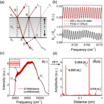
When a semi-transparent sample is placed in beam of coherent monochromatic electromagnetic radiation, and absorption is small, Fabry-Pérot interference can be observed in both the reflected and transmitted radiation. The interference condition can be easily deduced using Snell’s law and geometryHecht (2002) (See Fig. 1a) to be . Here, is the optical path length difference between rays in Fig. 1a, is the sample thickness, is the incident angle, and and are the wavelength dependent real refractive indices of the sample and the medium surrounding the sample, respectively. Hence, whenever equals an integer multiple of the incident wavelength, the transmitted beam constructively interferes and peaks in intensity, while constructive interference for reflected beams occurs when equals half an odd integer multiple.
When a polychromatic source impinges on a sample, the reflectance and transmittance spectra will show Fabry-Pérot interference as a function of wavelength. These undulations can then be used to deduce the sample’s thickness as follows. Starting with two close wavelengths and , such that the complex refractive index , we can take the difference between each wavelength’s interference conditions and solve for , such that
| (1) |
Here we have expressed wavelengths and in wavenumbers () and is the number of peaks (or troughs) between and . To illustrate the use of this method, the top panel of Fig. 1b shows the reflectance spectrum of a piece of double side polished Si wafer, specified by the manufacturer to be m thick (and cm). With , cm-1, (See Ref. 20 for details of the experimental setup) and Palik (1985), we find m. This is consistent with optical modelling in RefFitKuzmenko, A. B. (2005) (black dashed line in Fig. 1b), using the well documented complex refractive index of SiPalik (1985), which also yields a value of m.
II Fourier Transform Analysis
It is clear that eq. 1 is an effective tool for the thickness determination of crystalline wafers, or samples with minimal thickness inhomogeneity. However, when layered materials are cleaved prior to measurements, smooth surfaces are difficult to prepare. Consequent beating between frequencies originating from sample regions of various thickness rule out the manual application of eq. 1. Moreover, optical modelling of spectra that show beating is extremely challenging, while experimental parameters (e.g. sample alignment, surface roughness, imperfect data normalization/referencing, etc.) further complicate the analysis. For example, the bottom panel of Fig. 1b shows the reflectance of Si divided by its reflectance model. Despite the ostensibly successful fit, an additional long range undulation is observed, with a periodicity of that of the Fabry-Pérot due to Si. This undulation is caused by Fabry-Pérot inside a polypropylene window in our setup (as we show later), which did not divide out perfectly when the reflectance intensity of Si was referenced with gold reflectance.
As a solution to this problem we propose the application of Fourier analysis of optical spectra. A similar approach has previously been used in the context of integrated optics, where Fourier analysis of optical transmission data through a waveguide with a microcavity was used to determine the cavity’s mode numbers.Blom et al. (1997) Starting with any wavenumber dependent spectrum (e.g. Reflectance, Transmittance, or unreferenced Intensity), apodized between wavenumbers and such that all visible Fabry-Pérot interference fringes are included, a Fast Fourier TransformCooley, Lewis, and Welch (1969)
| (2) |
yields a position () dependent complex quantity . Here corresponds to the number of equally spaced data points between and (i.e. the resolution of spectrum ). We note that is the inverse of the average spacing between fringes of one frequency in and thus corresponds to the position of maxima in the amplitude of . Hence, the peak position in corresponds to a sample thickness of
| (3) |
To illustrate this approach, we turn to Si once more. Fig. 1c shows the Intensity spectrum (i.e. unreferenced reflectance) of the same m thick Si wafer described before. The amplitude of the Fourier transformed is shown in Fig. 1d, revealing 3 distinct peak positions. Starting with cm, and Palik (1985), we find m, in excellent agreement with our previous results. The third peak at cm is a harmonic of (i.e. interference from higher order internal reflections such as in Fig. 1 a). Finally, the cm peak originates from a 75 m thick polypropylene window used in the experimental setup. With ,Pol (2010); Birch (1992) we find m, in good agreement with the manufacturer’s specifications. We note that Fabry-Pérot interference from windows can, in principle, be removed by a reference measurement. However, nonlinear detectors, optical misalignment, and various other effects can result in residual Fabry-Pérot undulations even in corrected spectra. Hence, to illustrate how our technique can also register and correct such effects, we analyzed the unreferenced reflectance spectrum of Si.
Besides resolving the sample thickness (or if is already known), a major utility of the Fourier analysis approach is that the peaks in , associated with the sample thickness, can be easily removed, even without knowing or . A subsequent inverse Fourier transform then yields the original optical spectrum, devoid of Fabry-Pérot interference, as shown by the black line in Fig. 1c. This can greatly enhance the quality of optical fits, and reveals spectral features previously obscured by strong undulations. Moreover, even systemic sources of Fabry-Pérot fringes, such as windows, polarizers, or other optical elements, can be easily identified and removed, as illustrated in the Si example.
III Results and discussion
Before applying this technique to cleaved van der Waals bound materials, it is useful to discuss what can be expected. One of the underlying assumptions of the described approach is that absorption is minimal and is constant over the chosen spectral range. Since , where is the complex dielectric function, we have . Hence, as long as (i.e. minimal absorption) and constant (i.e. is constant), the Fourier transform approach works very well. However, while this approximation generally gains validity as , the smallest resolvable spectral feature of the Fourier transform is inversely proportional to .Davis, Abrams, and Brault (2001) A balance must thus be sought where a sufficiently large spectral range is chosen that includes all spacial frequencies associated with expected sample thicknesses. Hence, the inevitable finite dispersion of across the selected spectral range will cause the peaks in to broaden.
We note that peak broadening also occurs for samples with a smooth thickness gradient. Indeed, this is commonly exploited in optical measurements, where deliberately wedged samples are used to suppress Fabry-Pérot fringes. In mechanically cleaved samples, however, such a smooth gradient is unlikely.
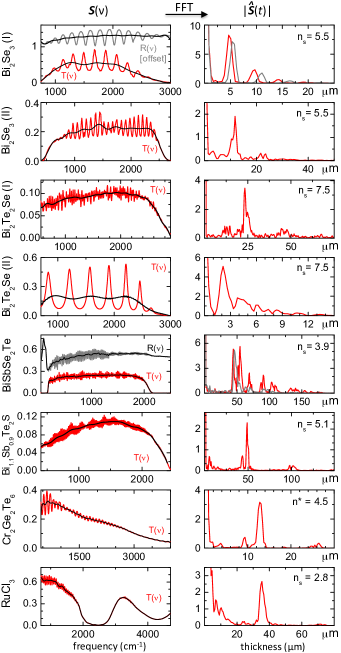
Fig. 2 shows the optical spectra (left panel) of six different materials, where separate measurements on samples with identical stoichiometry are designated by a I or II. With the exception of both Bi2Se3 samples and the Bi2Te2Se (II) sample, all spectra were recorded at the University of Toronto using a modified Bruker Vertex 80v FTIR interferometer, described elsewhere.Reijnders et al. (2014) Spectra of Bi2Se3 and Bi2Te2Se (II) were digitized from previous publications.LaForge et al. (2010); Segura et al. (2012); Akrap et al. (2012) All Bi-containing samples and Cr2Ge2Te6 were grown at Princeton University,Xiong et al. (2012b); Ji et al. (2013) and RuCl3 was grown in Toronto.Plumb et al. (2014) Prior to reflectance or transmittance measurements, samples were mechanically cleaved using tape or were measured as-grown (RuCl3), with typical thickness m. The right panel shows the Fourier transform of the optical spectra. Since it is easier to work with a thickness distribution rather than an optical thickness distribution , we used eq. 3 to plot all spectra with thickness in microns on the -axis. To do so, we assumed that and for the digitized Bi2Se3 and Bi2Te2Se (II) spectra, and estimated (the measured value at 8000 cm-1) for Cr2Ge2Te6. Real refractive index values for all other samples were measured in Toronto,Reijnders and Burch (2014); Reijnders et al. (2014); Sandilands et al. (2014) or reported in the literature.Kohler and Becker (1974)
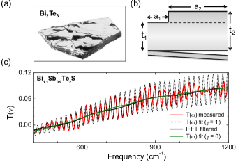
Most notably, all plots show a single dominant peak accompanied by various smaller peaks, where the dominant peak is associated with the most prominent sample thickness. To further confirm this interpretation, the thickness of both BiSbSe2Te and Bi1.1Sb0.9Te2S crystals were independently determined with a (mechanical) digital thickness gauge, and found to be m for both samples (as predicted by our Fourier analysis shown in Fig.2). The smaller peaks in either result from discrete sample thickness variations (e.g. 14 m for Cr2Ge2Te6), or are due to harmonics as observed in Si (e.g. 100 m = m for Bi1.1Sb0.9Te2S, or 9 m = m, and 13.5 m = m for Bi2Se3 (I)). Such discrete sample thickness variations (i.e. inhomogeneity in the -plane) can be easily understood by inspecting the surface of (poorly) cleaved layered materials, such as Bi2Te3 shown in Fig. 3a. These samples can be modelled as an effective medium, where the total measured optical response is a sum of volume fractions multiplied by their respective optical response function. For example, the measured reflectance of a sample with two regions of different thickness (as shown in the top half of Fig. 3 b) would be . Here, and are a function of volume fractions and , respectively, and are the squared magnitudes of the associated complex Fresnel reflection coefficients.
We note that inhomogeneity in the -direction, such as voids inside a crystal (as shown in the bottom half of Fig. 3 b) could also produce multiple peaks in . However, in such a scenario the total optical response would be given by the squared norm of the sum of Fresnel coefficients (e.g. where are reflection coefficients for each interface in the multilayered sample). In other words, for inhomogeneity along , the complex amplitudes are added, as opposed to intensities for inhomogeneities. Therefore, cross terms in result in sums and differences of the various Fabry-Pérot frequencies. Although we see no obvious signatures of this effect in Fig. 2, it can be used as a discriminating technique in determining sample integrity. We note that detection of such additional thin layers may be difficult since the typical resolution of is m. Hence, it is possible that the observed width of the peaks in , even when constant, is a result of unresolved peaks from inhomogeneities in the direction, symmetrically positioned below and above the dominant peak. Regardless, from the many peaks in (and Fig. 3a) it is clear that none of the layered materials produce an optically flat surface across the full sample when cleaved. The observation of Fabry-Pérot fringes, however, does imply high surface quality for all individual regions of constant thickness.
In principle, all peaks can be fitted so that their center position, width and spectral weight can be used to replicate the measured Fabry-Pérot fringes in an optical model. More convenient, however, is to remove the appropriate peaks from , and fit its inverse Fourier transform spectrum with a model that ignores Fabry-Pérot. The black lines in the left panels of Fig. 2 show the result of such optical spectra, in which all Fabry-Pérot fringes have been removed. To confirm that such filtering only removes the Fabry-Pérot fringes, and preserves all other spectral information, the transmittance of Bi1.1Sb0.9Te2S was fit with a model that captures the Fabry-Pérot fringes reasonably well, as shown in Fig. 3b. With the degree of coherence () being a variable in our model, the Fabry-Pérot fringes were artificially suppressed (), as shown by the green line in Fig. 3b. It is clear that the FFT filtered spectrum (black line) matches the optical model with very well, thus confirming that all spectral information but the Fabry-Pérot fringes are preserved.
A comparison of Bi1.1Sb0.9Te2S ( m), Bi2Te2Se I ( m), Bi2Se3 II ( m), and Bi2Te2Se II ( m), shows that as samples get thinner, it becomes increasingly difficult to distinguish thickness related Fabry-Pérot from features due to intrinsic electronic structure. This is particularly clear for RuCl3, where samples with m would produce Fabry-Pérot fringes that are hard to distinguish from intrinsic electronic absorption. Nevertheless, a major advantage of this Fourier transform filter technique is that it addresses only specific frequencies associated with Fabry-Pérot interference, while no knowledge of the refractive index is required.
Finally, we discuss the comparison of reflectance and transmittance spectra on the same sample, as measured for Bi2Se3 (I) and BiSbSe2Te. The interference condition described in section I predicts that for identical values for and , the Fabry-Pérot fringes of reflectance and transmittance spectra should overlap, so that . However, from Fig. 2 it is clear that this is not always the case. While we cannot comment on the experimental conditions under which the Bi2Se3 (I) spectra were obtained,Segura et al. (2012) it is possible that the sample was cleaved between and measurements (thus reducing the thickness), or the incident angle changed between measurements. For BiSbSe2Te, we note that the unique setup in TorontoReijnders et al. (2014) allows and to be identical for both and measurements on a single sample (i.e. thickness remains constant too). The presence of additional peaks in the spectra, not visible in could indicate the presence of (partially) detached flakes on the back surface of the sample, to which only transmission measurements are sensitive. Such a scenario is illustrated in Fig. 3b, and occasionally observed upon careful visual inspection of the sample’s surface when the flake is sufficiently detached from the bulk crystal. While this can only be confirmed with alternative techniques (e.g. x-ray diffraction or Scanning Electron Microscopy), it would be of considerable relevance. In topological insulators, such as BiSbSe2Te, multiple surfaces would result in a greater surface state contribution to optical/electronic properties; a scenario that has been previously suggested.Akrap et al. (2012); Jenkins et al. (2010); Cao et al. (2012) An alternative explanation for the mismatch between and , however, is the imperfect overlap of the probed sample regions between and , as a result of misalignment, beam clipping, or chromatic aberrations.
IV Conclusion
In this letter, we have shown how Fourier analysis of optical spectra offers some previously unexplored opportunities in the study of novel materials. When the real refractive index of a material is known, this technique provides a quick measure of the sample thickness and discrete thickness variations of semi-transparent samples, without the application of a physical (potentially destructive) probe. Moreover, even without knowledge of the refractive index, the inverse Fourier transform of a filtered thickness spectrum yields an optical spectrum devoid of Fabry-Pérot fringes. Such treatment can expose previously obscured features, and can also be used to remove the strong optical effects of sample substrates, windows, or other optical components that cause Fabry-Pérot interference.
We have shown how this technique is applicable not only to carefully manufactured semiconductors, such as Si wafers, but also to a wide variety of cleavable materials, including topological insulators, thermoelectrics, and magnetic insulators. Hence, with recent renewed interest in novel layered samples, we believe this technique makes a valuable addition to standard optical analysis techniques.
Acknowledgements.
This work has been partially funded by the Ontario Research Fund, the Natural Sciences and Engineering Research council of Canada, and the Canada Foundation for Innovation. The crystal growth work at Princeton university was supported by the NSF MRSEC grant DMR 0819860 (topological insulators) and AFOSR MURI grant FA9550-10-1-0553 (thermoelectrics).References
- Novoselov et al. (2004) K. S. Novoselov, A. K. Geim, S. V. Morozov, D. Jiang, Y. Zhang, S. V. Dubonos, I. V. Grigorieva, and A. A. Firsov, Science 306, 666 (2004).
- Xu et al. (2013) M. Xu, T. Liang, M. Shi, and H. Chen, Chemical Reviews 113, 3766 (2013).
- Geim and Grigorieva (2013) A. K. Geim and I. V. Grigorieva, Nature 499, 419 (2013).
- Reina et al. (2009) A. Reina, X. Jia, J. Ho, D. Nezich, H. Son, V. Bulovic, M. S. Dresselhaus, and J. Kong, Nano Letters 9, 30 (2009).
- Park (2011) J.-U. Park, Nature Materials 11, 120 (2011).
- van der Zande (2013) A. M. van der Zande, Nature Materials 12, 554 (2013).
- Butler et al. (2013) S. Z. Butler, S. M. Hollen, L. Cao, Y. Cui, J. A. Gupta, H. R. Gutiérrez, T. F. Heinz, S. S. Hong, J. Huang, A. F. Ismach, E. Johnston-Halperin, M. Kuno, V. V. Plashnitsa, R. D. Robinson, R. S. Ruoff, S. Salahuddin, J. Shan, L. Shi, M. G. Spencer, M. Terrones, W. Windl, and J. E. Goldberger, ACS Nano 7, 2898 (2013).
- Wang et al. (2012) H. Wang, L. Yu, Y.-H. Lee, W. Fang, A. Hsu, P. Herring, M. Chin, M. Dubey, L.-J. Li, and J. Kong, IEEE , IEDM12 (2012).
- Kim et al. (2008) K. S. Kim, Y. Zhao, H. Jang, S. Y. Lee, J. M. Kim, K. S. Kim, J.-H. Ahn, P. Kim, J.-Y. Choi, and B. H. Hong, Nature 457, 706 (2008).
- Bonaccorso et al. (2013) F. Bonaccorso, A. Lombardo, T. Hasan, Z. Sun, L. Colombo, and A. C. Ferrari, Materials Today 15, 564 (2013).
- Zhao et al. (2011) S. Y. F. Zhao, C. Beekman, L. J. Sandilands, J. E. J. Bashucky, D. Kwok, N. Lee, A. D. LaForge, S. W. Cheong, and K. S. Burch, Applied Physics Letters 98, 141911 (2011).
- Sandilands et al. (2010) L. Sandilands, J. Shen, G. Chugunov, S. Zhao, S. Ono, Y. Ando, and K. Burch, Physical Review B 82, 064503 (2010).
- LaForge et al. (2010) A. D. LaForge, A. Frenzel, B. C. Pursley, T. Lin, X. Liu, J. Shi, and D. N. Basov, Physical Review B 81, 125120 (2010).
- Tran et al. (2014) M. K. Tran, J. Levallois, P. Lerch, J. Teyssier, A. B. Kuzmenko, G. Autès, O. V. Yazyev, A. Ubaldini, E. Giannini, D. van der Marel, and A. Akrap, Physical Review Letters 112, 047402 (2014).
- Xiong et al. (2012a) J. Xiong, A. C. Petersen, D. Qu, Y. S. Hor, R. J. Cava, and N. P. Ong, Physica E: Low-dimensional Systems and Nanostructures 44, 917 (2012a).
- Forro et al. (1990) L. Forro, G. L. Carr, G. P. Williams, D. Mandrus, and L. Mihaly, Physical Review Letters 65, 1941 (1990).
- Frindt (1965) R. F. Frindt, Physical Review 140, A536 (1965).
- Frindt (1972) R. F. Frindt, Physical Review Letters 28, 299 (1972).
- Hecht (2002) E. Hecht, Optics, 4th ed. (Addison Wesley, 2002).
- Reijnders et al. (2014) A. Reijnders, Y. Tian, L. J. Sandilands, G. Pohl, I. D. Kivlichan, S. Y. Frank Zhao, S. Jia, M. E. Charles, R. J. Cava, N. Alidoust, S. Xu, M. Neupane, M. Z. Hasan, X. Wang, S. W. Cheong, and K. S. Burch, Physical Review B 89, 075138 (2014).
- Palik (1985) E. D. Palik, Handbook of Optical Constants of Solids, (Academic Press, Boston, 1985).
- Kuzmenko, A. B. (2005) Kuzmenko, A. B., Rev. Sci. Instrum. 76, 083108 (2005).
- Blom et al. (1997) F. C. Blom, D. R. van Dijk, H. J. W. M. Hoekstra, A. Driessen, and T. J. A. Popma, Applied Physics Letters 71, 747 (1997).
- Cooley, Lewis, and Welch (1969) J. W. Cooley, P. A. W. Lewis, and P. D. Welch, IEEE Transactions on Education 12, 27 (1969).
- Pol (2010) Refractive index for Polypropylene from manufacturers specifications (2010).
- Birch (1992) J. R. Birch, Infrared physics 33, 33 (1992).
- Davis, Abrams, and Brault (2001) S. Davis, M. Abrams, and J. Brault, Fourier Transform Spectrometry (Elsevier Science, 2001).
- Segura et al. (2012) A. Segura, V. Panchal, J. F. Sánchez-Royo, V. Marín-Borrás, V. Munoz-Sanjosé, P. Rodríguez-Hernández, A. Munoz, E. Pérez-González, F. J. Manjón, and J. González, Physical Review B 85, 195139 (2012).
- Akrap et al. (2012) A. Akrap, M. Tran, A. Ubaldini, J. Teyssier, E. Giannini, D. van der Marel, P. Lerch, and C. C. Homes, Physical Review B 86, 235207 (2012).
- Xiong et al. (2012b) J. Xiong, Y. Luo, Y. Khoo, S. Jia, R. J. Cava, and N. P. Ong, Physical Review B 86, 45314 (2012b).
- Ji et al. (2013) H. Ji, R. A. Stokes, L. D. Alegria, E. C. Blomberg, M. A. Tanata, A. Reijnders, L. M. Schoop, L. Tian, R. Prozorov, K. S. Burch, N. P. Ong, J. R. Petta, and R. J. Cava, Journa of Applied Physics 114, 114907 (2013).
- Plumb et al. (2014) K. W. Plumb, J. P. Clancy, L. Sandilands, V. V. Shankar, Y. F. Hu, K. S. Burch, H.-Y. Kee, and Y.-J. Kim, arXiv , 1403.0883v2 (2014).
- Reijnders and Burch (2014) A. Reijnders and K. S. Burch, (To be published) (2014).
- Sandilands et al. (2014) L. J. Sandilands, A. A. Reijnders, K. W. Plumb, Y.-J. Kim, and K. S. Burch, (To be published) (2014).
- Kohler and Becker (1974) H. Kohler and C. Becker, Physica Status Solidi B 61, 533 (1974).
- Jenkins et al. (2010) G. Jenkins, A. Sushkov, D. Schmadel, N. Butch, P. Syers, J. Paglione, and H. Drew, Physical Review B 82, 125120 (2010).
- Cao et al. (2012) H. Cao, J. Tian, I. Miotkowski, T. Shen, J. Hu, S. Qiao, and Y. P. Chen, Physical Review Letters 108, 216803 (2012).