Data transmission in long-range dielectric-loaded surface plasmon polariton waveguides
1 Introduction
Optical components, exploiting properties of surface plasmon polaritons (SPP) as guided waves, unlock one of the ways to on-chip photonics, which demands high data bandwidth, low power consumption, and small footprint of the integrated circuits [1]. SPP represents a surface wave, propagating along a boundary between two media, which possess opposite signs of the real part of permittivity (for instance, metal at the frequencies lower than the plasmonic frequency and dielectric). Electrons on a metal boundary can perform coherent with electromagnetic field collective motion [2], and thus support a strong mode confinement at the subwavelength scale, which is an attractive feature allowing to scale down the size of integrated optical circuitry.
Various of nanoplasmonic devices starting from passive components like waveguides [3, 4], couplers and polarization beam combiners [5, 6], to active components, e.g. ring and disk resonators [7, 8, 9], and modulators [10, 11, 12] have been recently demonstrated. Authors of [3] reported a successful transmission of 480 Gbit/s aggregated data traffic (12 channels 40 Gbit/s) over dielectric loaded plasmonic waveguides.
Dielectric-loaded SPP waveguides (DLSPPWs) consist of a dielectric stripe deposited on top of a metallic film and represent one of the basic configurations of the plasmonic waveguides [13]. DLSPPWs demonstrate sub-wavelength confinement of SPPs with the typical propagation distance of at wavelength [14]. The propagation length can be significantly improved in the so-called long-range DLSPPWs (LR-DLSPPWs) that provide both mm-long SPP guiding and relatively tight mode confinement [15, 16]. Experimental investigations of LR-DLSPPWs operating at continuous-wave telecommunication band signal () demonstrated propagation length with the mode size [17]. In this paper we report successful transmission of 10 Gbit/s on-off-keying (OOK) modulated signal through the LR-DLSPPWs with almost negligible degradation of the data flow consistency.
2 Data transmission experiment
2.1 Description of the tested waveguides
The detailed description of similar waveguides is presented in [17]. The waveguiding structure is fabricated by spin-coating of a 255 nm thick layer of UV-curable organic-inorganic hybrid material (Ormoclear, = 1.53) onto a 4 m thick amorphous fluoropolymer (Cytop, = 1.34) coated SiO2 wafer. On the top of the Ormoclear layer there are gold stripes covered with PMMA ( = 1.49). The purpose of the gold stripe is to provide a strong confinement of the electromagnetic wave. The width of the produced PMMA ridges is close to 1 m, which ensures the single-mode operation. The structure of the waveguide is depicted in Fig. 1.
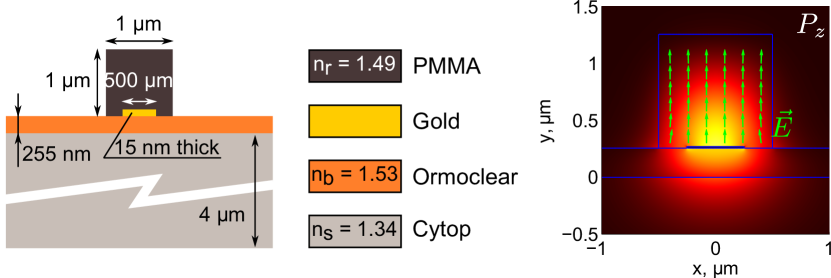
The investigated waveguide has length of 300 m. One side of the optical chip with patterned DLSPPWs was cleaved. The opposite side of the waveguide is terminated by a DLSPP taper with a diffraction grating etched on it. The grating scatters light at angle of 15∘ relative to the vertical direction.
2.2 Prototype of the transmission line
In the performed tests, a typical prototype of a fiber optic telecommunication line, consisting of transmitter (blocks 1–8), receiver (11–19) and device under test (DUT)(9–10), was used (see Fig. 2).
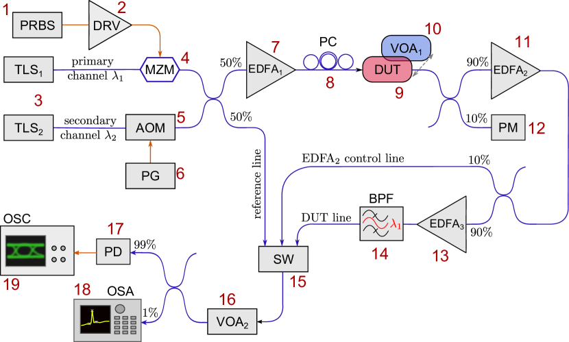
The transmitter unit includes two tunable, independently modulated laser sources (TLS), multiplexed using a 50/50% coupler and pre-amplified using an erbium-doped fiber amplifier (EDFA1). A laser of the primary channel (CH1) is modulated using a Mach-Zehnder modulator (MZM). The MZM is driven with 10 Gbit/s electrical signal that represents a pseudorandom bit sequence (PRBS) with a length of bits. A secondary channel (CH2) laser is modulated with a low-rate 2 Mbit/s square wave signal using an acousto-optical modulator (AOM). The total output power of EDFA1 is kept constantly at the level of 20 dBm to prevent a thermal damage of the waveguides. A polarization controller (PC) is used to ensure the TM polarization of the light, injected into LR-DLSPPW.
After a propagation through the DUT, a weak signal is amplified by means of two cascaded EDFAs (11, 13). An optical band-pass filter (BPF) (0.2 nm FWHM) is used to demultiplex the CH1 signal. Then, a variable optical attenuator (VOA2) reduces the signal down to the level not exceeding a saturation limit of the photodetector (PD) (6 dBm), and the signal is split between the PD (99%) and an optical spectrum analyser (OSA). The electrical signal from PD is transferred to a sampling oscilloscope (OSC).
2.3 Light in- and out-coupling
The DUT includes, besides the test waveguide, a corresponding light coupling system (Fig. 3). An input signal is coupled into the facet of waveguide using a tapered and lensed optical fiber. The output signal is collected with a cleaved optical fiber placed in the vicinity of the grating, which terminates the waveguide.
Piezo-driven stages 7–9 are used for a precise alignment of optical fibers and the sample. The lensed fiber for in-coupling is held in a V-groove 6 and clamped with rare-earth magnets. The collecting cleaved fiber is glued into a ceramic ferrule, which is fastened up in a holder on a rotating platform. Such configuration allows us to place the fiber facet near the scattering grating and vary the collecting angle, which should be about 15∘.
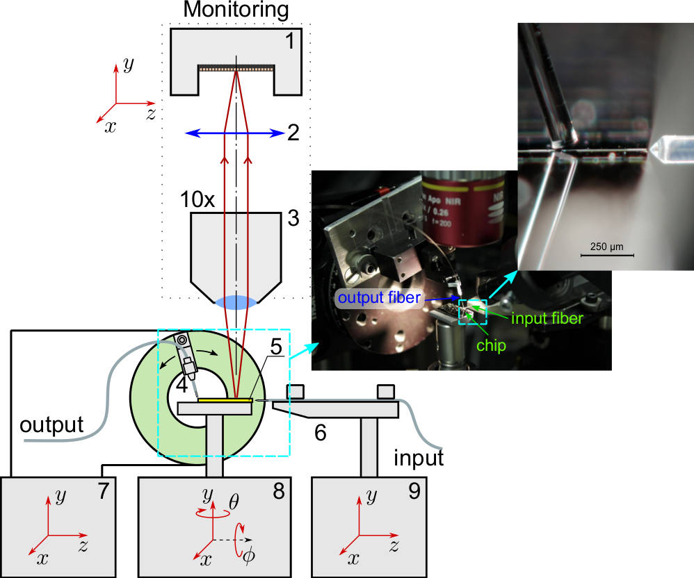
The sample is illuminated by a pair of incandescent fiber optic illuminators and is observed with two digital cameras. An infrared camera from company Xenics 1 is attached on top of a microscope, which consists of a 10 Mitutoyo IR objective 3 (working distance of 32 mm) and a 200 mm achromat tube lens 2.
Another monitoring tool is the Canon EOS 60D single-lens reflex photocamera mounted with the Canon EF MP-E 65 mm macrolens that provides 5 magnification. The photocamera is used to observe the sample from a side (see Fig. 3, inset). It is placed on a motorized linear translation rail (StackShot from Cognisys Inc.), which allows precise focusing. The purpose of the photocamera is to estimate the elevation of optical fibers above the surface of the sample.
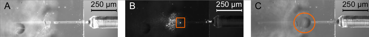
The fiber alignment procedure starts from the positioning of two light sources in a such way, that both the waveguides and the gratings are clearly visible (see Fig. 4A). Light, which is irradiated in the transversal direction, gets reflected from the edges of the waveguides, whereas light going longitudinally scatters from the gratings.
After the waveguides are clearly seen, the tapered fiber is positioned in the vicinity of the waveguide facet (see Fig. 4A). Next, the intensity of the illumination is reduced and a weak IR signal is sent through the tapered fiber. The latter one is aligned until one can see a strong emission from the grating (illustrated in Fig. 4B).
Then the cleaved fiber is brought into the vicinity of the grating (see Fig. 4C) and is moved down under the monitoring from the VIS camera. The intensity of the IR signal is increased up to 20 dBm, and coupling is optimized to achieve a maximal output signal.
2.4 Evaluation of bit error rate
The bit error rate (BER) is evaluated from eye diagrams, captured by a sampling oscilloscope. The device acquires a considerable amount of waveforms and uses them to calculate a histogram of a signal voltage. This histogram represents the statistics of data hits in the specified window, anchored to the center of the eye (see Fig. 5). For the sufficiently large number of hits in the histogram window ( hits), the normalized histogram approximates the probability distribution function (PDF) of the received electrical signal – logic ones and zeros.
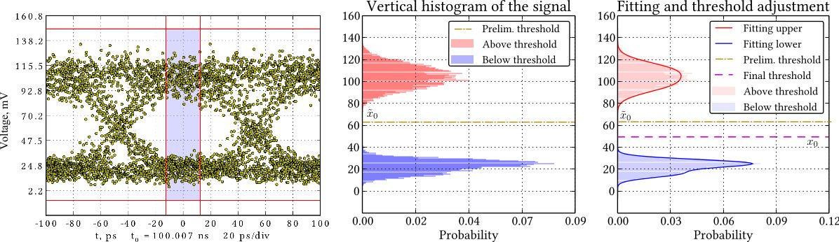
The histogram must be normalized before one can extract any statistics from it. If the histogram is represented as , where is the number of hits in a small interval and is the instantaneous voltage, then the normalized histogram is found as:
| (1) |
This results in a unit area under the histogram given by formula.
The averaged voltage value is used as a preliminary decision threshold :
| (2) |
It is used to split the histogram into upper (corresponding to the binary one) and lower (binary zero) parts.
The PDFs of one and zero are close to Gaussian ones, but under the certain conditions a pair of close peaks is observed in each semi-histogram. Therefore, we perform fitting of the semi-histogram with a sum of two Gaussians (see Eq. 3). The selection of an appropriate starting estimation plays a crucial role for a good fitting. For this reason we specify fitting functions and based on the statistics extracted from semi-histograms. The fitting function for logical one is:
| (3) |
where is the mean value and is the standard deviation of data in the upper semi-histogram, which is supposed to be close to the normal distribution function.
| (4) | ||||
| (5) |
The analogous relations are valid for the function.
The fitting functions and intersect with each other at the decision threshold value . Therefore, the is found as a numerical solution of equation:
| (6) |
BER value is defined by a numerical integration of the overlapped regions according to formula:
| (7) |
2.5 Estimation of BER penalties
Each experiment is performed as following:
-
1.
LR-DLSPPW is placed into the coupling setup (together they form DUT, item 9 in Fig. 2), and the BER at different values of received optical power (ROP) is determined.
-
2.
The DUT is replaced by the optical attenuator (VOA1, item 10 in Fig. 2), which provides the same value of insertion losses as DUT does (typically of about –42 dB), and a set of reference back-to-back measurements (B2B) is carried-out. During the B2B test the BER vs. ROP values are determined in the same way as described above.
-
3.
Q-factor of the signal is retrieved from BER, according to the inverse function , where is calculated from [18]:
(8) -
4.
The fitting of Q-factor vs. ROP is performed using the equation:
(9) -
5.
The BER dependency is evaluated using Eq. 9 both for DUT and B2B tests.
-
6.
BER penalties, which characterize the data signal degradation in the presence of DUT, are defined as:
(10)
3 Results
The performed experiments on data transmission can be divided into subgroups, which differ by:
-
1.
Number of transmitted channels;
-
2.
Channel wavelengths;
-
3.
Spacing between channels.
The number of channels is limited by the total gain of post-amplifiers (items 11 and 13 in Fig. 2). As the total power of the injected signal should be kept constant, adding extra channels to the system involves dB reduction of the power level of every channel. Thus, the gain of the post-amplifies should be increased by the same amount to maintain the channel power constant. From the other side, an input power to the waveguide is increased with the number of channels, which finally can lead to the thermal damage to the waveguide.
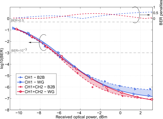
As it was described in the previous section, one or two channel signals have been transmitted through the LR-DLSPPW. Results of experiments with single and double channel (0.4 nm spacing) data transmission at 1549 nm are presented in Fig. 6. It should be noted that the BER penalties remain below 0.5 dB in the ROP range of interest from to dBm (lower detected powers results in the BER that exceeds threshold required for the proper operation of forward error correcting codes (FEC) [19, 20, 21]). Moreover, we managed to achieve BER as low as .
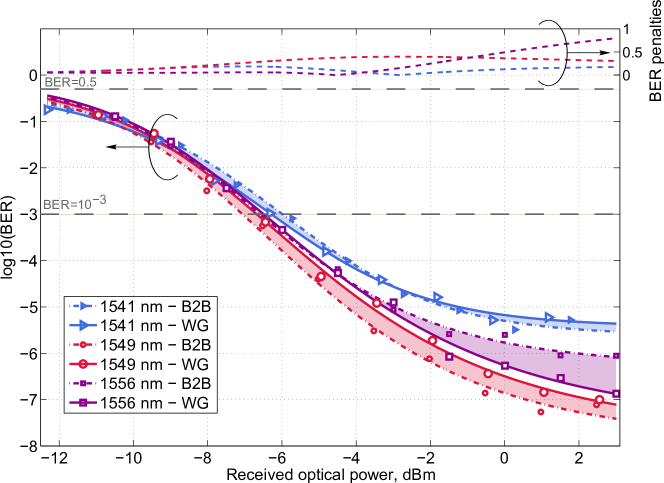
The BER dependence on the transmitted wavelength has been studied in three different wavelength regions (Fig. 7). As in the previous case, BER penalties do not exceed 0.6 dB at ROP from to dBm. The full wavelength region under study was limited by the gain profile of exploited EDFAs. In some cases back-to-back measurements turned out to be a bit worse than the respective ones with the waveguide. We intend to attribute these discrepancies to the adopted in this paper method of the BER evaluation.
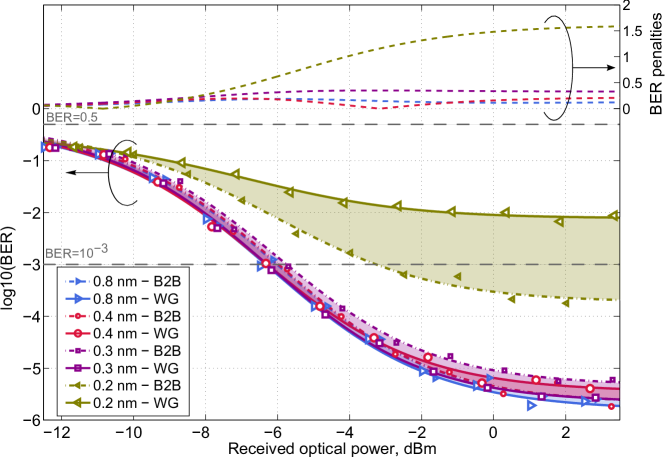
Finally, we evaluated BER penalties originating from the signal crosstalk by changing the spectral distance between channels (Fig. 8). BER penalties below 0.5 dB are obtained for the wavelength spacing as low as 0.3 nm (). However, penalties of nearly 1.5 dB are estimated for the channel spacing of 0.2 nm (), indicating the presence of channel crosstalk in the LR-DLSPPW. The appeared cross talk at the channel separtion of 2 nm is caused by a band pass filter that was placed before the receiver. The purpose of the filter is to select a single channel; however, the filter bandwidth is about 0.2 nm, which is comparable with the channel separation, so the receiver additionally detects signal from the wrong channel.
4 Summary
In conclusion, we have demonstrated the data transmission of 10 Gbit/s on-off keying modulated 1550 nm light wave through a LR-DLSPPW structure with negligible signal degradation. The BER penalties do not exceed 0.6 dB over the 15 nm wavelength range and ROP between and dBm. The BER penalties were determined by the comparison of LR-DLSPPW structure with an optical attenuator that provides the same insertion loss. We should note, however, that the main contributor to the observed insertion loss is the light scattering at the interfaces between waveguide facets and the optical fibers of the testbench.
The achieved results show the applicability of LR-DLSPP waveguiding structures for the data transmission in integrated photonic interconnects. It demonstrates long propagation distances together with the subwavelength mode confinement; recent studies [17] show that the waveguide could be patterned along curved lines or even be split in two. Moreover, authors of [22] present techniques for loss compensation in LR-DLSPPW modes by means of stimulated emission. Such unique combination of features holds promise for implementation of compact and powerful integrated plasmonic circuits for fast photonic data processing devices.
References
- [1] Volker J. Sorger, Rupert F. Oulton, Ren-Min Ma and Xiang Zhang “Toward integrated plasmonic circuits” In MRS Bulletin 37, 2012, pp. 728–738 DOI: 10.1557/mrs.2012.170
- [2] R. H. Ritchie “Plasma Losses by Fast Electrons in Thin Films” In Phys. Rev. 106 American Physical Society, 1957, pp. 874–881 DOI: 10.1103/PhysRev.106.874
- [3] D. Kalavrouziotis et al. “0.48Tb/s (12x40Gb/s) WDM transmission and high-quality thermo-optic switching in dielectric loaded plasmonics” In Opt. Express 20.7 OSA, 2012, pp. 7655–7662 DOI: 10.1364/OE.20.007655
- [4] Jung Jin Ju et al. “40 Gbit/s light signal transmission in long-range surface plasmon waveguides” In Applied Physics Letters 91.17, 2007, pp. 171117 DOI: 10.1063/1.2803069
- [5] Vladimir A. Zenin et al. “Directional coupling in channel plasmon-polariton waveguides” In Opt. Express 20.6 OSA, 2012, pp. 6124–6134 DOI: 10.1364/OE.20.006124
- [6] Argishti Melikyan et al. “Integrated Wire Grid Polarizer and Plasmonic Polarization Beam Splitter” In Optical Fiber Communication Conference Optical Society of America, 2012, pp. OW1E.3 URL: http://www.opticsinfobase.org/abstract.cfm?URI=OFC-2012-OW1E.3
- [7] Sukanya Randhawa et al. “Experimental demonstration of dielectric-loaded plasmonic waveguide disk resonators at telecom wavelengths” In Applied Physics Letters 98.16 AIP, 2011, pp. 161102 DOI: 10.1063/1.3574606
- [8] Tobias Holmgaard et al. “Dielectric-loaded plasmonic waveguide-ring resonators” In Opt. Express 17.4 OSA, 2009, pp. 2968–2975 DOI: 10.1364/OE.17.002968
- [9] A.V. Krasavin and A.V. Zayats “All-optical active components for dielectric-loaded plasmonic waveguides” Nonlinear Optics in Metamaterials In Optics Communications 283.8, 2010, pp. 1581 –1584 DOI: 10.1016/j.optcom.2009.08.054
- [10] Domenico Pacifici, Henri J. Lezec and Harry A. Atwater “All-optical modulation by plasmonic excitation of CdSe quantum dots” In Nat Photon 1.7, 2007, pp. 402–406 URL: http://dx.doi.org/10.1038/nphoton.2007.95
- [11] Argishti Melikyan et al. “Surface plasmon polariton absorption modulator” In Optics express 19.9, 2011, pp. 8855–69 URL: http://www.ncbi.nlm.nih.gov/pubmed/21643139
- [12] A.V. Krasavin et al. “All-plasmonic modulation via stimulated emission of copropagating surface plasmon polaritons on a substrate with gain” * In Nano letters 11 ACS Publications, 2011, pp. 2231–2235 DOI: 10.1021/nl200255t
- [13] Tobias Holmgaard and Sergey I. Bozhevolnyi “Theoretical analysis of dielectric-loaded surface plasmon-polariton waveguides” In Phys. Rev. B 75 American Physical Society, 2007, pp. 245405 DOI: 10.1103/PhysRevB.75.245405
- [14] Tobias Holmgaard et al. “Bend- and splitting loss of dielectric-loaded surface plasmon-polariton waveguides” In Opt. Express 16.18 OSA, 2008, pp. 13585–13592 DOI: 10.1364/OE.16.013585
- [15] Tobias Holmgaard, Jacek Gosciniak and Sergey I. Bozhevolnyi “Long-range dielectric-loaded surface plasmon-polariton waveguides” * In Opt. Express 18.22 OSA, 2010, pp. 23009–23015 DOI: 10.1364/OE.18.023009
- [16] Jacek Gosciniak, Tobias Holmgaard and Sergey I. Bozhevolnyi “Theoretical Analysis of Long-Range Dielectric-Loaded Surface Plasmon Polariton Waveguides” In J. Lightwave Technol. 29.10 OSA, 2011, pp. 1473–1481 URL: http://jlt.osa.org/abstract.cfm?URI=jlt-29-10-1473
- [17] Valentyn S. Volkov et al. “Long-range dielectric-loaded surface plasmon polariton waveguides operating at telecommunication wavelengths” In Opt. Lett. 36.21 OSA, 2011, pp. 4278–4280 DOI: 10.1364/OL.36.004278
- [18] D. Marcuse “Derivation of analytical expressions for the bit-error probability in lightwave systems with optical amplifiers” In Lightwave Technology, Journal of 8.12, 1990, pp. 1816 –1823 DOI: 10.1109/50.62876
- [19] Y.K. Lize et al. “Optical Error Correction using Passive Optical Logic Gates Demodulators in Differential Demodulation” In Lasers and Electro-Optics, 2007. CLEO 2007. Conference on, 2007, pp. 1–2 DOI: 10.1109/CLEO.2007.4452622
- [20] “Ultrahigh-Speed Optical Transmission Technology (Optical and Fiber Communications Reports)” Springer, 2010 URL: http://amazon.com/o/ASIN/3642062822/
- [21] D. Hood “Gigabit-capable Passive Optical Networks” Wiley, 2012 URL: http://amazon.com/o/ASIN/0470936878/
- [22] Jonathan Grandidier et al. “Gain-Assisted Propagation in a Plasmonic Waveguide at Telecom Wavelength” In Nano Letters 9.8, 2009, pp. 2935–2939 DOI: 10.1021/nl901314u