Current-Driven Domain Wall Depinning and Propagation in Notched Nanowires
Abstract
Adiabatic spin transfer torque induced domain wall (DW) depinning from a notch and DW propagation in a nanowire with a series of notches is investigated. Surprisingly, notches help a current to depin a DW and make a DW easier to propagate along a wire. Following fascinating results on DW dynamics are found. 1) The depinning current density of a DW in a notch is substantially lower than the intrinsic threshold value below which a sustainable DW propagation doesn’t exist in a homogeneous wire. 2) The DW displacement from a notch is insensitive to notch geometry and current density when it is between the depinning and the intrinsic threshold current density. 3) A current density below the intrinsic threshold value can induce a sustainable DW propagation along notched nanowires. These findings not only reveal interesting and complicated interaction between a current and a DW, but also have profound implications in our current understanding of current-driven DW dynamics as well as in the design of spintronic devices.
pacs:
75.78.-n, 75.60.Ch,75.78.Cd, 85.75.-dControlled manipulation of domain walls (DWs) in magnetic nanowires is an important topic in nanomagnetism not only for its fundamental interest, but also for its applications in spintronic devices [1, 2, 3] where pinning, depinning, DW displacement, and DW propagation are crucial. Magnetic fields via energy dissipation [4, 5] and electric current via angular momentum transfer [6, 8, 7] are well-known DW control parameters. Although many efforts have been devoted to it and much progress has been made, our current understanding of the subject is still limited and far from satisfactory, especially for DW dynamics involving notches. The pinning field of a DW in a homogeneous nanowire is zero [4, 5]. To pin a DW in a wire, the wire inhomogeneity is necessary and notches are often used in experiments and simulations [9, 10, 11, 12] for positioning a DW. To move a DW out of a notch, a field larger than a critical value, called depinning field, is needed. The depinning field depends sensitively on notch properties as well as DW types [11, 12, 13]. It is so sensitive that depinning fields have been used to distinguished one type of DW from another in experiments [11].
Things are quite different when a current is used to manipulate DWs, as shown by a mysterious observation [11] that depinning current required to move a DW out of a notch does not depend on DW types, which is in a sharp contrast to its magnetic field counterpart. In principle, a current generates an adiabatic spin transfer torque (STT) [6] and a non-adiabatic STT [8, 14]. The mechanism of the adiabatic torque is well established while the non-adiabatic torque is still in debate [15, 16]. The non-adiabatic STT, even existing, is much smaller than the adiabatic one, and it is neglected in many theoretical treatments and analysis. In the absence of the non-adiabatic STT, a current density below a threshold value can only displace a DW for a finite distance when the current is on and the displacement vanishes when the current is off [17, 18]. The transit displacement, which depends on material properties, is on the order of a few hundreds nanometers for permalloy. Only under a current density above the threshold value, the DW can propagate continuously[8, 14, 19]. This phenomenon is called the intrinsic pinning for the adiabatic STT. How an adiabatic STT interacts with a DW trapped in a notch or how the adiabatic STT drives a DW to propagate along a wire with many notches is obviously important [1, 2], but little known. Naively, one may expect that a DW would be further pinned by a notch. Thus, the nature conjecture is that a current density above the threshold value for the homogeneous wire would be required to move the DW out of the notch. It would also be nature to expect that a larger current density is required to induce a sustainable DW propagation along the wire with many notches. In this letter, we numerically study the issue. Surprisingly and fascinatingly, a current density substantially below the threshold value can move a DW out of a notch. The DW is far from the notch when the current is switched off. In fact, the displacement, inversely proportional to the damping and proportional to DW width, is much larger than both the DW width and the transit displacement of the DW in the corresponding homogeneous wire. If one places a series of notches along the wire, a current density much smaller than the intrinsic threshold value can also sustain a continuous DW propagation.
We consider magnetic wires of 5000 nm long, 4 nm thick, and width varying from 48 nm to 120 nm so that transverse DWs are preferred. A triangular/rectangular notch of width and depth is located on the top edge of the wire as shown in Fig. 1. The , , and axis are respectively along the length, width, and thickness directions with the origin at the wire center. The magnetization dynamics is governed by the generalized Landau-Lifschitz-Gilbert (LLG) equation,
| (1) |
where , , , and denote the unit vector of magnetization, gyromagnetic ratio, the Gilbert damping constant and effective field, respectively. includes exchange field and anisotropy field. The third term on the right hand side is the adiabatic STT, where is proportional to the current density and is along the current direction, where , , and are the current polarization, the Bohr magneton, the electron charge and the saturation magnetization, respectively. In our simulations, electrons flow in the -direction (opposite to illustrated in Fig. 1). Thus in this term becomes . The LLG equation is solved numerically by OOMMF package [20]. To mimic permalloy wires, we use the exchange constant J/m, A/m, zero crystalline anisotropy and the damping constant . The mesh size is 4nm4nm4nm.
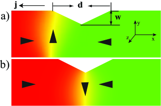
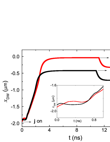
All wires show similar behaviors, and we present the results for a 64 nm wide wire. There are two types of transverse DWs, anticlockwise wall (AW) which prefers to stay near the notch edge as sketched in Fig. 1a and clockwise wall (CW) which tends to reside near the notch center as sketched in Fig. 1b. The intrinsic threshold current density of the corresponding uniform nanowire is m/s only above which a DW can undergo a sustainable propagation. In the presence of a triangular notch of nm and nm centered at nm, a current density of 578 m/s can obviously depin an AW from the notch. The time evolution of the AW position under m/s, on at , is plotted as the red curve in Fig. 2. The AW, pinned at the left edge of the notch initially, moves first in the direction and reaches the right side of the notch in about 0.2 ns. Its center , defined as the average -coordinate of those spins with , does not change much for about 0.4 ns, shown in the enlarged figure in the inset while the DW structure continuously deforms and an antivortex is born at the edge defect of winding number [21] -1/2 on the lower wire edge. Right after the birth of the antivortex, the DW starts to move out of the notch at a constant velocity represented by the linear segment between 0.6 ns and 3.5 ns. The DW stops finally at nm, almost 2 m away from the notch. Intuitively, one will expect that notches tend to strengthen DW pinning so that any current density (measured by ) below would not depin a DW. Thus, what we observed is a very surprising result. When the current is switched off at 11.2 ns, as expected [17], the DW retreats for about 292 nm, the intrinsic transit displacement. At the end of the process, the DW displacement is about 1572 nm which is far away from the notch. This displacement is more than five times of the transit displacement of a DW under the same current density if the wire was uniform. Of course, different from our results, the net DW displacement would be zero n a uniform wire after the current is switched off [17].
The overall CW behavior is very similar to the AW case as shown by the black curve in Fig. 2 for m/s (). The DW center does not change much initially (black line in the inset), probably because the center is already in the right side of the notch, while the DW structure deforms for about 0.6 ns before a vortex appears at the edge defect of winding number 1/2 on the lower wire edge. Similar to the AW case, the DW center starts to move out of the notch, at a constant velocity, after the vortex is born. It stops at nm far out of the notch. When the current is switched off at ns, the DW center retreats for about nm and stops at nm, about 1 m on the right of the notch. There are some subtle differences in comparison with the AW case. An antivortex may also generated at the edge defect of winding number [21]. The final DW displacement depends also on whether an antivortex or a vortex is generated. The details of how many depinning process there are, how a DW is depinned in each process, and what is the phase diagram in the plane will be reported elsewhere.
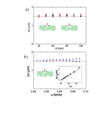
It is interesting to know how the DW displacement depends on (larger than depinning value and smaller than ), the notch type and geometry. Let be the net DW displacement, i.e. the displacement after the current is switched off. Fig. 3a is -dependence of of an AW with rectangular (filled symbols) and triangular (open symbols) notches for m/s (diamonds) and m/s (circles). Surprisingly, does not depend on the notch types and geometry, within numerical accuracy. Fig. 3b is -dependence of for triangular notches of various widths nm (triangles), 64 nm (squares), and 128 nm (circles). depends only weakly on . It is interesting to notice that depinning occurs only when a vortex/antivortex is generated at one of the DW edge defects. DW moves, together with the vortex/antivortex. The DW displacement is the distance that the vortex/antivortex travels in the direction in its lifetime. If this observation is the essential depinning physics, the highly counter-intuitive DW displacement behavior can be understood from the Thiele equation [22, 14, 23] for a vortex. Using the Thiele equation [22, 14, 23], one has
| (2) |
where is the force acted on the vortex core from external field that is zero in our case, is gyrovector, , where is the winding number (+1 for a vortex and -1 for an antivortex) and is the vortex polarity ( for core polarization in direction) and is the thickness of nanowire. is the velocity of the vortex core, where is the core position. is dissipation dyadic, whose none zero elements are [23], where is the Thiele’s DW width [22]. Then the component of the Thiele equation is
The displacement of the vortex core can be obtained by integrating the above equation, and one has
| (3) |
Note that vortex travel distance in direction is . Thus, we show that does not depend on and notch geometry! Eq. (3) (dashed lines without any fitting parameters) explains the numerical results very well as shown in Fig. 3. The dependence is also confirmed numerically as shown in the right inset of Fig. 3b, where crosses denote simulation results and line is Eq. (3). Although not shown explicitly, the displacement of a CW, whose Thiele DW width is smaller than that of a AW, can also be explained by Eq. (3) equally well.
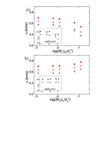
To demonstrate the robustness and generality of the results, we add an extra biaxial crystalline anisotropy of in our simulations, where and are respectively the easy- and hard-axis anisotropy coefficients. Fig. 4 are the () dependence of (filled symbols) and depinning current density (open symbols) for AW (triangles) and CW (squares) when ( ). All other parameters are the same as those for Fig. 2. Fig. 4 shows that the larger the easy-axis (hard-axis) anisotropy is, the smaller (larger) will be, which is consistent with the prediction of a biaxial model [17]. The depinning current density is well below the intrinsic threshold current density as () changes. It is interesting to see that an extra easy-axis anisotropy reduces while hardly affects , as illustrated in the insets of Figs. 4a and 4b, respectively.
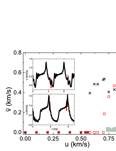
The above results imply that notches should help current-driven DW propagation along a wire instead of hindering the propagation as in the case of field-driven DW motion. To confirm this highly counter-intuitive conjecture, we place a series of triangular notches (of 64 nm wide and 16 nm deep) along the two wire edges alternatively, as illustrated in the low-right inset of Fig. 5. The reason that notches are alternatively placed on the upper and lower edges is because an AW (CW) will change to a CW (AW) after depinning from a notch under the assistance of generated vortices/antivortices on one wire edge that travel to the other edge and die there. Our micromagnetic simulations show that a current density below can induce a sustainable DW propagation when notch separation is chosen properly according to DW displacement from a single notch discussed early. Fig. 5 is the dependence of average DW speed (crosses) when the notch interval is 1800 nm for a wire of 64 nm wide. The average speed is zero for m/s because it is smaller than the depinning value. When the current density increases to m/s, but well below m/s, the DW has a speed of about 500 m/s. The time-dependence of the instantaneous speed at m/s is given in the top-left inset. The DW speed is almost zero at notches (red bars) and is bigger than 500 m/s away from the notches. As the current density increases to , the average speed approaches the DW speed in the corresponding homogeneous wire (red squares). Without a surprise, notches cause the instantaneous DW speed oscillating as shown in the low-left inset at m/s. Interestingly, the instantaneous DW speed at notches (red bars) is near the maximal in contrast to near zero speed for .
The findings presented here should have profound implications on STT-based DW applications as well as our understanding of STT-driven DW dynamics. For example, the original argument for the inclusion of the non-adiabatic STT was based on the experimental observation of DW propagation below the intrinsic threshold current density. The argument relies on an implicit assumption that any wire inhomogeneity shall always increase the depinning current density. Thus, the experimentally observed DW propagation below the intrinsic threshold current density could only be explained by including the non-adiabatic torque. Our findings obviously shake that reasoning. One needs to reexamine the analysis of necessity of the non-adiabatic STT, especially its magnitude.
The contrasting differences between current and field driven DW depinning and DW propagation in notched wires come from different control mechanisms. On the one hand, a magnetic field creates energy density difference between two domains that are separated by a DW. According to Ref. 5, a static DW cannot exist between such two domains if the wire has the translational symmetry. This is why a DW cannot resist to an arbitrary small field. To prevent a DW motion under a field, the translational symmetry has to be destroyed. This could be done by inevitable wire roughness or by intentionally designed notches. On the other hand, a current exerts a torque on a DW through angular momentum transfer. As a result, a DW can deform its structure to absorb the current-generated STT, resulting in the intrinsic threshold current density in a homogeneous wire [17]. The introduction of a notch may weaken the delicate balance between DW structure deformation and adiabatic STT. This may be the origin of our counter-intuitive results. It should be interesting to explore this idea.
In conclusion, we have investigated the adiabatic STT-driven DW depinning and DW propagation in a notched nanowire. Below the intrinsic threshold current density, a DW can be depinned from a notch and be displaced by a long distance that is inversely proportional to the damping constant. In a realistic material, the displacement can be of the order of m. Furthermore, the DW displacement does not depend on the notch type and geometry. It depends also very weakly on the current density as long as the current density is between the depinning and the intrinsic threshold current density. This surprisin result can be explained well by the Thiele equation for vortex dynamics. These findings should have profound implications in both STT-driven DW motion and STT-based DW devices.
This work was supported by the NSF of China grant (11374249) and Hong Kong RGC grant (605413). HYY acknowledges the support of Hong Kong PhD Fellowship.
References
- [1] S. S. P. Parkin, M. Hayashi, and L. Thomas, Science 320, 190 (2008).
- [2] D. A. Allwood, G. Xiong, C. C. Faulkner, D. Atkinson, D. Petit, and R. P. Cowburn, Science 309, 1688 (2005).
- [3] C. Chappert, A. Fert, and F. N. V. Dau, Nat. Mater. 6, 813 (2007).
- [4] N. L. Schryer and L. R. Walker, J. Appl. Phys. 45, 5406 (1974).
- [5] X.R. Wang, P. Yan, J. Lu and C. He, Ann. Phys. (N.Y.) 324, 1815 (2009); X.R. Wang, P. Yan, and J. Lu, Europhys. Lett. 86, 67001 (2009).
- [6] L. Berger, Phys. Rev. B 54, 9353 (1996);J. Slonczewski, J. Magn. Magn. Mater. 159, L1 (1996).
- [7] A. Yamaguchi, T. Ono, S. Nasu, K. Miyake, K. Mibu and T. Shinjo, Phys. Rev. Lett. 92, 077205 (2004).
- [8] S. Zhang and Z. Li, Phys. Rev. Lett. 93, 127204 (2004).
- [9] R. D. McMichael, J. Eicke, M. J. Donahue and D. G. Porter, J. Appl. Phys. 87, 7058 (2000).
- [10] M. Kläui, C. A. F. Vaz, J. Rothman, J. A. C. Bland, W. Wernsdorfer, G. Faini, and E. Cambril, Phys. Rev. Lett. 90, 097202(2003).
- [11] M. Hayashi, L. Thomas, C. Rettner, R. Moriya, X. Jiang, and S. S. P. Parkin, Phys. Rev. Lett. 97, 207205 (2006).
- [12] L. K. Bogart, D. Atkinson, K. O’Shea, D. McGrouther, and S. McVitie, Phys. Rev. B 79, 054414 (2009).
- [13] H. Y. Yuan and X. R. Wang, Phys. Rev. B 89, 054423 (2014).
- [14] A. Thiaville, Y. Nakatani, J. Miltat, Y. Suzuki, Europhys. Lett. 69, 990 (2005).
- [15] S. -M. Seo, K. J. Lee, W. Kim, and T. -D. Lee, Appl. Phys. Lett. 90, 252508 (2007).
- [16] T. Koyama, D. Chiba, K. Ueda, K. Kondou, H. Tanigawa, S. Fukami, T. Suzuki, N.Ohshima, N. Ishiwata, Y. Nakatani, K. Kobayashi, and T. Ono, Nat. Mater. 10, 194 (2011).
- [17] Z. Li and S. Zhang, Phys. Rev. B, 70, 024417 (2004).
- [18] G. Tatara and H. Kohno, Phys. Rev. Lett. 92, 086601 (2004).
- [19] M. Hayashi, L. Thomas, C. Rettner, R. Moriya and S. S. P. Parkin, Nat. Phys. 3, 21 (2007).
- [20] http://math.nist.gov/oommf
- [21] H. Y. Yuan and X. R. Wang, J. Magn. Magn. Mater. 368, 70 (2014).
- [22] A. A. Thiele, Phys. Rev. Lett. 30, 230 (1973).
- [23] D. L. Huber, Phys. Rev. B 26, 3758 (1982).