Development of a highly pixelated direct charge sensor, Topmetal-I, for ionizing radiation imaging
Abstract
Using industrial standard CMOS Integrated Circuit process, we realized a highly pixelated sensor that directly collects charge via metal nodes placed on the top of each pixel and forms two dimensional images of charge cloud distribution. The first version, Topmetal-I, features a pixel array of pitch size. Direct charge calibration reveals an average capacitance of per pixel. The charge collection noise is near the thermal noise limit. With the readout, individual pixel channels exhibit a most probable equivalent noise charge of .
keywords:
Topmetal , pixel , charge sensor1 Introduction
Charge sensors are at the heart of many ionizing radiation detectors. Modern imaging systems often require a simultaneous determination of the amount, position and time structure of charges from ionization. In these cases, a charge sensor of sub-millimeter spatial resolution is highly desirable.
Solid state detector systems, mainly segmented silicon and germanium crystals coupled to CMOS pixel sensors, are widely deployed. CMOS pixel sensors such as Medipix/Timepix[1, 2] and FE-I3/FE-I4 [3] are readily available. They have pixel sizes of tens to hundreds of microns. They are coupled to the crystals through processes such as the flip-chip bump bonding.
On the other hand, for gaseous and liquid detectors, wire and Printed Circuit Board (PCB) are still the most popular readout schemes. Those detectors are often configured as Time Projection Chambers (TPCs [4]). Noticeable imaging systems of such kind are LXeGRIT[5] and -PIC[6]. For practical reasons, it is difficult to realize a multi-wire readout with a wire pitch smaller than a millimeter. Novel designs using PCB have reached a pitch of hundreds of [6]. However, such designs still face challenges of signal readout multiplexing and speed.
Gaseous and liquid detectors have distinct advantages over solid state detectors: they are more easily scalable to large mass and are resilient to radiation damage. Only with an equally scalable yet high resolution charge readout scheme, their superior properties can be exploited in imaging applications. The CMOS pixel sensor is an excellent candidate for this task, because of the fine pixel size, as well as the possibility of embedding complex circuitry for signal paths.
There have been attempts towards the use of CMOS pixel sensors in a TPC to read the charge signal, with limited success. The D3 experiment [7] uses FE-I3/FE-I4 sensors developed for the ATLAS [8] experiment, behind a gaseous electron multiplication stage, to detect charge tracks resulting from potential dark matter interactions. A similar attempt was made to use the Timepix sensor as the readout for a TPC [9].
The development of CMOS sensors is usually dictated by the requirements of large experiments or the consensus of consortiums. Existing sensors either have some high level processing already built-in to handle the massive data rate common in collider experiments, or are lack of low noise analog channels. The readout for gaseous and liquid detectors are often slower, but have more stringent requirement on noise performance.
We set out to realize a CMOS sensor that is uniquely suitable for charge readout in gaseous and liquid detectors. We implemented a direct charge sensor with pitch between pixels using the industrial standard CMOS process. Its behavior in charging collection is well characterized.
2 Sensor Structure and Operation
A photograph of one fully fabricated and wire-bonded Topmetal-I sensor is shown in Fig. 1. The sensor is implemented in a silicon real-estate area. With pitch distance between pixels, the square pixel array makes up a charge sensitive region. Readout interface logic and analog buffers are placed around the pixel array.
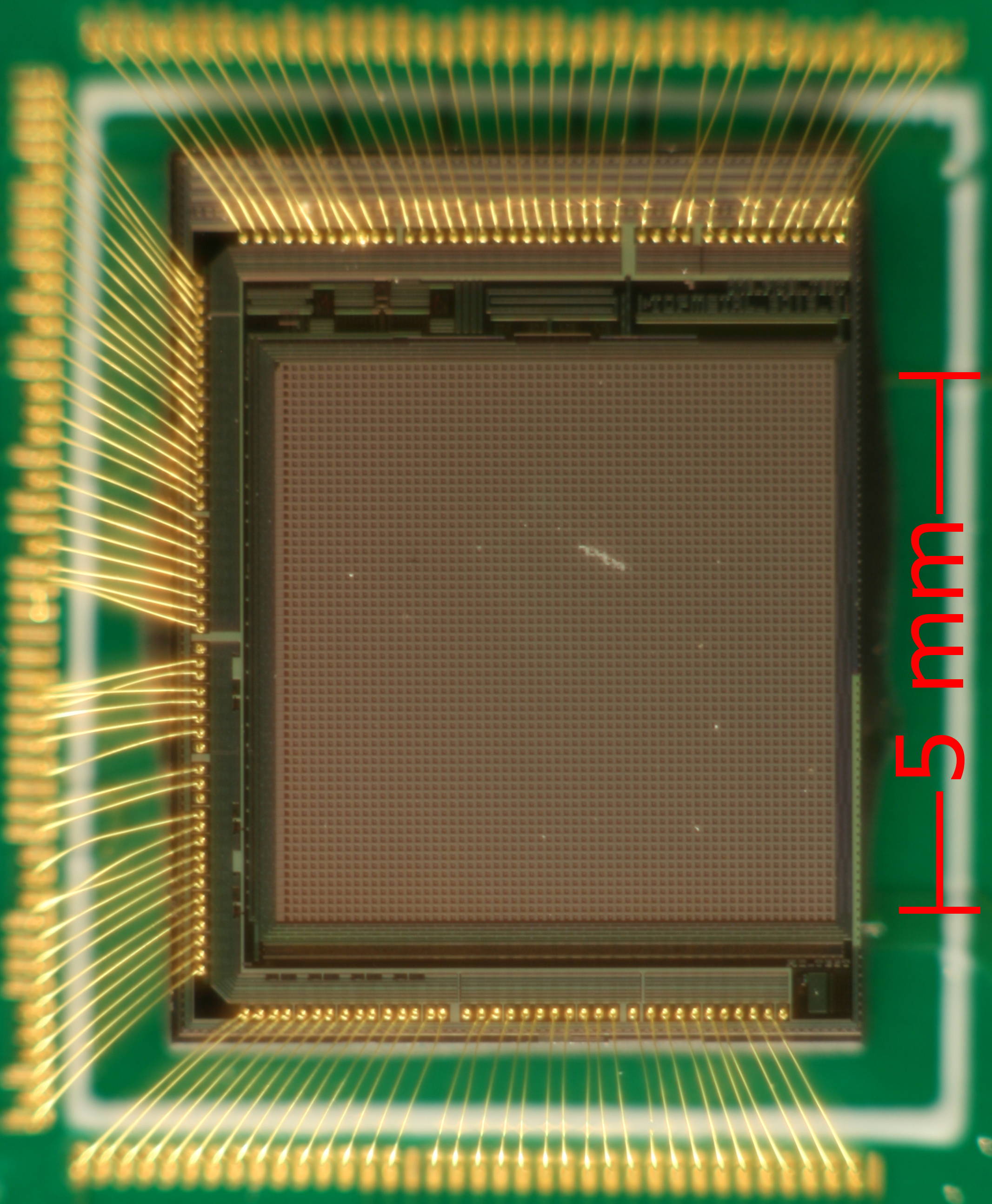

The pixel array is divided into sub-arrays for efficient analog readout. As shown in Fig. 1, each sub-array is of rows by columns in size and has one dedicated analog output buffer per sub-array. A single external clock drives the analog row/column multiplexing readout circuitry in each of the sub-arrays synchronously.
The internal structure of a single pixel is illustrated in Fig. 2. The Topmetal is implemented with the PROBEPAD component in the standard CMOS process, which is a patch of metal in the topmost layer and has a part of it not covered by the passivation layer. We designed the metal patch to be in size, with the central exposed hence sensitive to external charge. The metal patch is large enough to be mechanically and chemically stable, while small enough to suppress the cross-talk between neighboring pixels to a negligible level.
Charges arrived at the sensor and collected by the Topmetal result in an electric potential change at the “Node”, which is a detectable signal. The potential of the “Node”, , is captured by means of a source follower that drives the signal through row/column multiplexer for analog readout. The equivalent capacitance of Topmetal to ground is measured to be approximately . It means electrons collected by Topmetal would correspond to voltage drop on the “Node”.
The resetting circuit for the “Node” allows controlled removal of charge collected by the Topmetal and the initial potential setting of the node. When a logic high is applied to the reset gate, the “Node” potential is set to and any excess charge on the “Node” is neutralized by the power supply driving .
Two test columns are implemented in the leftmost sub-array (Fig. 1). Pixels in the first test column have identical structure as the rest of the pixels, except that the “Node” is internally connected to ground. They serve as markers in the multiplexed readout. Since their is fixed internally, they are immune to the noise generated by the Topmetal capacitance. Noise measurements on the first test column measures the noise due to the analog readout path only, decoupled from that from the Topmetal. Pixels in the second test column have the “Node” capacitively coupled to an external pin. They were designed to test the pixel response to pulses injected from the external pin. The pin is tied to ground during normal operations.

Charge signal in each pixel is also converted into digital values by means of a threshold discriminator (comparator), a delayed resetter, and a 5-bit counter. Muxing readout for digital data at array level is also implemented. The digital data chain is suitable for charge event counting applications. However, in this letter, we focus on the physical behavior and analog characteristics of the device.
3 Signal Formation
The Topmetal can be modeled as a resistor with large resistance and a capacitor with small capacitance connected in parallel (Fig. 2). The time constant is on the order of . During charge collection, the equivalent charge current will run through the resistor while charging up the capacitor at the same time. The following differential equation gives the general behavior of the circuitry:
| (1) |
is the voltage across the capacitor, which is then measured.
The solution to the differential equation is
| (2) |
The time-dependent solution is the most generic. The solutions for and are two special cases. The boundary conditions are set such that no matter whether there is a charge current or not, at , the output voltage is set to a defined reset value . When collecting electrons (negative charge), , otherwise .
The sudden arrival of a charge pulse can be modeled as , where is the arrival time of the charge pulse. At , the voltage decay curve drops by the amount of , as shown in Fig. 3.
Ideally, we can build an algorithm to find the sudden drops and reconstruct their amplitudes to measure the charge collected. However, due to the noise, as seen in Fig. 3, such an approach is unlikely to be robust. Also, in the case of continuous charge current, there will be no sudden drop. Instead, to extract the charge information, we employ a “double subtraction” scheme.
Prior to the charge measurement, we remove the charge source, but operate the sensor in the same condition, to establish a baseline. The baseline, , is a time-series measurement of node voltage without charge input. During the charge measurement, we record in a similar fashion. The baseline and charge measurements are synchronized by a periodical reset signal. The time between two resets defines an event window, and is the charge integration time. We subtract the voltage right after reset, , from the voltage at the end of the window, , in each case, then subtract the difference in baseline from that in charge measurement. The quantity is shown in Eq. (3).
| (3) | ||||
In the limit where ,
| (4) |
hence
| (5) |
Eqs. (3–5) are derived assuming a constant current . It can be shown that the same relation Eq. (5) holds for sudden charge arrivals.
We operate at a charge integration time window of tens of milliseconds, so that Eq. (4) is satisfied. Therefore we can use the simple proportional relation Eq. (5) to compute the charge value. We also refer to one measurement an “event”.

The node voltage behavior in a characteristic pixel is shown in Fig. 3. When the reset is activated (), the node is set to the voltage of . As soon as the reset is deactivated, due to charge injection on the MOS transistor [10], the node voltage drops to a deterministic value. In this example, the node voltage right after reset is about . Up to a small fluctuation, the baseline curve behaves identically after each reset for the same pixel. Then, when there is no charge being collected, the node voltage changes exponentially towards a stable value. When the charges arrive, the voltage curve shows a sudden drop.
Due to the inhomogeneity of the CMOS process, the baseline curves behave differently among pixels. The most significant variation is in the decay time constant. Nevertheless, it is only necessary to calibrate the baseline curves for every pixel once prior to the charge detection.
To image 2D distributions of the charge cloud, the above procedure is performed on each pixel in the array. The temporal behavior of each pixel is decoded from the multiplexed readout signal. The interval of sampling is the pixel clock period times the number of pixels in a sub-array (1024). The time between resets is set to be slightly larger than the desired charge integration time. is then computed for each pixel and the 2D distribution is established.
4 Charge Calibration
To demonstrate that the Topmetal-I sensor is capable of directly detecting charge, and to calibrate for charge measurements, we constructed a rudimentary drift chamber, using an alpha source to ionize air, then drift the negative charge towards the sensor in an electric field.
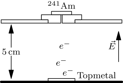
We wire-bonded a Topmetal-I sensor onto a PCB and placed supporting circuity on the PCB to drive the sensor and to transmit analog signals out via coax cables. On the other end of the coax cables, signals are digitized by a 14-bit high speed ADC. To create a uniform drift field with field lines perpendicular to the sensor, we placed a large aluminum plate above, and parallel to the sensor, serving as the cathode. While the sensor substrate and the PCB are placed close to ground potential, the aluminum plate is held at , creating an electric field of .
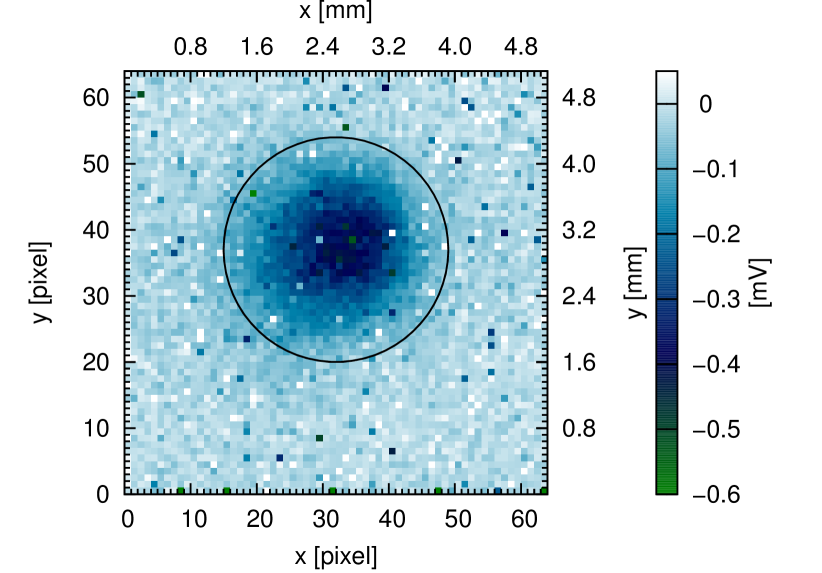
A collimated source embedded in the cathode emits alpha particles perpendicular to the sensor. The alphas ionize air along their paths. Negative charge generated during the process is drifted towards the sensor and eventually collected by the sensor. Alphas from the source have a range of about in air at standard temperature and pressure [11]. The distance between the cathode and the sensor () was chosen so that alphas would deposit their full energy in air instead of hitting the sensor. An averaged image of the charge cloud from alphas seen by the sensor is shown in Fig. 5.
The event time window is and the integration time is . Effectively we are collecting data at an event rate of . The collimator limits the alpha rate to be much lower than the data event rate. The conditions are chosen so that within a data event, there can be either zero or one alpha, and the probability of two or more alphas in the same event becomes negligible. Meanwhile, the integration time is long enough to fully collect the charge after an alpha interaction, since it takes only microseconds for electrons to drift for [12].

On average, each alpha particle emitted from the source deposits [13] energy in air resulting in ionization. The air has an ionization -value of [14]. Since alphas are fully stopped before hitting the sensor, and electrons are fully collected during the integration time, each alpha event results in a mean value of approximately . Since each event has either zero or one alpha, if we plot a histogram of the voltage signal due to charge, we should be able to identify a peak corresponding to single alphas, and use the relation
| (6) |
to compute the capacitance of a single pixel. is the total charge and the summation is over pixels that see charge.
’s of pixels within a radius (Fig. 5) are summed up to fill the histogram in Fig. 6. The region is chosen such that of charge is contained in the region given the signal is modeled by a two-dimensional Gaussian distribution. We will not attempt to correct for the potential loss of charge, instead, we treat it as a systematic uncertainty of the measurement. The single-alpha peak is clear in Fig. 6 and is well characterized by a Gaussian function. From the mean voltage value of the single-alpha peak, we measure the pixel capacitance . The uncertainty, a combination of uncertainty from the fit and the systematic uncertainty, is found to be .
To validate the result, we used a less stringent collimator to increase the total ionization per unit time. Under the same electric field, we measured the ionization current with a picoammeter to be around . The ionization current is then collected by the Topmetal-I sensor operating under exactly the same condition. The measurement yields a similar capacitance value, with larger uncertainty.
To evaluate the noise performance of the sensor, we use the baseline dataset alone, and compute the Root-Mean-Square (RMS) of voltage drop of each pixel across all events. The noise is then calculated as , where is the above measured pixel capacitance. The RMS voltage drop distribution of the entire pixel array is shown in Fig. 7. The distribution has three distinct clusters. The cluster with the lowest RMS value contains the test pixels in the first column. Those pixels have their voltages tied to a fixed value at all times. The RMS value of them comes solely from the analog readout noise. It provides a measurement of the analog readout noise independent of the noise from the Topmetal capacitance. The second test column is capacitively coupled to an external pin therefore has higher noise. The RMS of the main array has its most probable value at , which corresponds to about . The uncertainty of this value is solely determined by the uncertainty of capacitance measurement.

During normal air-cooled operations, the sensor temperature stabilizes at about . A capacitor at such temperature has an intrinsic thermal noise of [15]. Using the first test pixel column, we determine that the analog readout system has an ENC of . The quadratic summation of the two noise values yields , which is very close to the most probable ENC value of the main pixel array. It indicates that the equivalent capacitor of the Topmetal is operating near its thermal noise limit.
5 Summary
We have demonstrated the possibility of implementing a highly pixelated sensor for direct charge collection using industrial standard CMOS technology. No post-processing is necessary. Although in this first attempt, Topmetal-I, the sensor noise is moderately high, its capability in observing charge from single-alpha events in air directly already shows its potential in applications.
The design and production of CMOS IC are traditionally perceived as inhibitively expensive. However, recent advancement in the industry has made the mature technologies such as the process affordable. Also, the direct charge collection capability, without the need of any post-processing, makes the overall integration cost much lower than for example technologies used in producing hybrid solid-state detectors.
To improve beyond Topmetal-I, besides reducing the pixel size, we can further reduce the noise and record the charge arrival time. By placing a charge sensitive amplifier in each pixel, and reducing the Topmetal size hence its capacitance, we foresee an ENC better than per pixel should be achievable. Information on charge arrival time can be obtained using an individually addressable pixel structure. We will explore these options in future series of Topmetal sensors.
Acknowledgments
This work is supported, in part, by the Thousand Talents Program at Central China Normal University and by the National Natural Science Foundation of China under Grant No. 11375073. We also acknowledge the support from LBNL for hosting the physical measurements of the sensor. We would like to thank Christine Hu-Guo and Nu Xu for fruitful discussions.
References
- Ballabriga et al. [2011] R. Ballabriga, M. Campbell, E. Heijne, X. Llopart, L. Tlustos, W. Wong, Medipix3: A 64k pixel detector readout chip working in single photon counting mode with improved spectrometric performance, Nuclear Instruments and Methods in Physics Research Section A: Accelerators, Spectrometers, Detectors and Associated Equipment 633, Supplement 1 (0) (2011) S15 – S18, ISSN 0168-9002, URL http://www.sciencedirect.com/science/article/pii/S0168900210012982.
- Llopart et al. [2007] X. Llopart, R. Ballabriga, M. Campbell, L. Tlustos, W. Wong, Timepix, a 65k programmable pixel readout chip for arrival time, energy and/or photon counting measurements, Nuclear Instruments and Methods in Physics Research Section A: Accelerators, Spectrometers, Detectors and Associated Equipment 581 (1–2) (2007) 485 – 494, ISSN 0168-9002, URL http://www.sciencedirect.com/science/article/pii/S0168900207017020.
- Garcia-Sciveres et al. [2010] M. Garcia-Sciveres, et al., The FE-I4 pixel readout integrated circuit, Nucl. Instr. and Meth. A 636 (2010) S155–S159.
- Marx and Nygren [1978] J. Marx, D. Nygren, The Time Projection Chamber, Phys. Today 31 (10) (1978) 46.
- Aprile et al. [1996] E. Aprile, V. Egorov, F. Xu, E. L. Chupp, P. P. Dunphy, T. Doke, J. Kikuchi, G. J. Fishman, G. N. Pendleton, K. Masuda, T. Kashiwagi, Liquid Xenon Gamma-Ray Imaging Telescope (LXeGRIT) for medium energy astrophysics, URL http://dx.doi.org/10.1117/12.253996, 1996.
- Nagayoshi et al. [2004] T. Nagayoshi, H. Kubo, K. Miuchi, R. Orito, A. Takada, A. Takeda, T. Tanimori, M. Ueno, O. Bouianov, M. Bouianov, Development of -PIC and its imaging properties, Nuclear Instruments and Methods in Physics Research Section A: Accelerators, Spectrometers, Detectors and Associated Equipment 525 (1–2) (2004) 20–27, ISSN 0168-9002, URL http://www.sciencedirect.com/science/article/pii/S0168900204003419.
- Vahsen et al. [2012] S. E. Vahsen, H. Feng, M. Garcia-Sciveres, I. Jaegle, J. Kadyk, Y. Nguyen, M. Rosen, S. Ross, T. Thorpe, J. Yamaoka, The Directional Dark Matter Detector (D3), EAS Publications Series 53 (2012) 43–50.
- Aad et al. [2008] G. Aad, et al., The ATLAS Experiment at the CERN Large Hadron Collider, JINST 3 (2008) S08003.
- Brezina et al. [2012] C. Brezina, K. Desch, J. Kaminski, M. Killenberg, T. Krautscheid, Operation of a GEM-TPC With Pixel Readout, IEEE Transactions on Nuclear Science 59 (6) (2012) 3221.
- Shieh et al. [1987] J.-H. Shieh, M. Patil, B. J. Sheu, Measurement and Analysis of Charge Injection in MOS Analog Switches, IEEE Journal of Solid-State Circuits SC-22 (2) (1987) 277.
- Berger et al. [????] M. J. Berger, J. S. Coursey, M. A. Zucker, Stopping-power and range tables for electrons, protons, and helium ions, National Institute of Standards and Technology URL http://physics.nist.gov/PhysRefData/Star/Text/ASTAR.html.
- Hegerberg and Reid [1980] R. Hegerberg, I. D. Reid, Electron drift velocities in air, Aust. J. Phys. (1980) 227–230.
- Basunia [2006] M. S. Basunia, Nuclear Data Sheets 107 (2006) 3323.
- Giesen and Beck [2013] U. Giesen, J. Beck, New Measurements of W-Values for Protons and Alpha Particles, Radiation Protection Dosimetry (2013) 1–4.
- Sarpeshkar et al. [1993] R. Sarpeshkar, T. Delbruck, C. A. Mead, White noise in MOS transistors and resistors, IEEE Circuits Devices Mag. (1993) 23–29.